1. Introduction
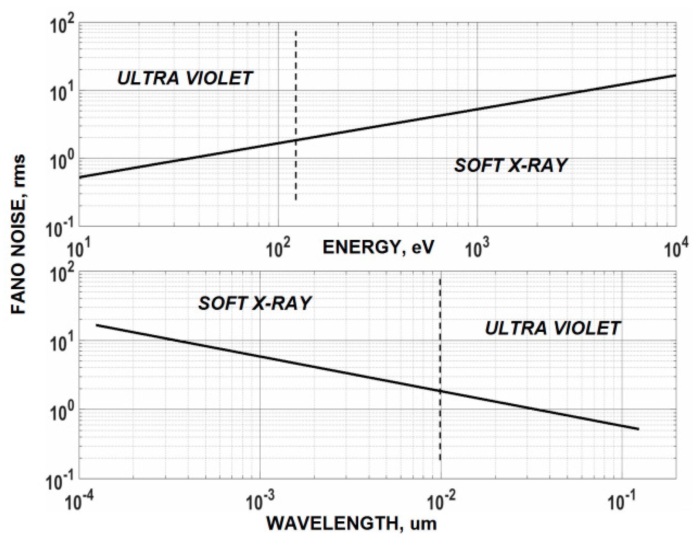
Silicon CCD and CMOS imagers have been demonstrated to be exceptional detectors for particle counting and energy measurement for some time. The spectral range where photon counting is possible covers an extensive wavelength range from 0.1 to 1000 nm (1.24 to 12,400 eV),
i.e., nIR, visible, UV, EUV and soft X-ray. At the beginning of the EUV range (10 eV) photon energy absorbed by the imager can be determined by using the simple relation [
1],
where 3.65 is an experimentally determined constant for silicon (eV/carriers) and
ni is measured quantum yield (carriers generated/interacting photon). The equation is applicable to photon energies greater than ~10 eV. The formula is not useful for energies less than this because the constant 3.65 wildly fluctuates. Besides photons, this equation is also useful for any particle that ionizes silicon atoms (electrons, protons, muons,
etc.). The uncertainty in energy measurement is limited by the detector’s read floor and Fano noise. Fano noise, the variation of charge generated per photon, is found by,
where
F is the Fano factor (~0.1 for silicon) and
ni is the quantum yield (carriers generated per photon). Physically Fano noise arises within the silicon where a small amount of thermal energy is lost to the silicon lattice (phonons) instead of creating electron-hole pairs. The variation in the loss from pixel to pixel is the Fano noise generated and represents a fundamental noise source in determining the energy of high energy particles [
2].
Imagers where Fano noise is greater than the sensor’s read noise are referred to as “Fano noise limited” [
2].
Figure 1 plots Fano noise as a function of photon energy (eV) and wavelength (µm) showing the Fano limited range that can be covered by an imager for a given read noise floor. For example,
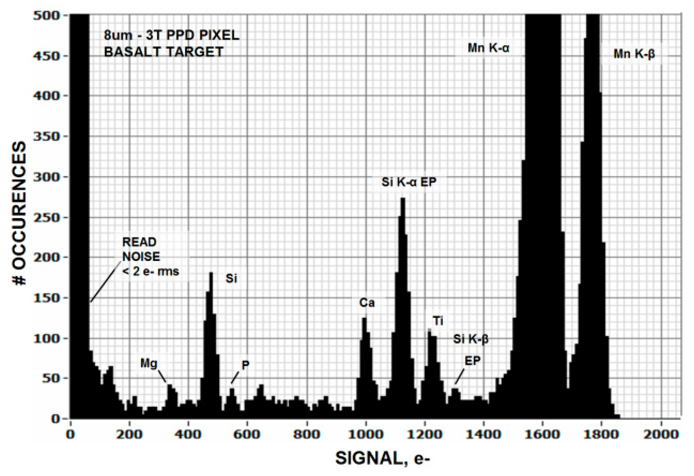
Figure 2 presents a histogram taken from a Fano noise limited 8 um 3T NMOS pinned photo diode (PPD) pixel array showing multiple energy lines from a basalt target fluoresced with 5.9 keV Mn X-rays. The sensor’s read noise is slightly less than 2 electrons (e
−) allowing Fano limited performance to cover the entire soft X-ray range (0.12 nm–10 nm). This spectral range has been particularly fruitful for CCD soft X-ray imaging spectrometers used in scientific and space applications. The width of each spectral line revealed in
Figure 2 is a measurement of the amount of Fano noise generated. The spectral range for this imager can be further extended into the EUV range (10 nm–124 nm) if only photon counting is desirable.
The photon energy for visible (400 nm–700 nm) and nIR (700 nm–1100 nm) wavelengths is only able to generate one electron-hole pair/photon, limiting sensing to only photon counting. But when leaving the visible range into the UV multiple carriers per photon are generated allowing their energy to be determined. The challenge left today is to extend energy measurement into the UV and provide photon counting in the visible/nIR wavelengths by reducing the sensor’s read noise floor.
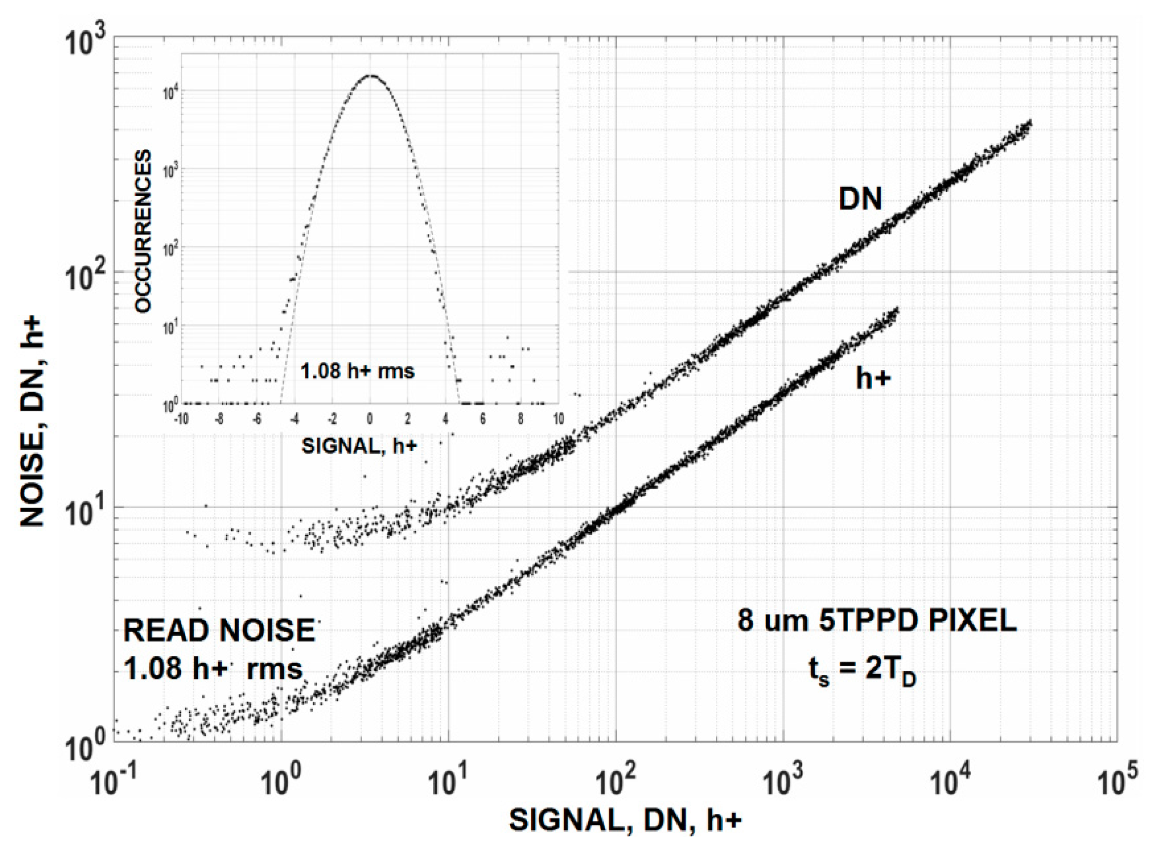
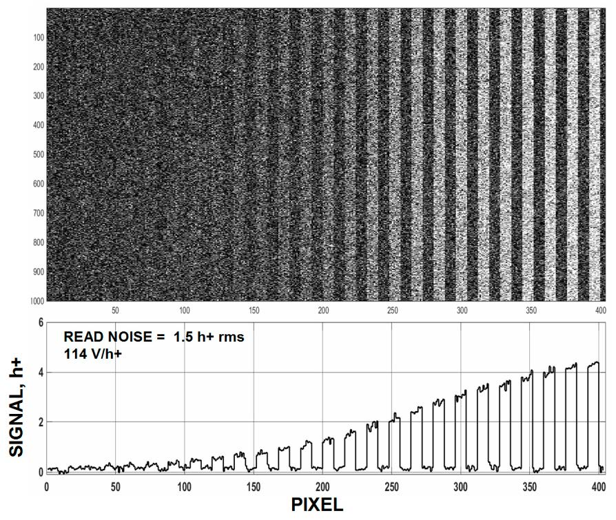
The average noise floor for high performance CCD and CMOS imagers is typically shy of achieving “one” carrier of noise (this excludes EMCCD and SPAD detectors). For example,
Figure 3 presents a photon transfer (PT) [
2,
3] curve generated by a 512 um × 512 um × 8 um PPD PMOS CMOS imager with a read noise floor of 1.08 holes (h+ )at room temperature. It is extraordinary that the CCD/CMOS imaging community for the most part has achieved approximately “one” carrier of noise considering the multitude of solid state phenomena at play at world wide fabrication foundries for several years (decades in the case of CCDs). But why “one”? Is this apparent final outcome simply coincidental? One also wonders further why “one” carrier of noise along with “one” carrier of signal forces the minimum detection limit (MDL) of the detector to be “one” (
i.e., S/N = “one”). The conundrum continues with why today’s imagers are very close but yet so far from “routinely” counting single visible photons consistently across full imaging arrays.
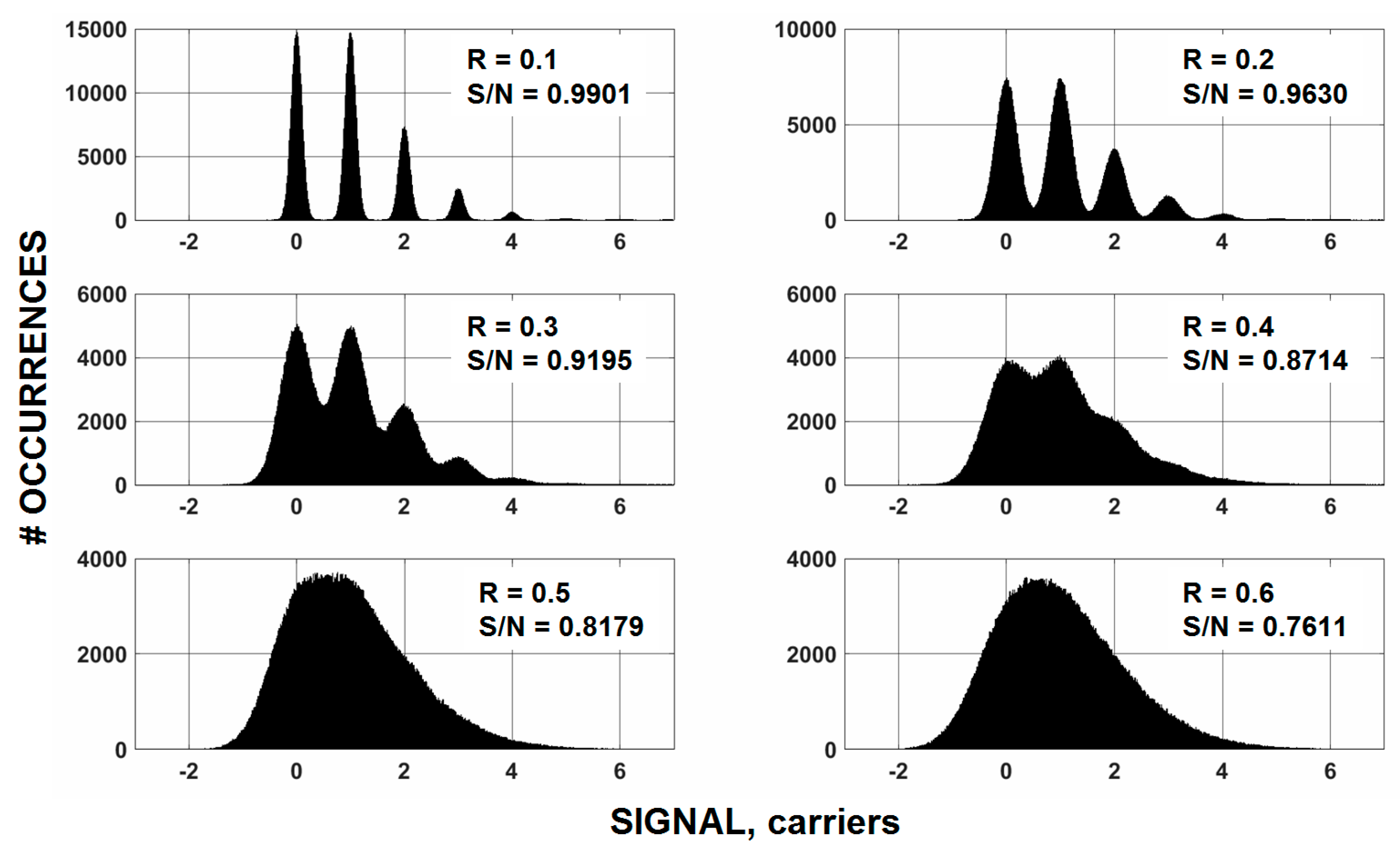
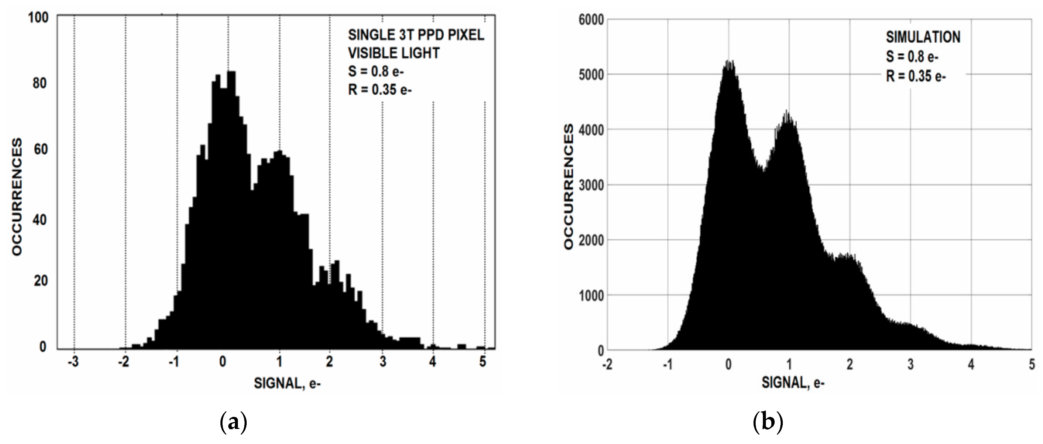
To appreciate the challenge,
Figure 4 displays computer simulated histograms for different read noise levels for an average signal level of “one” interacting photon/pixel and quantum yield of “one”. These plots show that it is necessary to have a read noise floor of <0.3 e
− before the histograms appear “quantized”, which in turn sets the stage for visible/nIR photon counting. Also notice from these plots that the net signal-to-noise (S/N) determined directly from the simulated plots hardly changes as read noise is lowered from 0.3 to 0.1 carriers because the presence of photon shot noise. Nonetheless, read noise improvement in this range is especially critical to future visible/nIR photon counting imagers and applications.
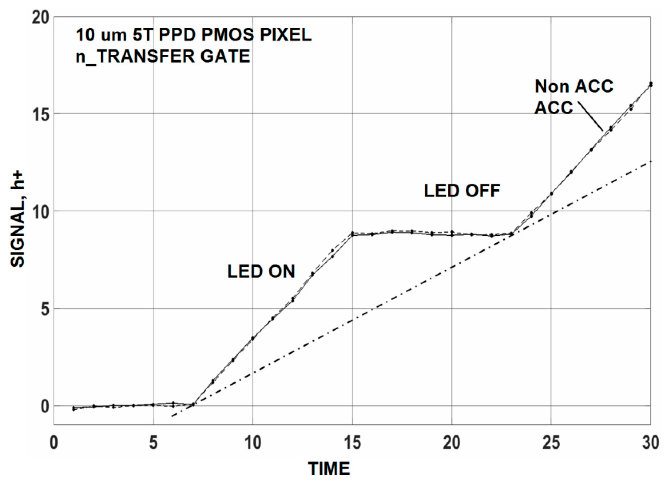
Occasionally we do run into an individual low noise pixel that is capable (but barely) of photon counting allowing us to see the Poisson distribution profile that governs photon counting statistics. The top histogram of
Figure 5a is generated by an exceptionally low noise “cherry picked” NMOS 3T PPD pixel with a 0.35 e
− noise floor taken under cooled conditions (~−80 °C). An average signal level of 0.8 e
− is adjusted for the experiment (
i.e., 0.8 interacting photons/pixel). The lower histogram shown in
Figure 5b is a computer simulation showing that data and theory match up quite well.
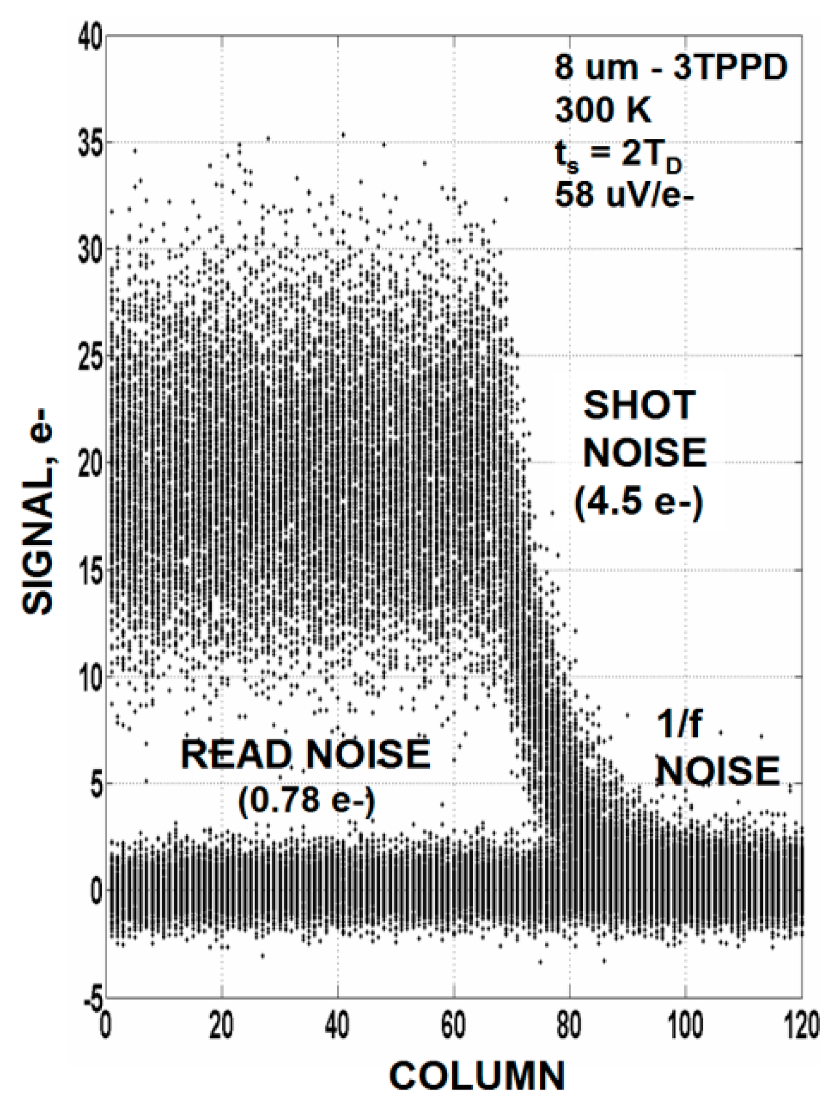
Figure 6 is a different NMOS 3T pixel illustrating how 4.5 e
− photon shot noise folds into the 0.78 e
− noise floor as the light source slowly turns off. These low noise pixels imply that the “one” carrier noise level that manufacturers have produced may not represent a fundamental limit but simply related to the noise level being “good enough”. This stance is reasonable to assume because for normal imagery the S/N is always less than “one” regardless of how much lower the read noise is beyond “one”. Hence, imager manufactures may not feel obligated to aggressively lower read noise any further (especially monetarily). This position produces an illusion that there may be a physical barrier of some kind holding us to “one” noise carrier. Fairly recently (2015) it has become more apparent that the “one” noise barrier has been a deception for groups are now reporting sub carrier performance down to 0.23 e
− for selected pixels [
4,
5] allowing for visible photon counting. The future objective for sensors with sub carrier read noise floors is to have all pixels contained on an imager exhibit close to the same low noise level and not just a few while at the same time achieve a reasonable saturation level for high dynamic range.
2. Read Noise Reduction
2.1. Flicker and Random Telegraph Noise
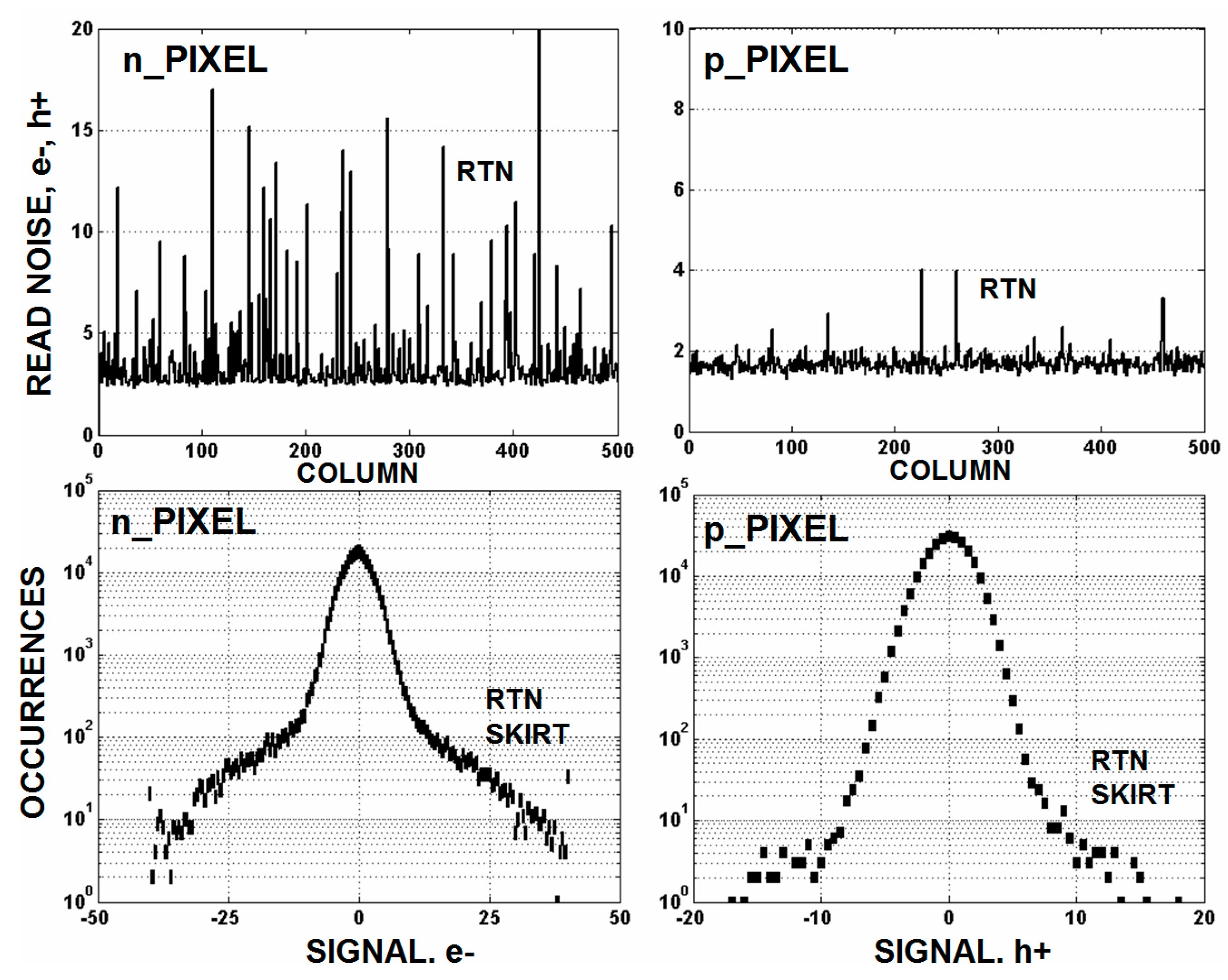
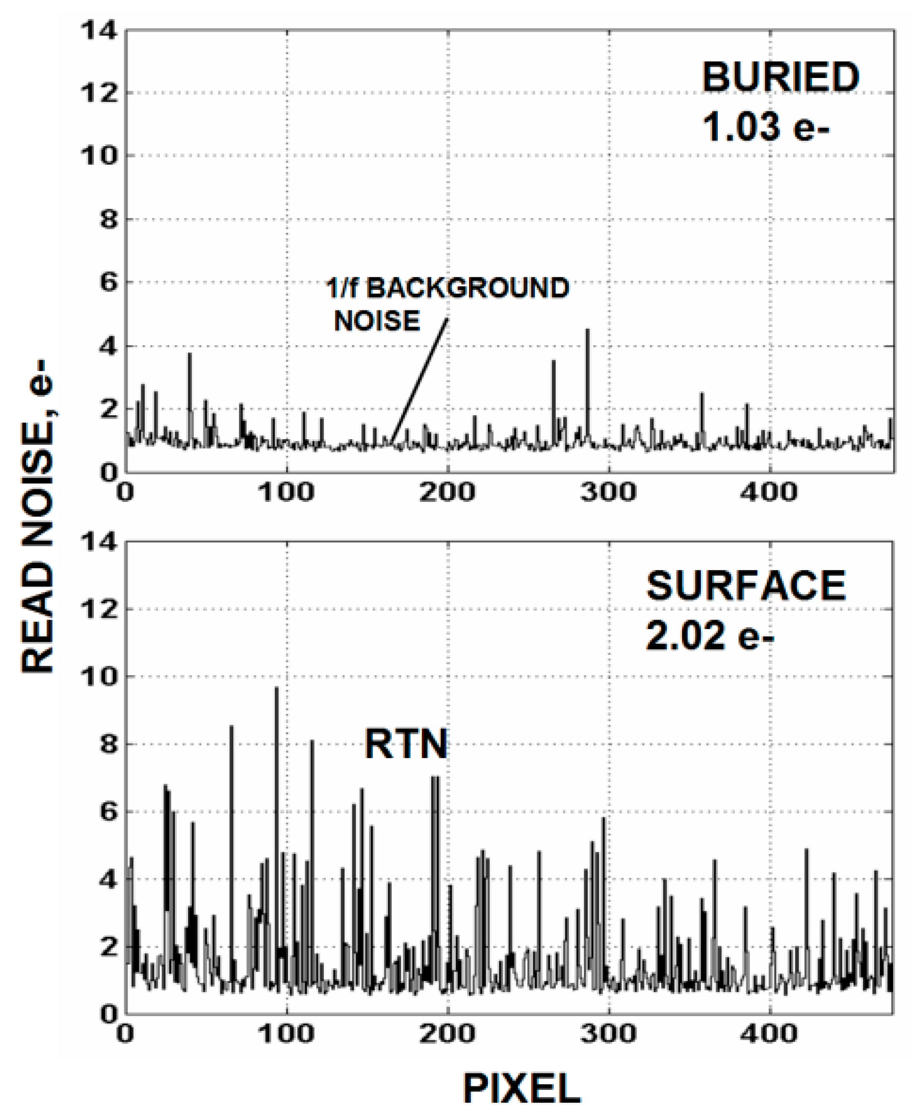
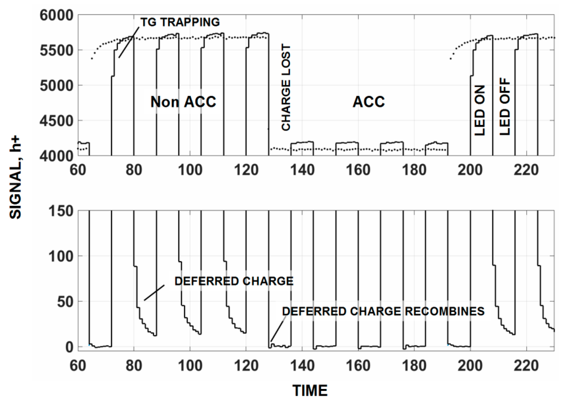
Flicker and random telegraph noise (RTN) generated by the pixel’s source follower (SF) MOSFET are the dominant noise sources that limit read noise performance for an imager. It is generally believed that RTN is associated with traps within the gate oxide. Free carriers from the SF channel tunnel in and out of these traps at different rates depending on the tunneling distance to the trap and the barrier height encountered. The local “on” and “off” potential in the localized region of a trapped carrier modulates the SF channel current in a digital manner and is seen as RTN output voltage fluctuation (with varying amplitude and frequency from pixel to pixel depending on the trap time constant and location). NMOS imagers have a great deal more RTN pixels than PMOS devices do. For instance,
Figure 7 compares the read noise for NMOS and PMOS pixels showing very few RTN pixels for the PMOS imager. The background flicker noise levels are different for the plots because the sense node (SN) conversion gains are not the same. However, it is observed that when the sensitivity is the same the background flicker noise level (rms carriers) is nearly identical for PMOS and NMOS pixels.
Other sources of pixel noise have been observed that mimic SF RTN. For example, a poor SN metal contact exhibits RTN behavior. Leakage currents related to the pixels transfer gate (TG) and reset gate that are in close proximity to the SN can also contribute noise for some local pixels. However, one can usually differentiate these noise sources from SF noise by varying the voltages to these gates and the SN reset bias level and noting the affect.
The reason for the NMOS/PMOS RTN population difference is holes are much less likely to tunnel into oxide traps than electrons because the barrier height is greater. On these grounds we do not need to consider RTN as a fundamental barrier to lowering read noise. Therefore, the problem of beating down SF flicker noise has become the only fundamental noise source in reducing the read noise floor for PMOS imagers. However, for NMOS devices we must use other strategies to reduce RTN. For example buried channel MOSFETs can be employed which to some degree isolates the SF current carrying channel from the surface. In turn this increases the barrier to the traps and lowers RTN. We will briefly discuss this technology below.
Two primary theories describe flicker noise generation in MOSFETs: Hooge’s mobility fluctuation and McWhorter’s carrier density (or number) fluctuation models [
6,
7]. The latter mechanism is based on the random trapping and release of conduction band carriers located at the Si-SiO
2 interface of the SF MOSFET (
i.e., generation recombination (GR) noise). The former is related to conductance or resistance fluctuations within the channel of the SF MOSFET. There are several possible causes for channel mobility noise. For example, fluctuations may be associated with a lower surface mobility compared to bulk silicon because carriers scatter off the Si-SiO
2 interface. Another possibility could be linked to the SF channel’s implanted impurities that are randomly imbedded in the silicon lattice. The depleted ions in the SF channel produce small individual potential barriers that “fluctuate” current flow thus producing noise [
8].
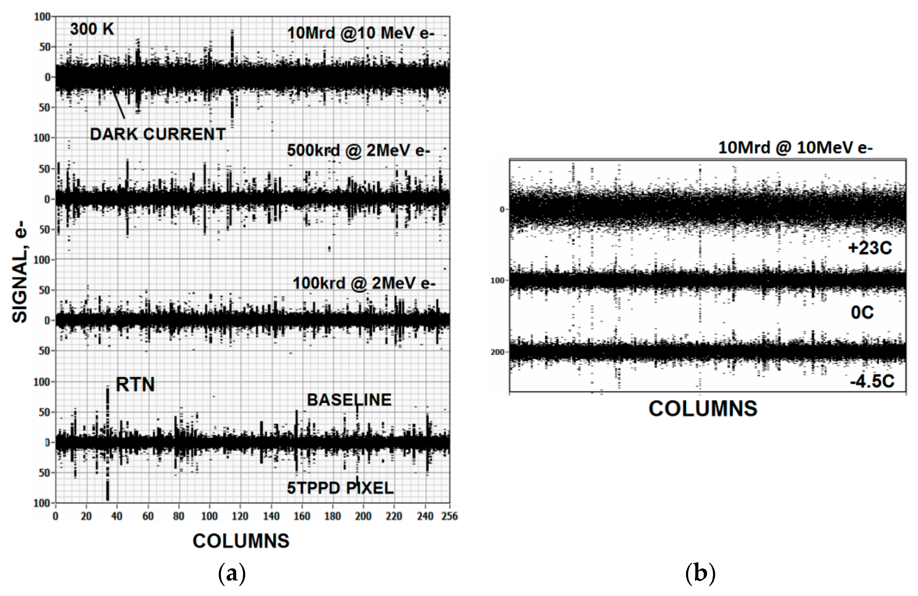
To help identify where 1/
f noise sources are located, pixels have been irradiated with high energy radiation sources to deliberately increase interfacial Si-SiO
2 surface states. In general when such experiments are performed we find that the read noise level does not change. For example,
Figure 8a shows that the read noise remains constant after irradiating an unbiased NMOS CMOS imager to different dose levels of high energy electrons. The noise data shown was generated using a very short exposure time (~10 µs) such that the increase in dark current shot noise due to radiation damage was negligible. However, the read noise for 10 Mrd exposure appears to be higher because thermally generated dark current was high enough to become an issue. Cooling the pixels slightly as displayed in
Figure 8b lowers the noise down to the same level as other irradiated imagers.
The same sensors irradiated did exhibit charge transfer efficiency (CTE) degradation related to the TG demonstrating that surface states were in fact being generated. Some flat-band shift due to positive fixed charge buildup in the oxide induced by the radiation was also measured again indicating some damage took place but without a read noise increase. Other research groups have experienced the same surprising outcome [
6]. Although far from being proven these findings begin to bias us to believe that the background flicker noise may not be dominantly associated with the oxide but instead within the current carrying channel of the SF.
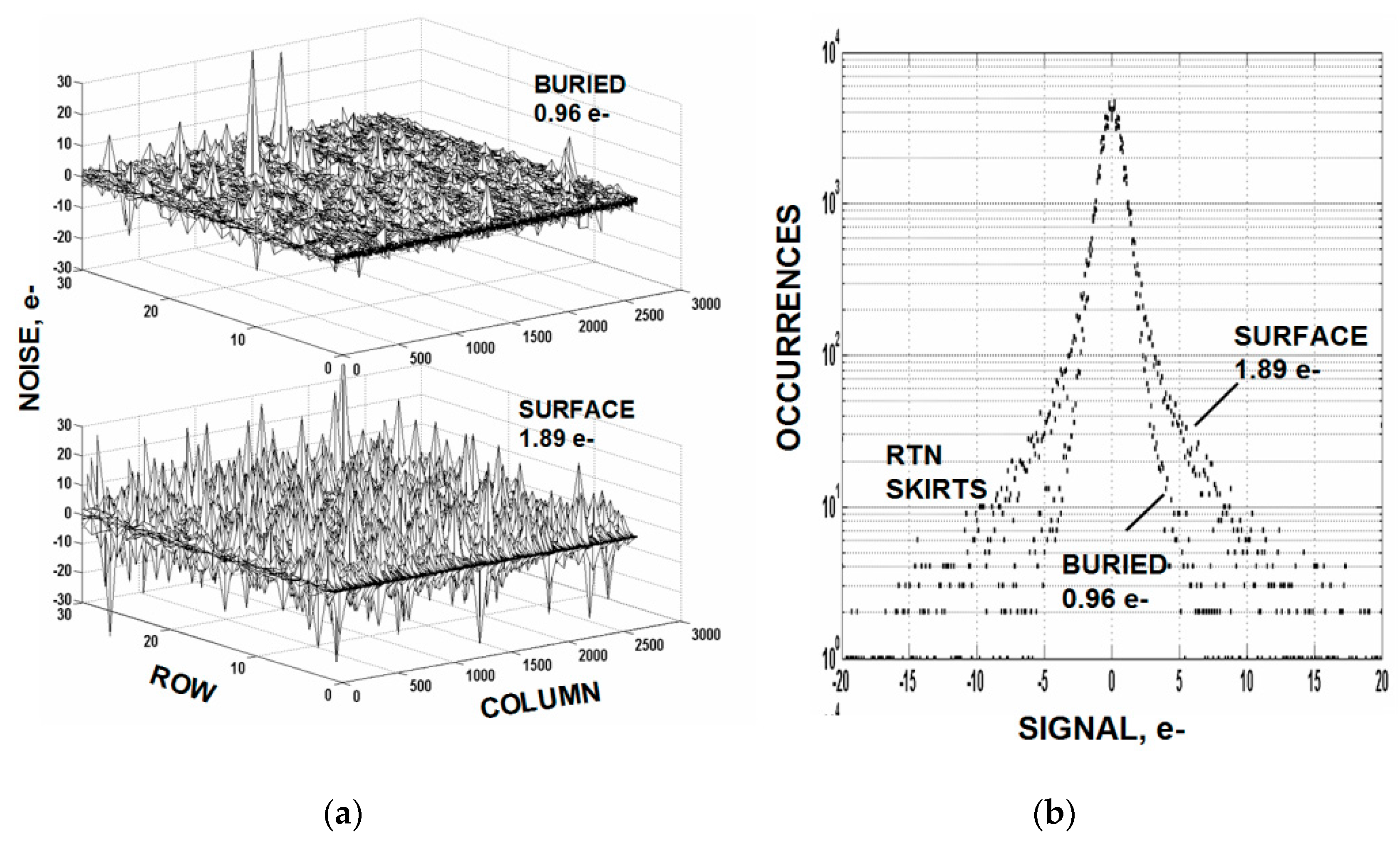
We have had some past success in reducing read noise using buried channel NMOS MOSFETs. Others working with this approach have realized the same benefit [
9]. For example,
Figure 9a,b shows the temporal noise difference for surface and buried channel MOSFETs. Notice that a significant RTN noise reduction takes place with buried use but does not change the background 1/
f noise.
Figure 10 also shows an unchanged background noise level for a row of 500 pixels where the rms noise level is determined for each pixel. The outcome is reasonable for RTN because the barrier increase provided by buried channel should diminish electron tunneling into the oxide. But why not a 1/
f noise reduction? Possibly the buried channel employed here did not provide a sufficient barrier or shield deep enough for bulk generated 1/
f noise. Or perhaps the 1/
f noise is being generated in another location or mechanism other than just traps.
2.2. Correlated Double Sampling
Flicker noise and correlated double sampling (CDS) share a fascinating relationship. Analysis and measurements show that optimum flicker noise reduction takes place when:
where t
s is the time difference between samples before and after charge is transferred to the SN and B is the net equivalent noise bandwidth for the sensor and CDS system [
10]. Equation (3) can also be expressed as t
s = 2τ
D where τ
D is the system dominate time constant.
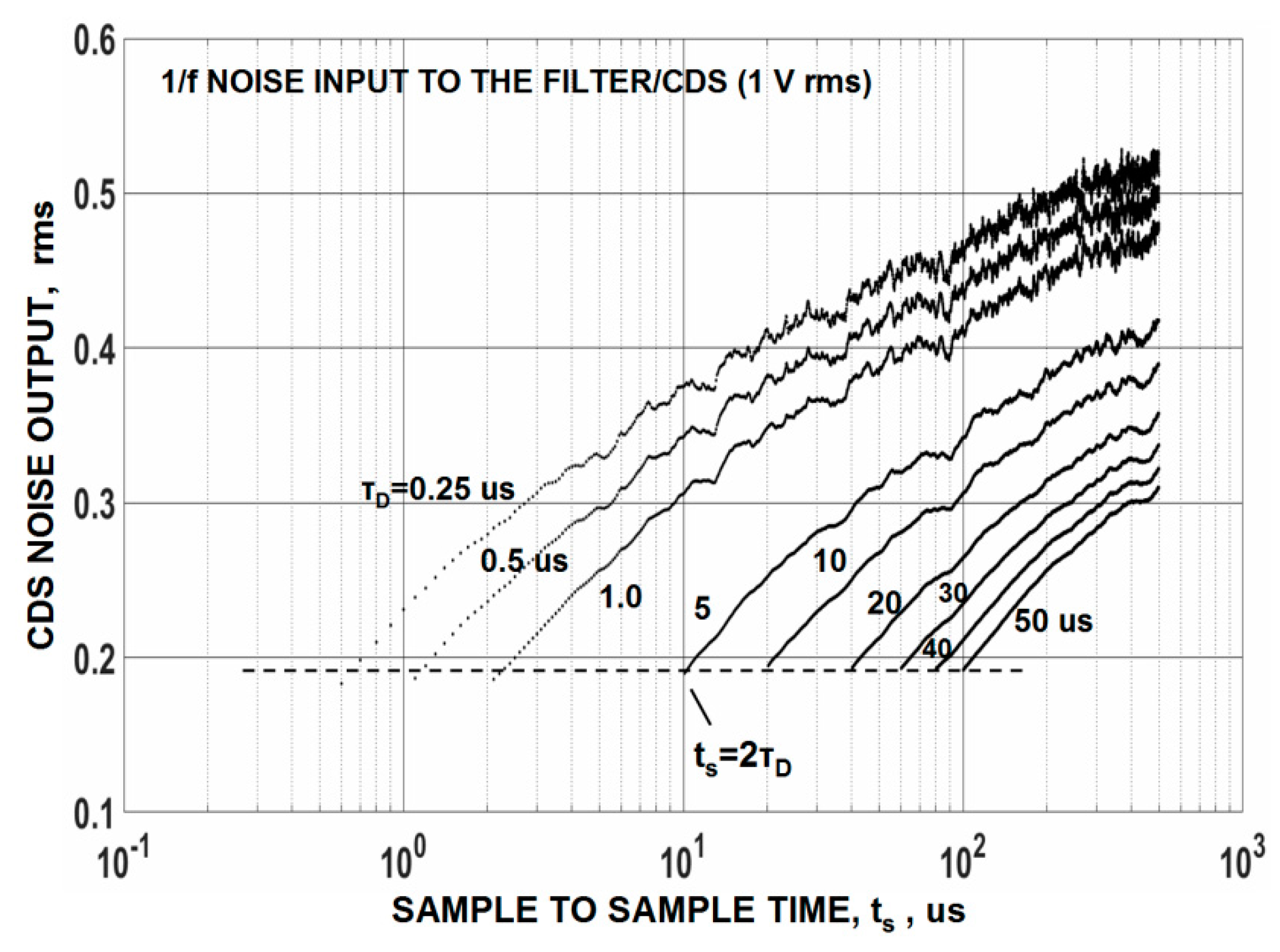
Figure 11 plots CDS output noise as a function of t
s for various τ
D for a flicker noise input. For a specified τ
D the output noise increases with t
s because 1/
f noise correlation is being lost between the two samples. For very long t
s time the CDS output noise will eventually level off to 2
0.5 times the input noise because the samples are fully uncorrelated and differenced. It is important to point out from this plot that CDS output noise is constant with t
s given that t
s = 2τ
D is fixed (
i.e., the dotted horizontal line shown on the plot). Under this timing boundary condition 1/
f noise decreases with τ
D at the same rate as 1/
f noise increases with t
s. This is the central reason why it’s not feasible to eliminate 1/
f noise by CDS processing. It should be mentioned that sampling less than 2τ
D results in a signal gain loss and lower S/N performance (the reason why the plots are bounded by the dotted horizontal line). Also, sampling an exponentially changing video waveform can produce camera instabilities (e.g., offset control).
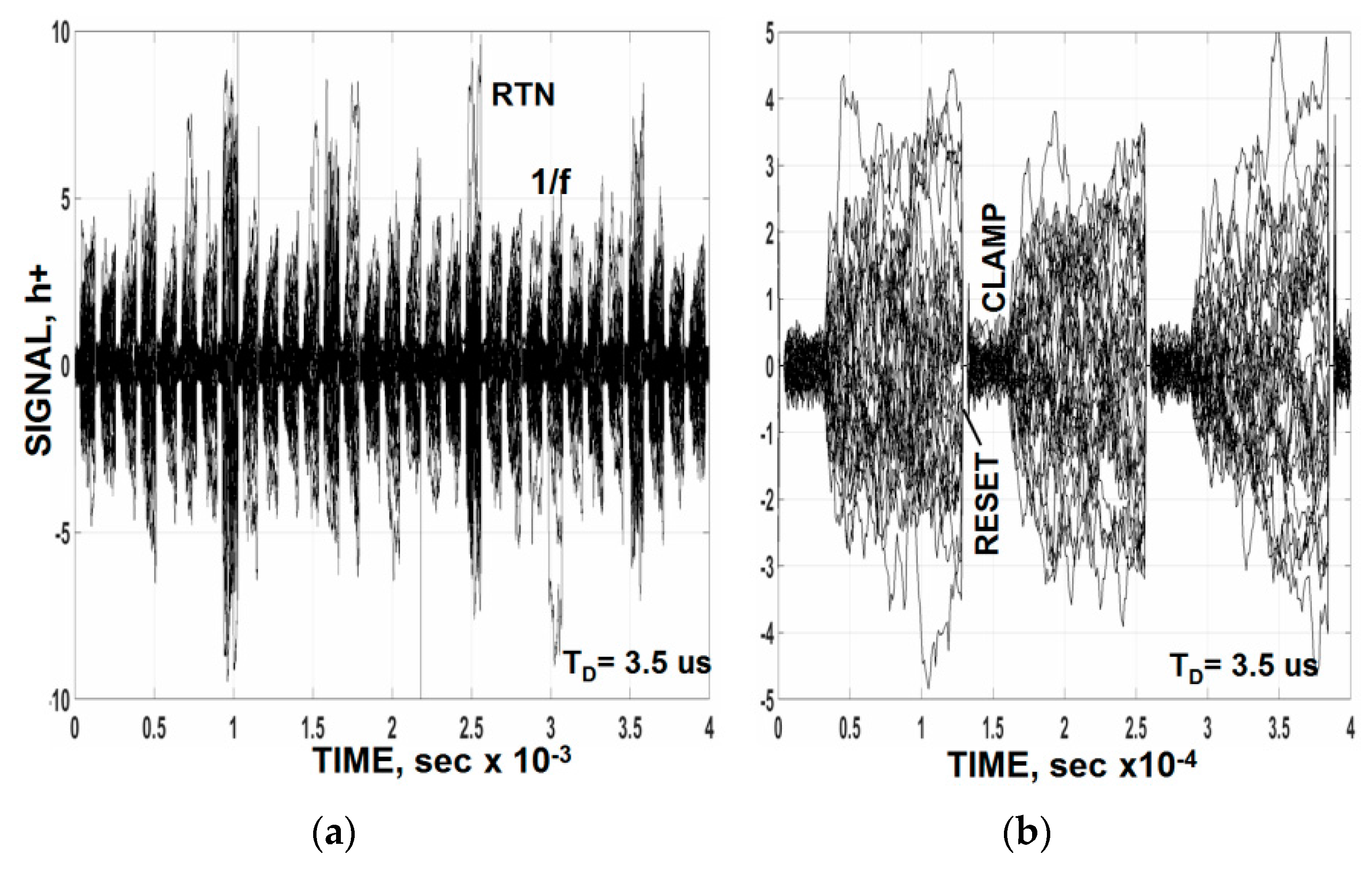
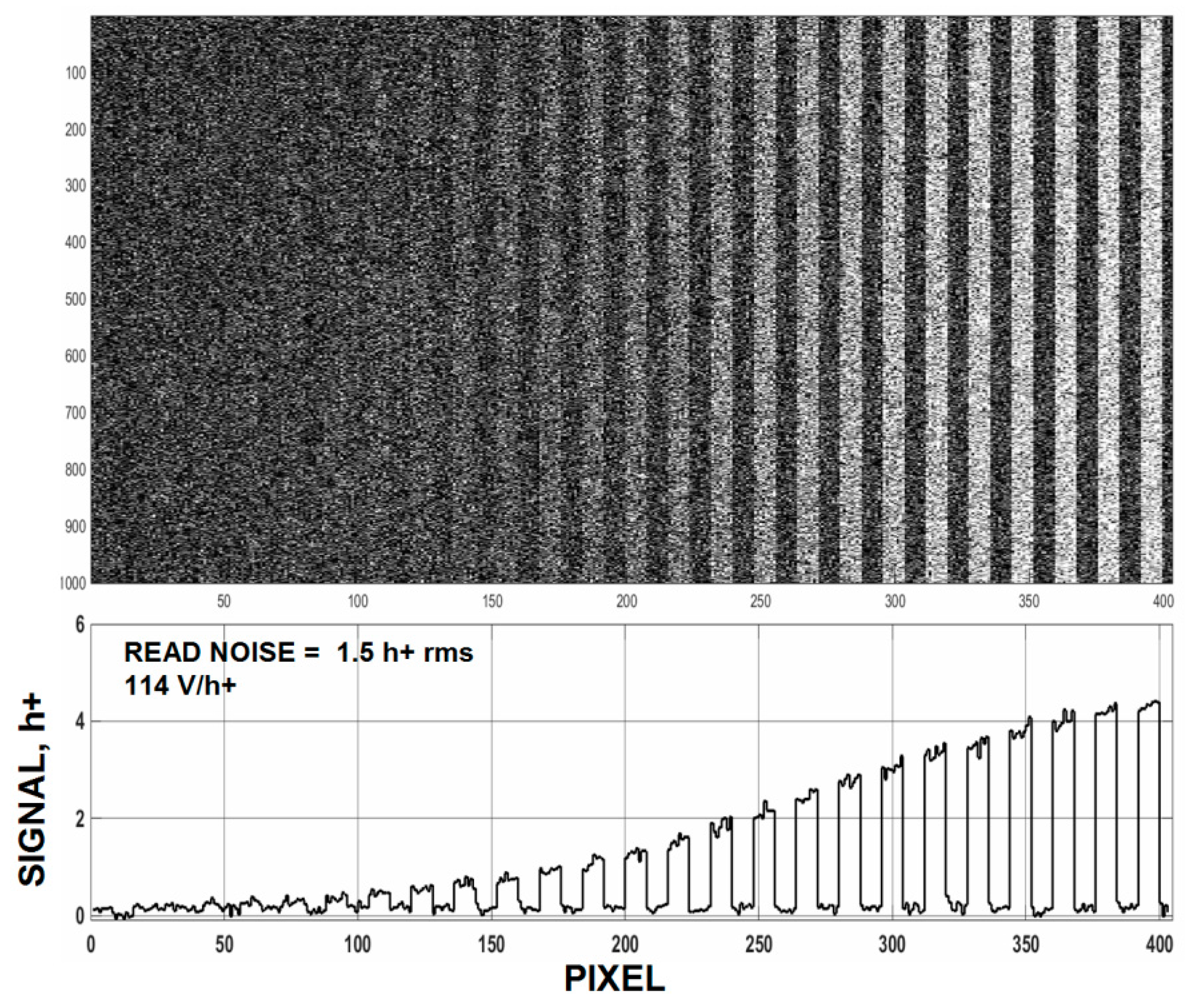
To demonstrate the claim above, stacked raw clamped dark video plots for a number of PMOS pixels is presented in
Figure 12a. The response shown is how the noise would appear on a high persistence oscilloscope before it enters an analog-to-digital converter with internal sample and hold. The magnified plot presented in
Figure 12b shows that timing starts by resetting and clamping the pixels’ video. The white noise seen in the clamp period is associated with the clamp switch (~0.1 h+). As one would expect 1/
f noise slowly increases after the clamp release due to lack of correlation.
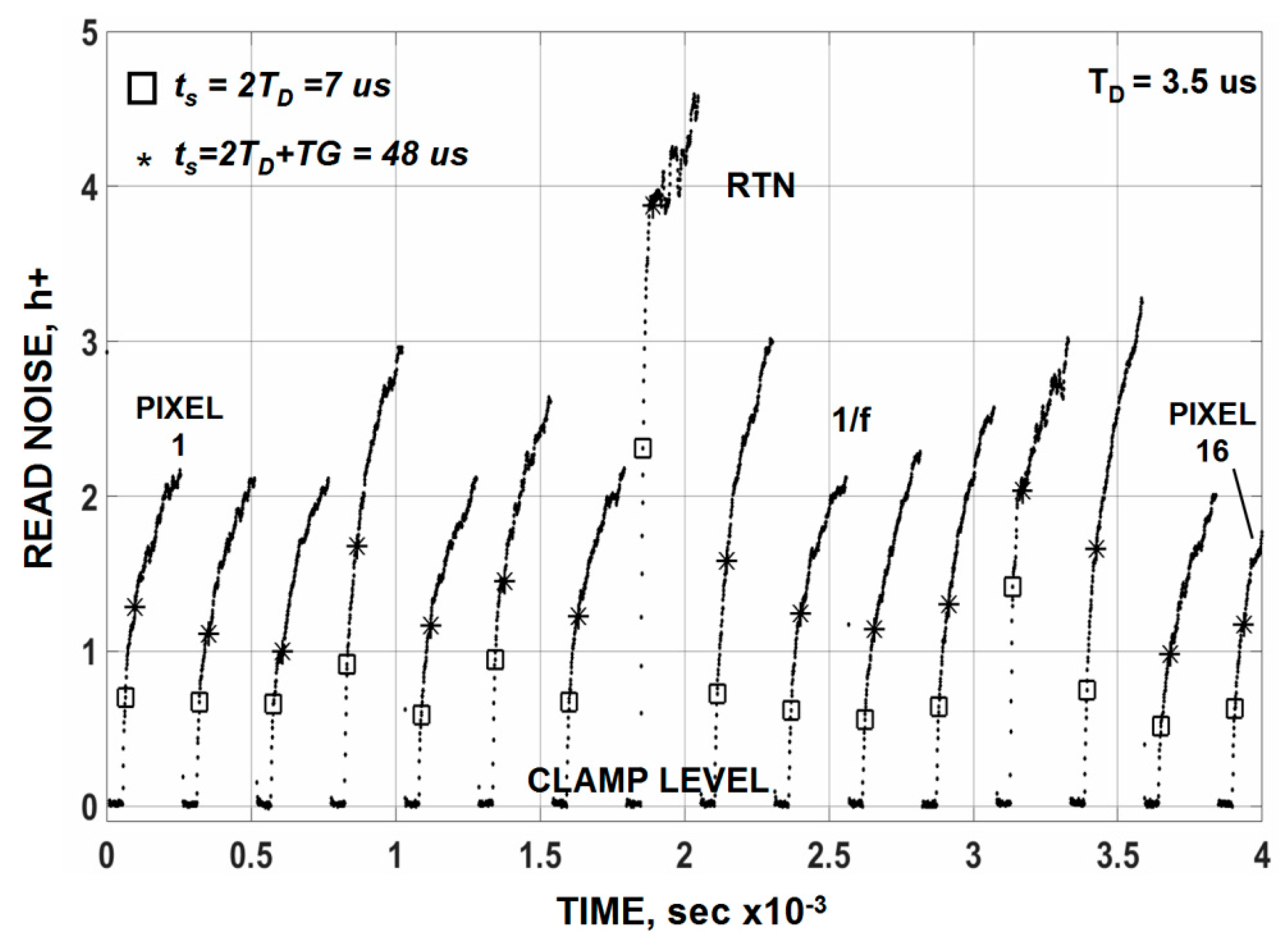
Figure 13 plots this read noise buildup for sixteen of the pixels. Ideally the video should be sampled as soon as the clamp is released after the required video τ
D settling time is satisfied for lowest noise performance (
i.e., t
s = 2τ
D = 7 µs in this case). This special timing condition is illustrated by the “squares” on the plot. An average noise level of ~0.9 h+ is measured for a row of 500 pixels of which the sixteen pixels are contained. The data points with “stars” include the pixel’s TG overhead time where a higher noise is measured (1.7 h+) because the 1/
f noise is less correlated. It should be also mentioned that averaging multiple samples in
Figure 13 does not help to reduce the read noise floor. This is because the samples are semi correlated and the noise within the sample increases for each new sample taken. As a result the noise increases with sample number at the same rate as the noise reduction offered by averaging (
i.e., N
1/2). It is very difficult to circumvent flicker noise presence for any signal processing scheme employed.
It is interesting to point out that using a 3T pixel for some applications can achieve a slightly lower noise than a 4T pixel simply because the 3T does not need to contend with TG overhead settling time. This assumes that the pixels are individually read out one by one by undergoing the entire exposure and CDS timing process (reset, clamp, flash expose and sample) before moving onto the next pixel. This approach is often used to test CMOS imagers including charge transfer pixels. Many figures in this paper are generated this manner to avoid dark current problems at room temperature.
Although not conventional, one can shorten the TG overhead time by sampling the video on the leading edge of the TG instead of the lagging edge. In fact sampling can be performed at any time throughout the TG clock period as long as the t
s = 2τ
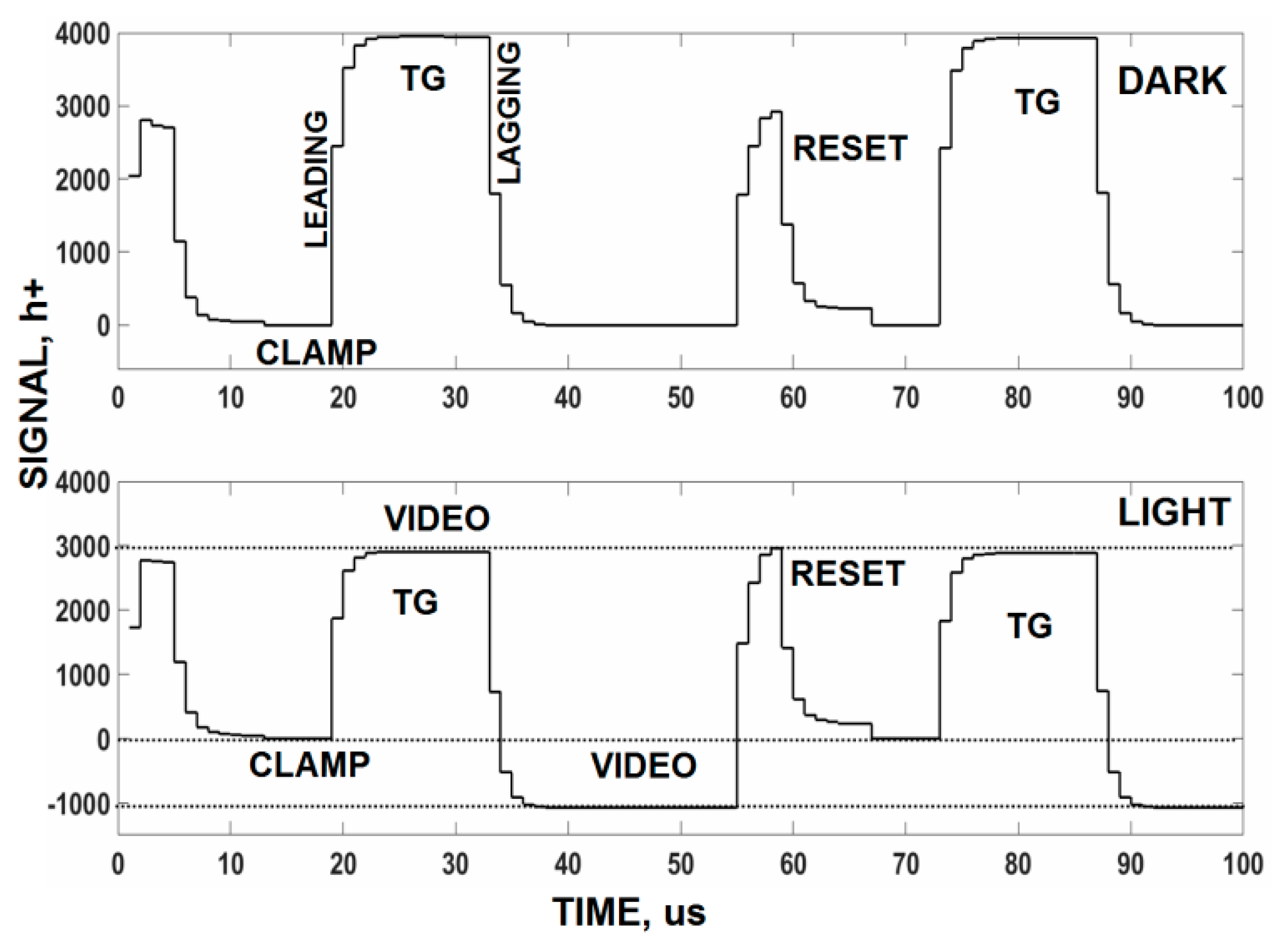
D settling time is satisfied.
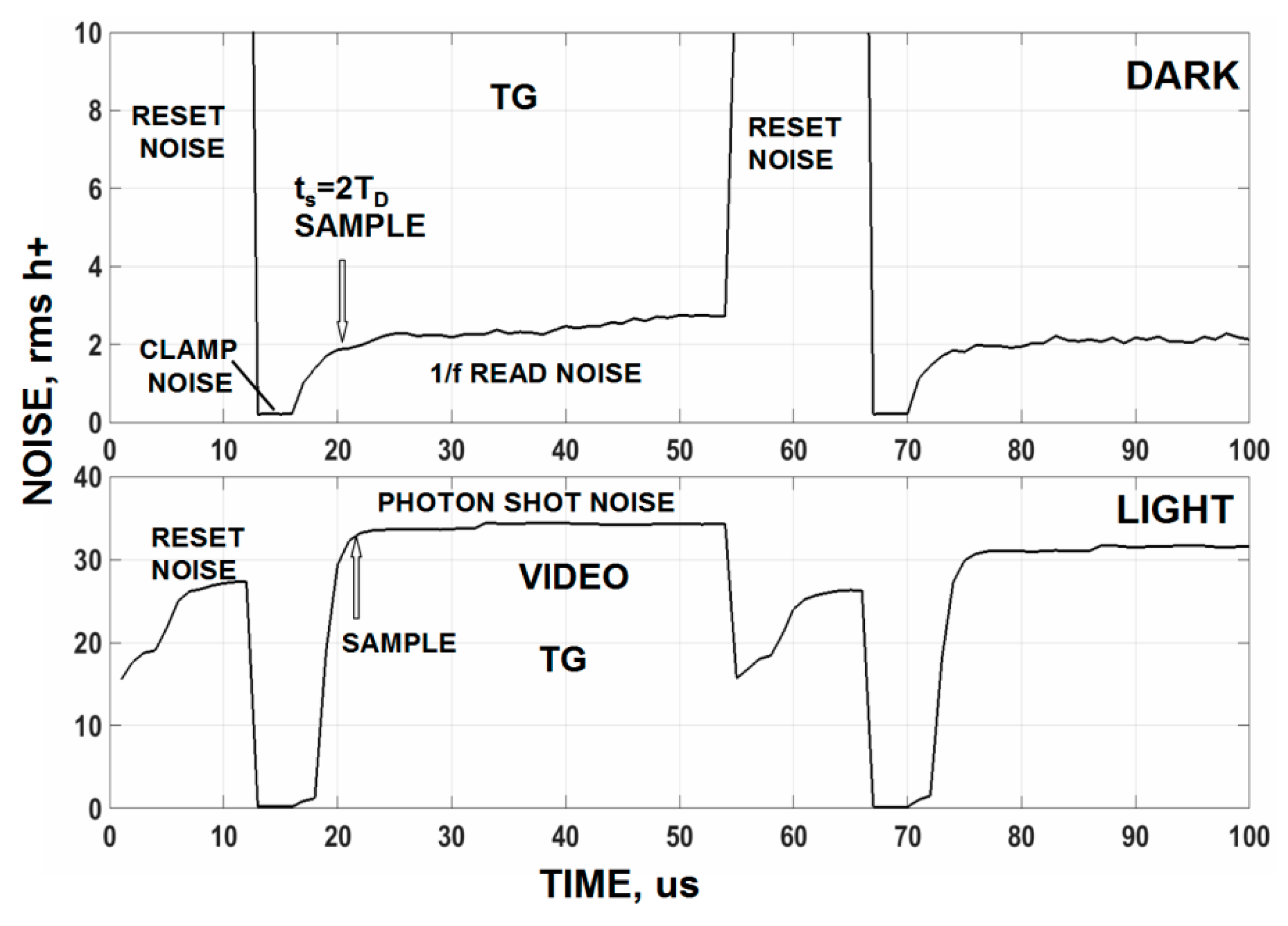
Figure 14 presents raw video traces taken under dark and light conditions. The traces show the reset clock feedthrough, clamp period, TG clock feedthrough and the downward change in video level to the light level applied.
Figure 15 is the corresponding noise measured for
Figure 14. Note after the clamp is released that the read noise increases due to correlation loss. The presence of a large TG clock feedthrough does not influence the noise measured because it only represents a changing offset which can be readily removed by a computer.
2.3. Conversion Gain
The conversion gain (V/carrier) depends on the various parasitic capacitances attached to the pixel’s floating diffusion SN besides the SF gate capacitance. It is our experience that the highest conversion gain realized does not bear the lowest average noise as long as the SF gate capacitance dominates. Instead an optimum SF size exists for lowest noise. Also in general, 1/f and SN sensitivity scale together for a large range of SF width and lengths. This strong relationship between 1/f and V/carrier has clearly been experienced when CCD and CMOS read noise performance is compared. The former technology typically has a considerably lower conversion gain than the latter yet both technologies in essence are limited to the same read noise floor (i.e., ~1 carrier rms). This outcome is because flicker noise is proportional to SF gate capacitance while the SN conversion gain is inversely proportional to it. SF MOSFET size and gate capacitance have grown smaller as imager technology improves but without a significant reduction in read noise.
2.4. Nondestructive Readout
Nondestructive floating gate readout schemes have worked in a straightforward fashion in producing sub carrier noise performance assuming there are no restrictions involving frame time requirements and operating temperature. The technology coined floating gate “Skipper” long ago can theoretical achieve any desired noise level as the read noise decreases by the square-root of the number of samples taken for each pixel [
2].
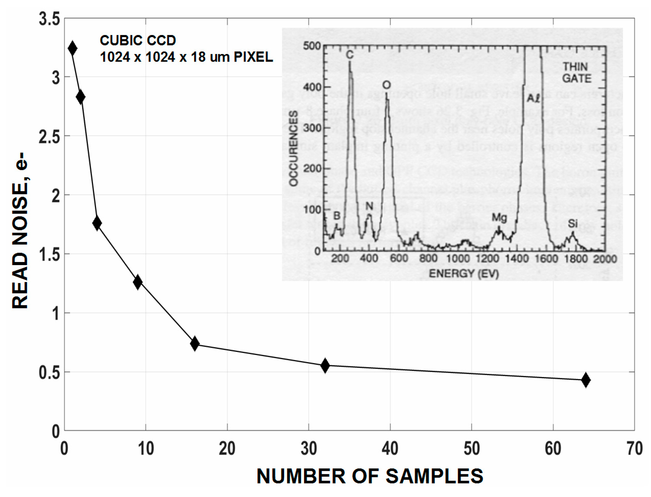
Figure 16 presents the read noise for a Skipper CCD where ~0.4 e
− is achieved with 64 samples beginning with a 3.25 e
− noise floor for a single sample [
1]. Unfortunately no attempt was made to count single visible photons with this imager since it was busy counting X-ray photons for a soft X-ray flight mission called Cosmic Unresolved Background Instrument (CUBIC). The SN conversion factor is quite low for the device (3 uV/ e
−) because of large parasitic SN and SF gate capacitances. More recent Skipper CMOS pixels have shown that the conversion gain for a floating gate and a floating diffusion are about the same. Hence, it may be possible for a 1 carrier noise Skipper device to achieve 0.3 e
− with nine samples using today’s fabrication technology without reducing 1/
f noise. These Skipper CMOS pixels were fabricated using a multi transfer buried channel gate process developed with Jazz Semiconductor for CMOSCCDs. No serious attempt has been made to characterize these pixels for photon counting use as of yet (only single sample data has been taken). The Skipper noise reduction approach was employed in the far past when the SN conversion was very low as sub micron fab technology did not exist. Today one can achieve the same 0.3 e
− noise floor with one sample with much higher conversion gain [
5].
4. Conclusions and Future Development
It could be tough going in lowering the “average” read noise substantially below 1 carrier rms because of the 1/f noise wall. CDS processing has been pushed to its limit in reducing noise from this source. Averaging multiple samples doesn’t help us since 1/f noise increases with time as a function of sample count increases. Using buried channel MOSFETS have been successful for reducing RTN but not for 1/f noise. Increasing the SN conversion gain is also restricted for the given design and process rules that must be followed. Although our SN conversion is presently limited to 160 uV/h+ there is still some wiggle room left in reducing parasitic capacitances associated with the TG and reset MOSFET that couple to the SN. However, the reduction won’t be that significant in that the SF capacitance currently dominates. Consequently, it appears the only means to lower read noise for us is to reduce 1/f noise head on.
Hence, future development will focus on 1/f reduction without knowing where it is coming from. Various trial and error approaches will be employed on a new runs currently being fabed (be it for mobility or GR reasons). For example one lot run contains deeper buried channel MOSFETs in hopes to see a 1/f noise change. Special attention is being given to punch-through issues which usually emerge with buried channel use. Also in order to maximize the surface barrier potential for a buried device the SN must be reset to a SF gate bias voltage that is close as possible to substrate potential. Doing so will reduce dynamic range but the foremost objective behind these experiments is to locate the 1/f noise source without much regard to using the pixel in practice.
Experiments involving implants associated with the wells which contain the pixel MOSFETs are being fabricated. We can do this because the pixel implants are derived from custom reticules and independent from the standard
n and
p_wells used for support circuitry. As mentioned above reducing the doping concentration near the surface could lead to a more uniform current flow with less fluctuation. For example, experimental pixels being fabricated will include a single “minimum implant dose” SF MOSFET. Possibly there will be a 1/
f noise change since this implant recipe is considerably different than the 3 implant process being used now that is intended for high speed digital MOSFETs. Also further thermal annealing is being incorporated to better activate the pixel wells. The sub carrier noise pixels in
Figure 5 and
Figure 6 were fabricated with a past 0.25 µm CMOS process which is known to produce lower 1/
f noise than the 0.18 um process applied today. The 0.25 µm process used a longer thermal anneal cycle. In addition a very long and greater temperature anneal at the very start of the process is being tried to make sure the implants are fully activated.
Native MOSFETs of various geometries are also being fabricated. The native MOSFET is known to have lower 1/
f noise given that the SF channel doping is the epitaxial silicon [
8]. Our epi silicon resistivity varies widely from 10 to 1000 ohm-cm, and hence, we should see a 1/
f noise change. The experiment will also include baseline MOSFETs with the same geometries as the natives in order to compare 1/
f noise levels.
Lastly we are trying a proprietary non-imaging gate oxide process offered by Jazz Semiconductor that claims to lower MOSFET 1/f RTN noise by 4 to 5 times compared to 0.18 um processing that is used now. All 1/f noise reduction approaches above will need to determine the optimum SF geometry for lowest noise performance.

