
A Fast Multiple Sampling Method for Low-Noise CMOS Image Sensors With Column-Parallel 12-bit SAR ADCs

Abstract
:1. Introduction
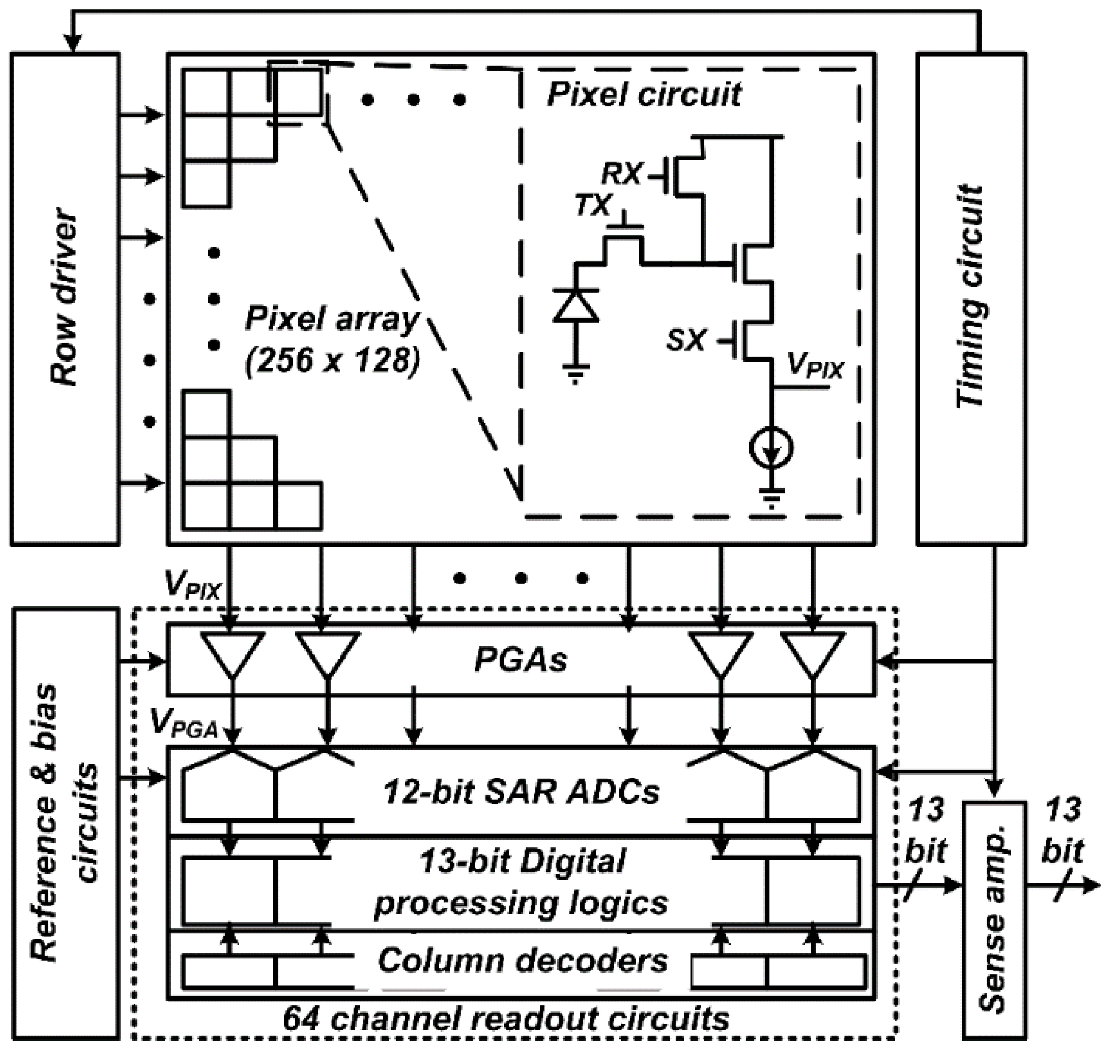
2. CIS Architecture
2.1. Block Diagram


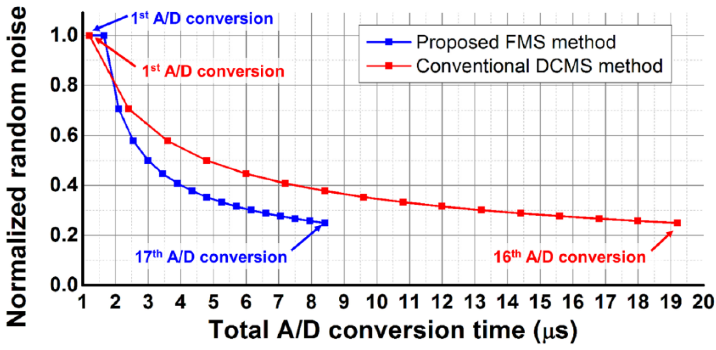
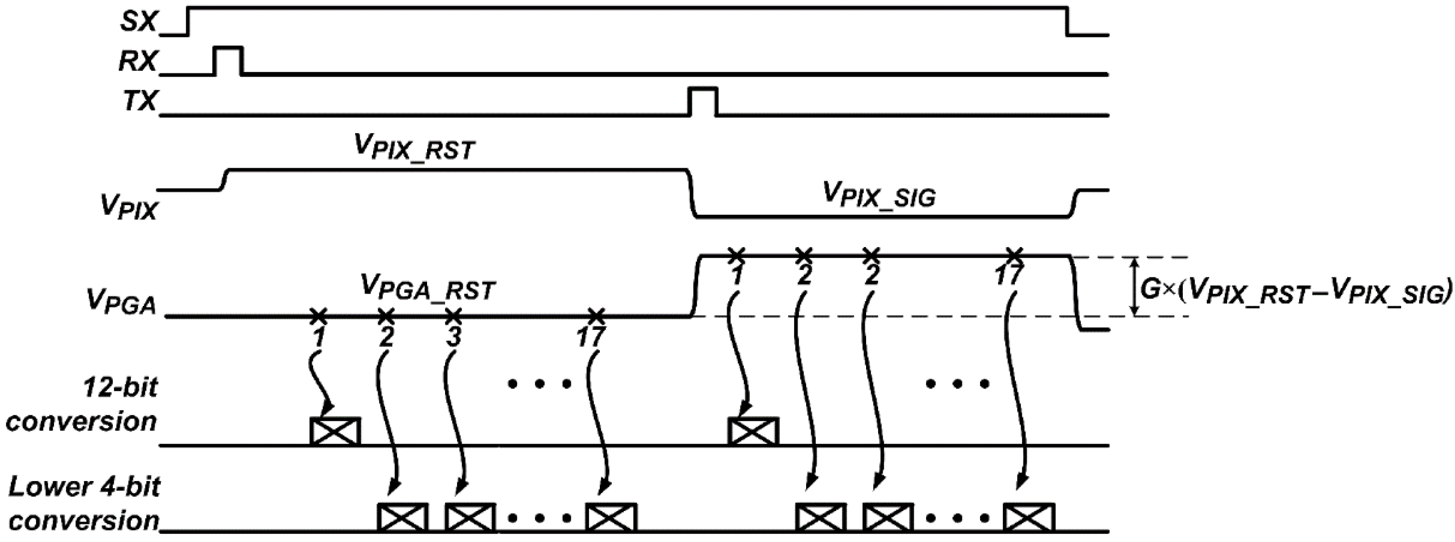
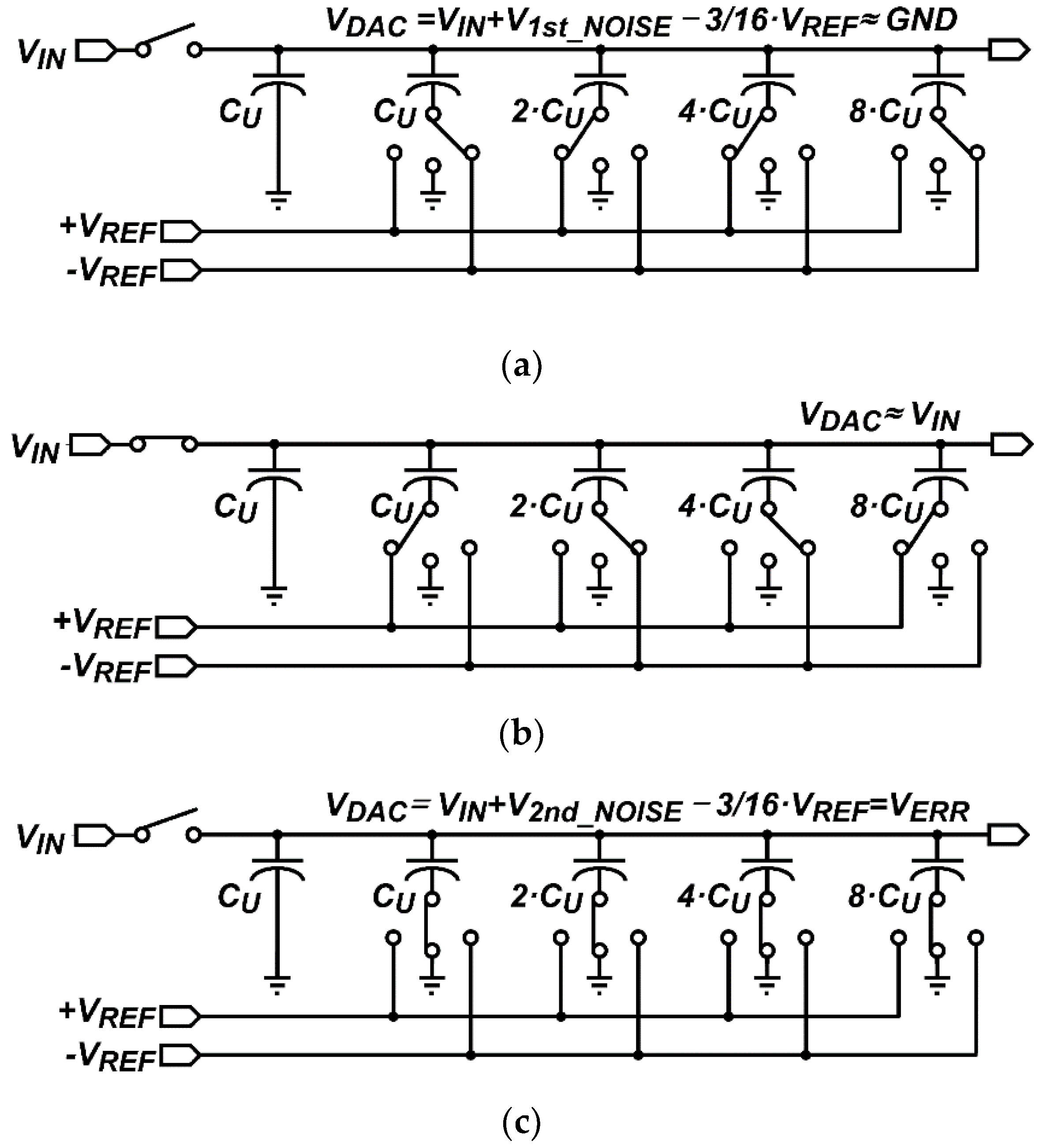
2.2. Operating Principle of the Proposed FMS Method


3. Circuit Implementation
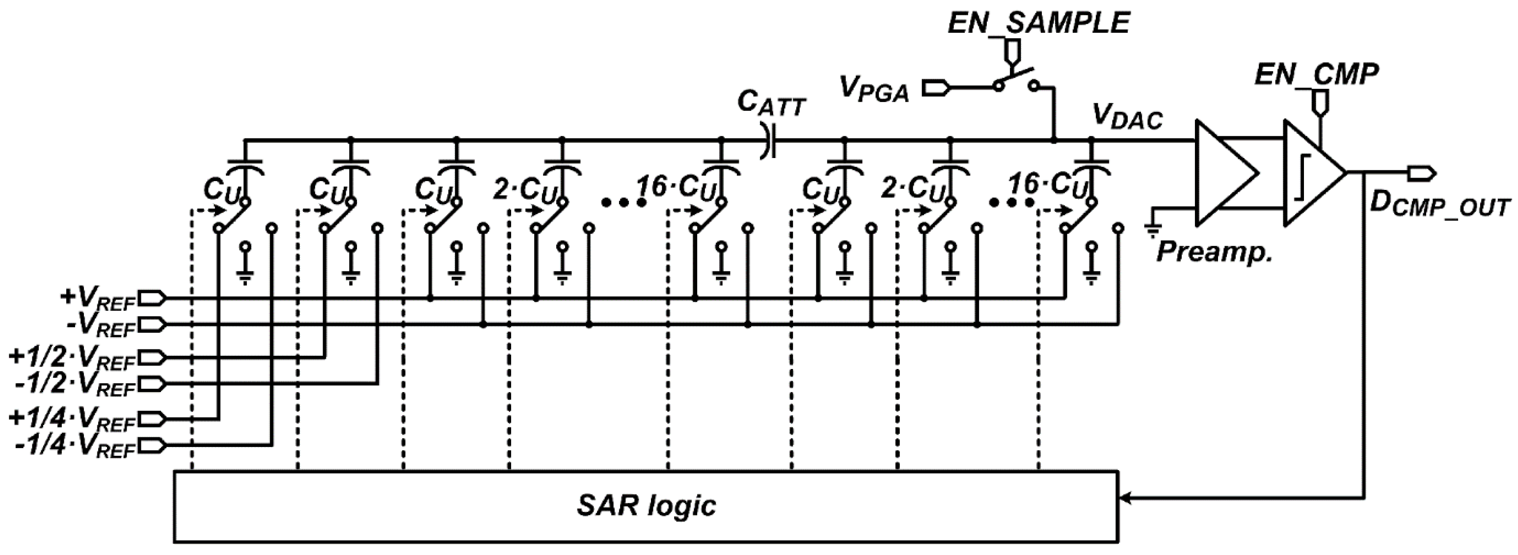
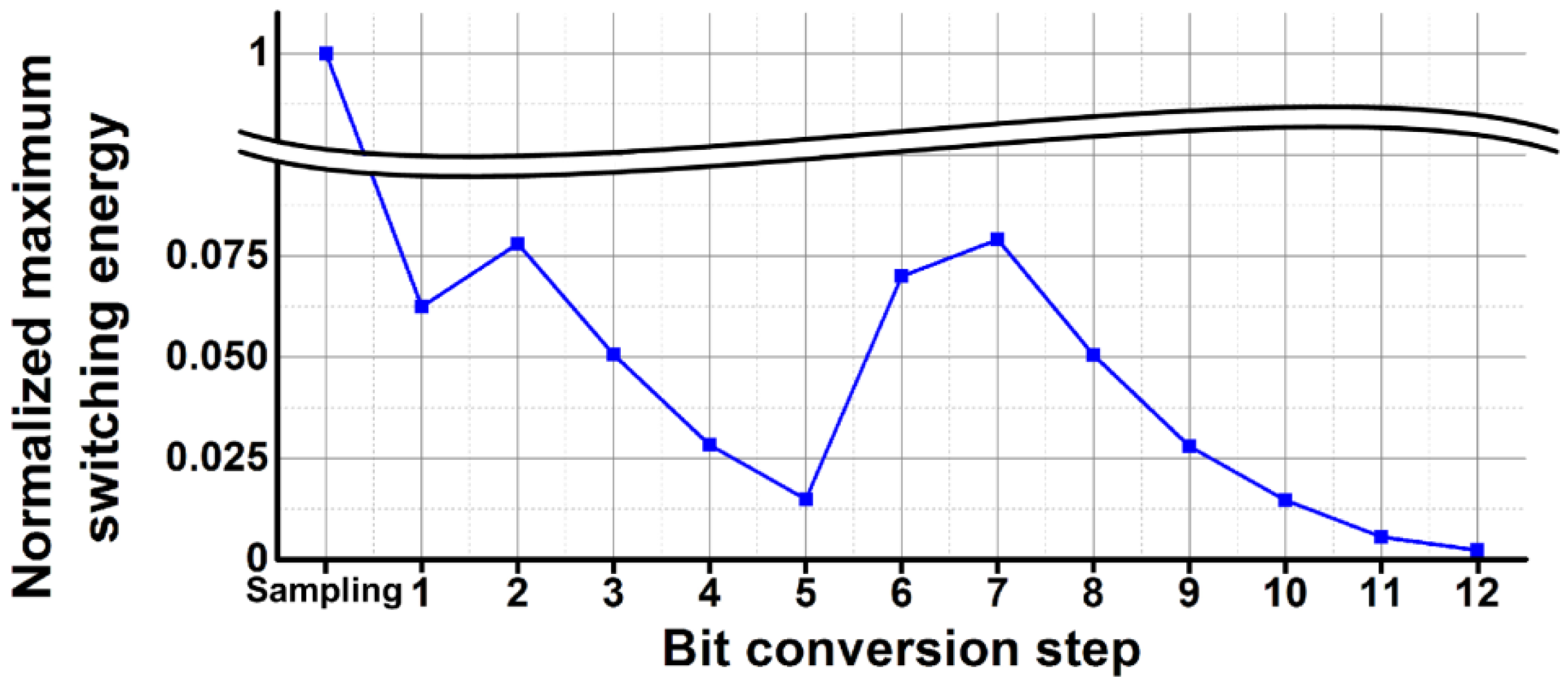
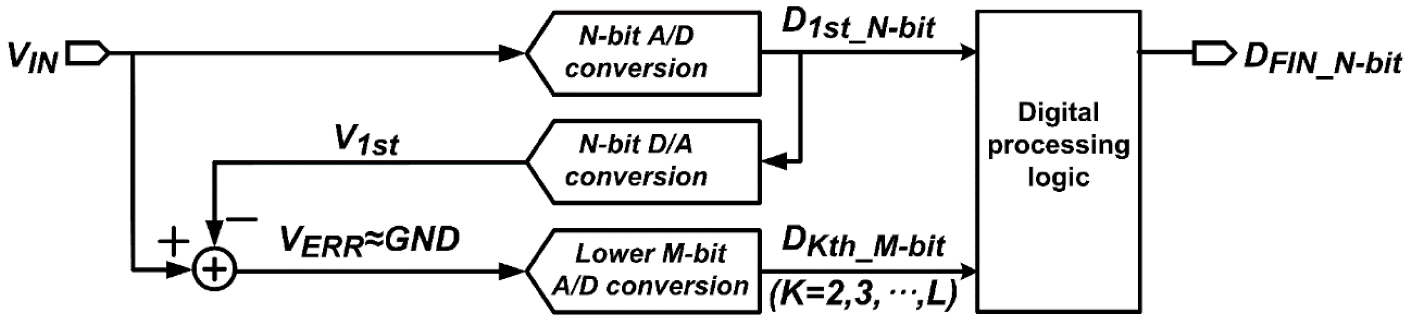
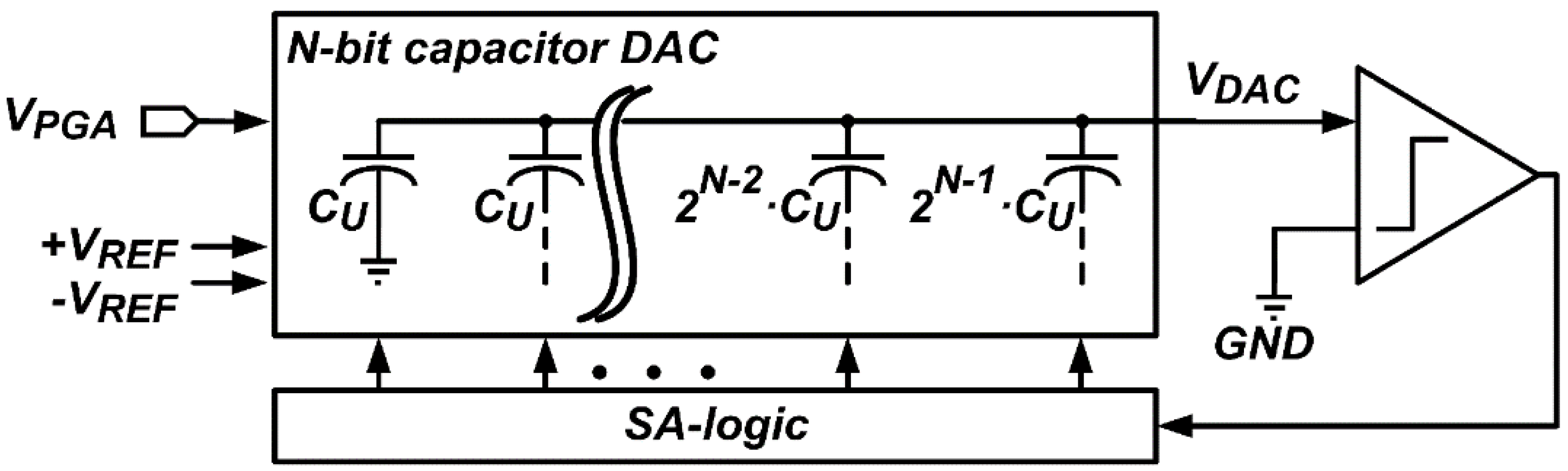
3.1. Design of 12-bit SAR ADC Using the Proposed FMS Method
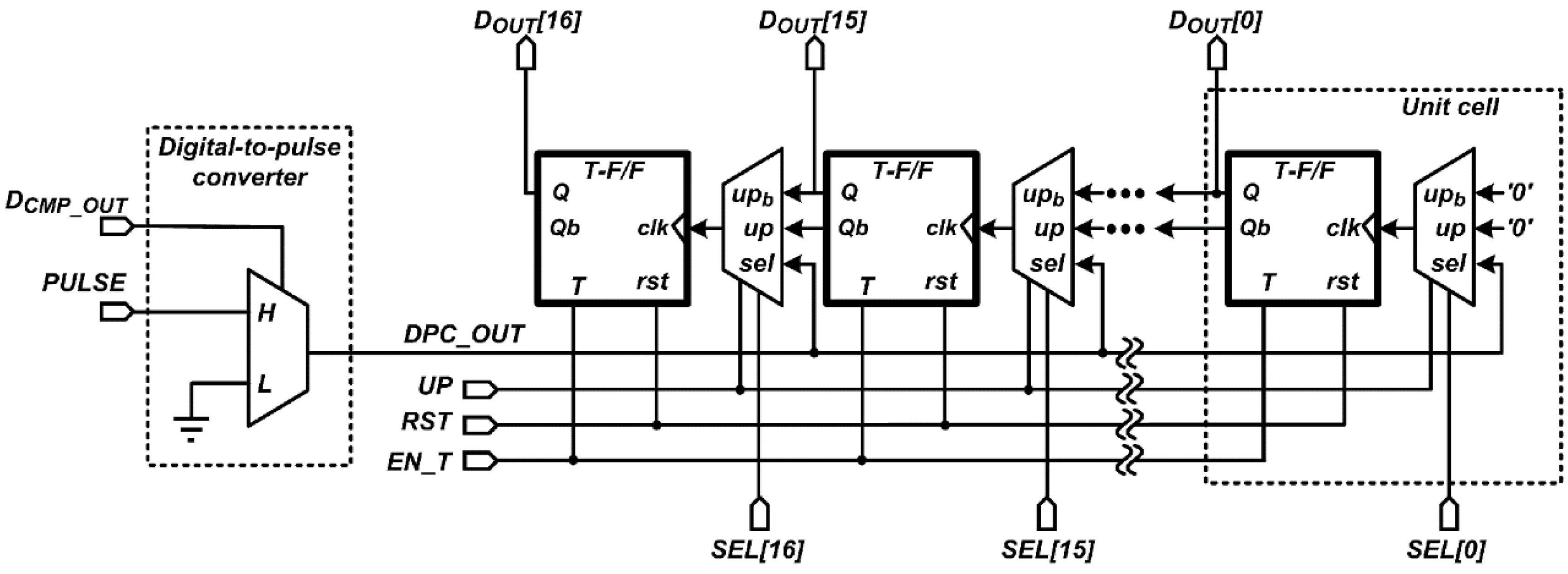
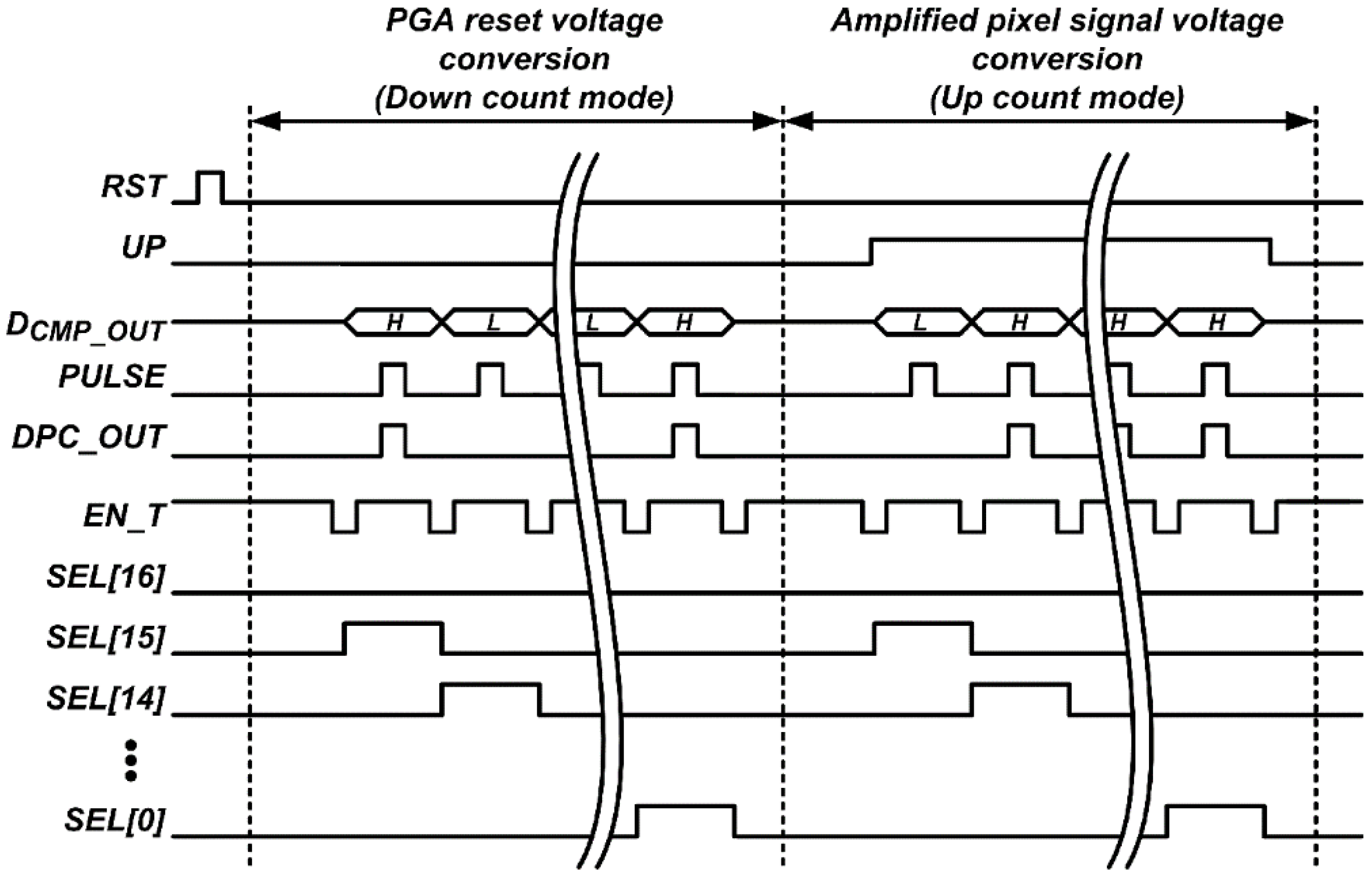
3.2. Design of Digital Processing Logic


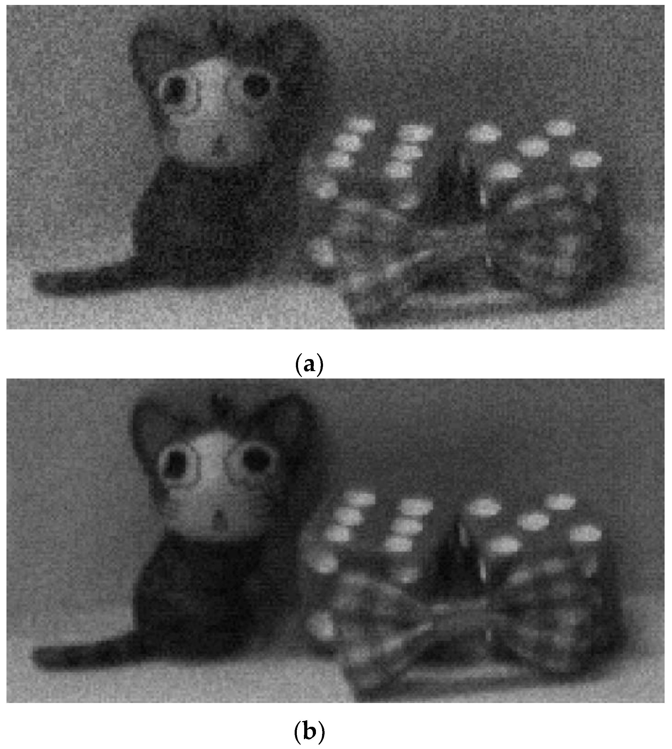
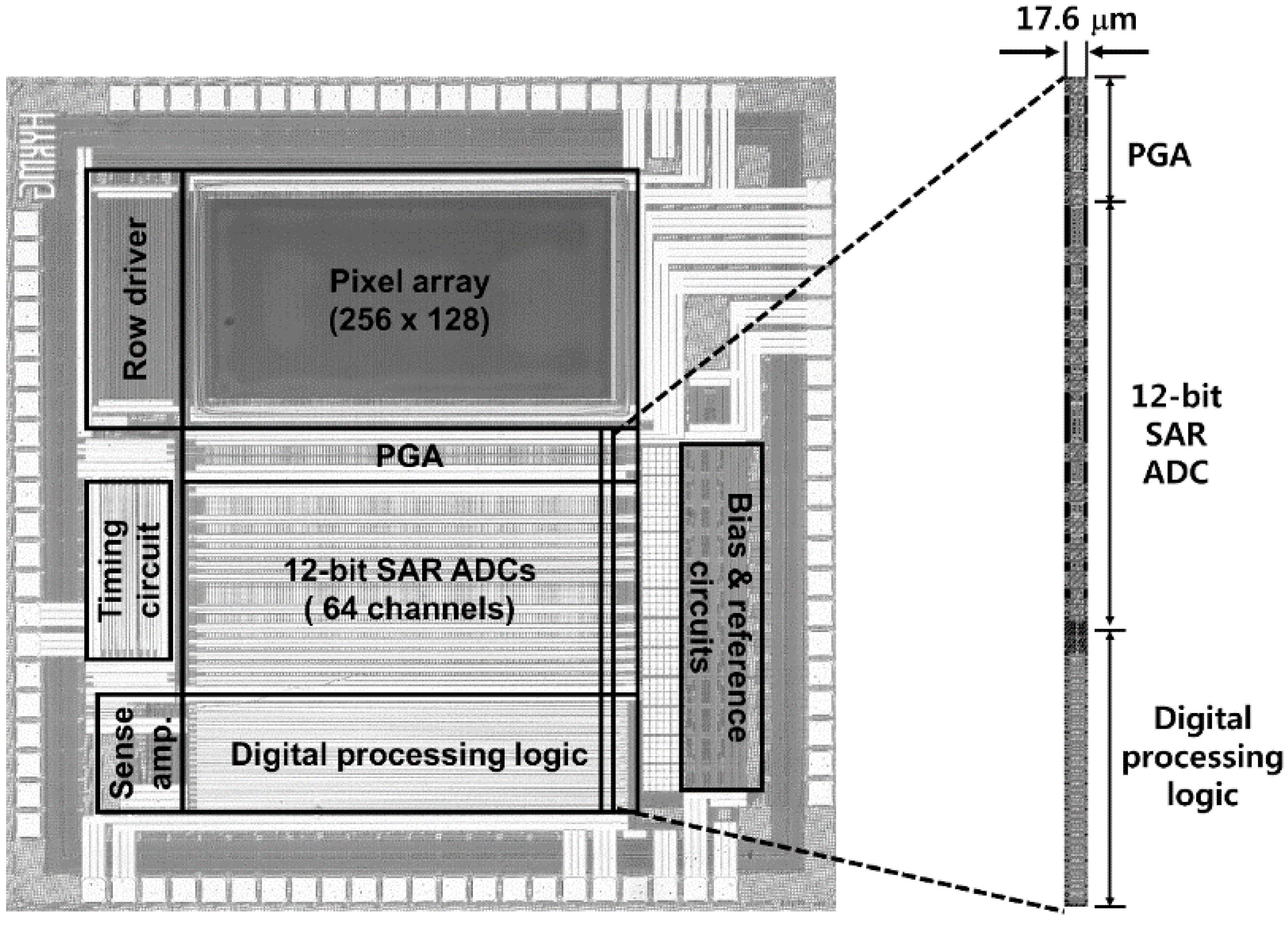
4. Experimental Results


| Parameter | Value |
|---|---|
| Process | 0.18 μm 1-poly 4-metal CMOS process |
| Supply voltage | 2.8 V/1.8 V |
| Chip size | 2.35 mm × 2.35 mm |
| Pixel array size | 256 (H) × 128 (V) |
| Maximum frame rate | 90 frames/s |
| Pixel size | 4.4 μm × 4.4 μm |
| Conversion gain | 60 μV/e− |
| Full well capacity | 11.4 ke− |
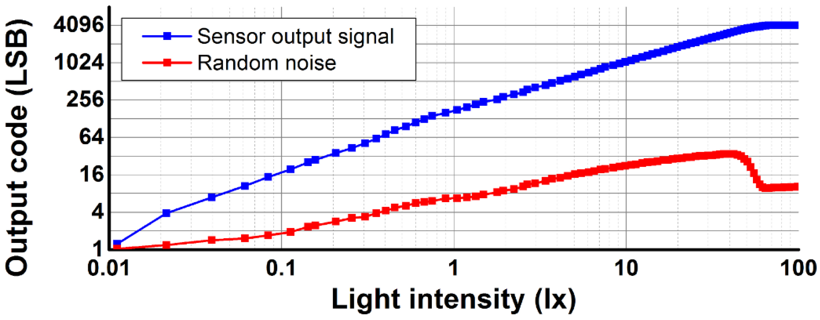
| Sensitivity | 6.2 V/lx·s |
| Column FPN at dark | 0.17 LSB |
| SNR | 39.2 dB |
| Dynamic range | 68.1 dB |
| ADC input range | 0.9 V |
| ADC resolution | 12-bit |
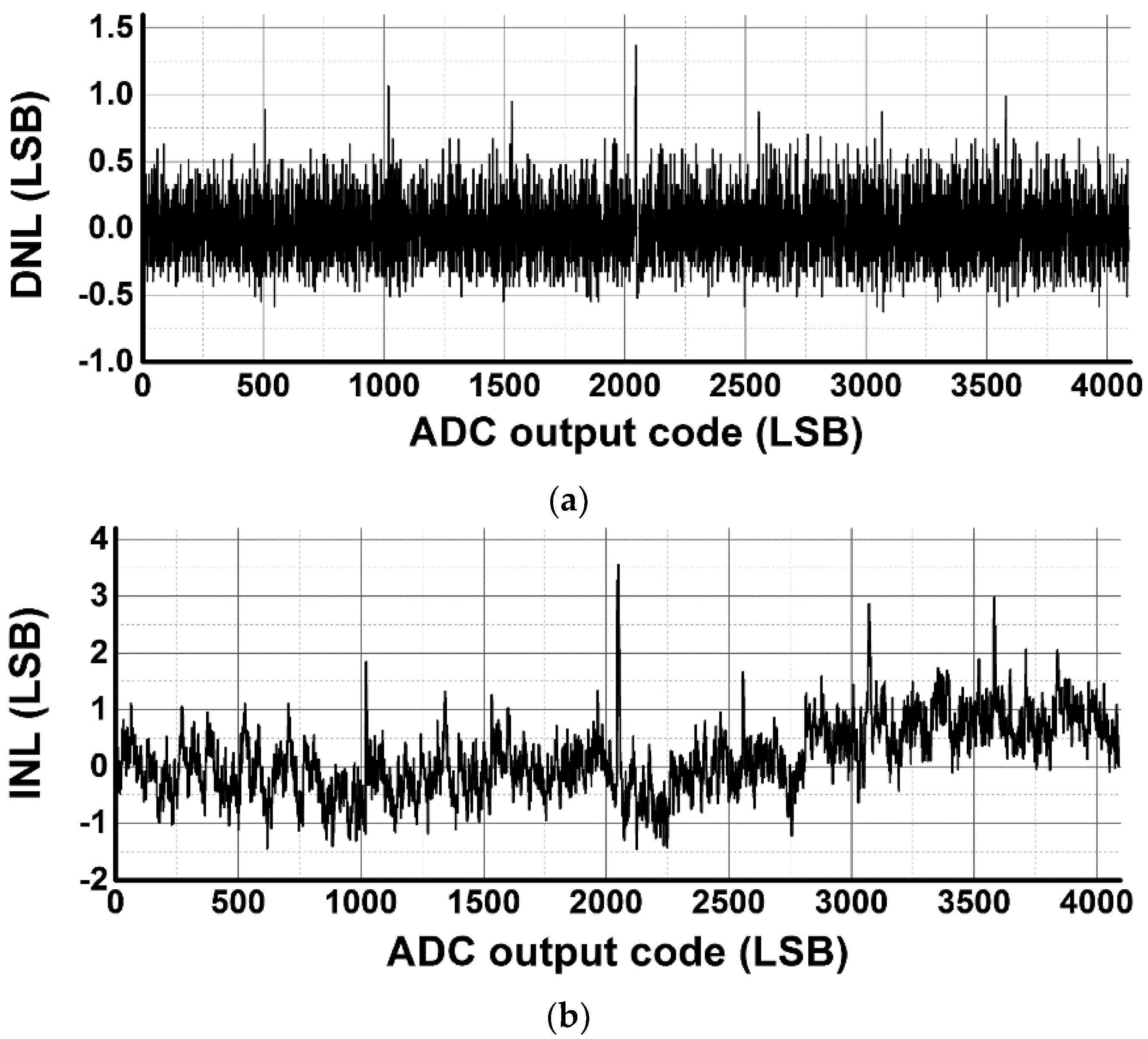
| DNL | −0.62/+1.37 LSB |
| INL | −1.42/+3.55 LSB |
| Power consumption | 4.4 mW |
| Parameter | This Work | [3] | [12] | [13] | [14] | [20] | [21] |
|---|---|---|---|---|---|---|---|
| Pixel array size | 256 × 128 | 4112 × 2186 | 1280 × 800 | 920 × 256 | 644 × 488 | 54 × 50 | 64 × 45 |
| Frame rate (frame/s) | 90 | 60 | 35 | 9 | 120 | 7.4 | 21.2 |
| ADC Resolution (bit) | 12 | 14 | 11 | 9 | 14 | 10 | 8 |
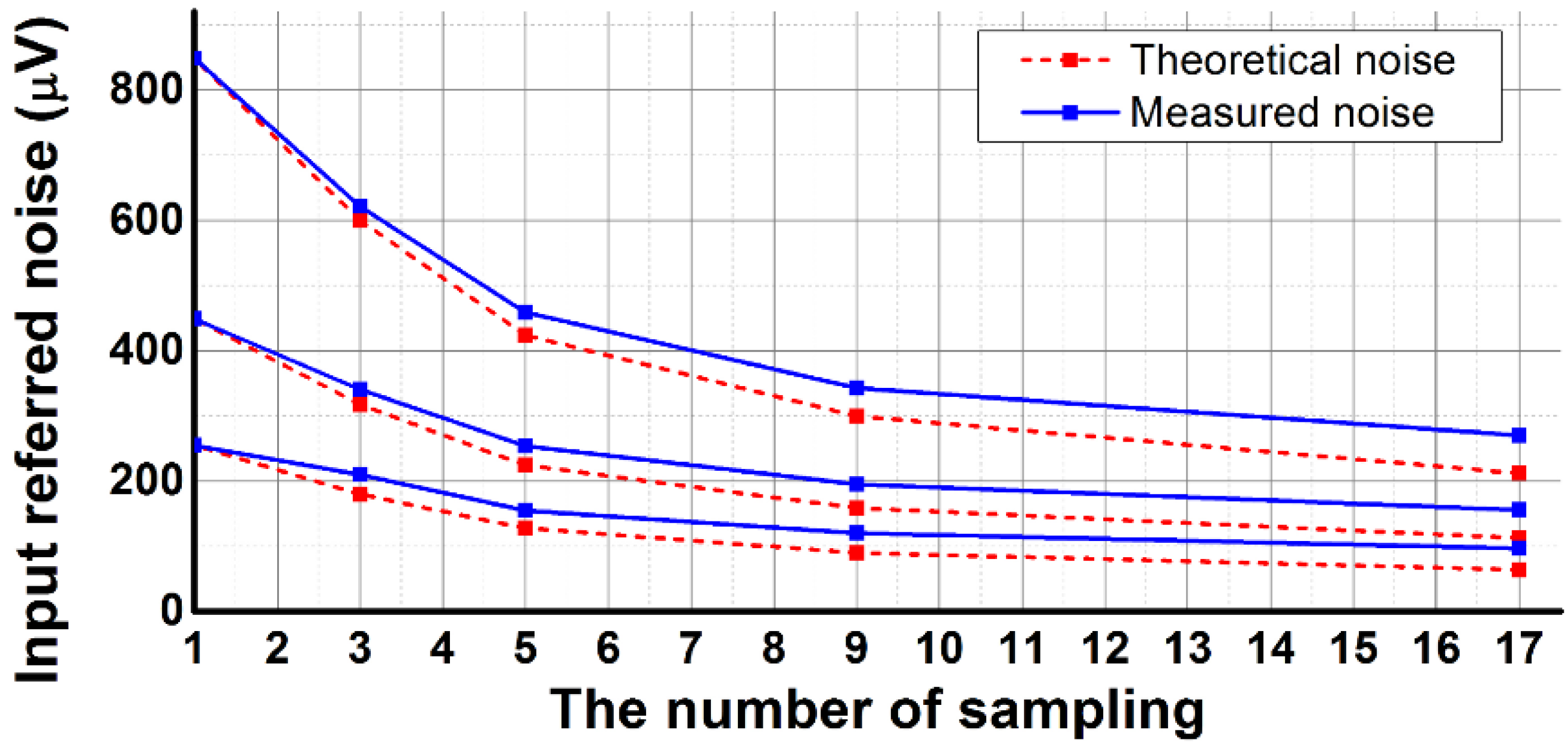
| Random noise (μVrms) | 96.5 (0.44 LSB) | 130.5 | 1500 | 5300 | 83 | 0.98 LSB | 0.5 LSB |
| Power consumption (mW) | 4.4 | 108.5 | 40 | 1.1 | 78 | 0.014 | 0.021 |
| FOM (μV·nJ) | 145 | 265 | 1674 | 28147 | 171 | - | - |
5. Conclusions
Acknowledgments
Author Contributions
Conflicts of Interest
References
- Kawai, N.; Kawahito, S. Noise analysis of high-gain, low-noise column readout circuits for CMOS image sensors. IEEE Trans. Electron. Devices 2004, 51, 185–194. [Google Scholar] [CrossRef]
- Takahashi, H.; Noda, T.; Matsuda, T.; Watanabe, T.; Shinohara, M.; Endo, T.; Takimoto, S.; Mishima, R.; Nishimura, S.; Sakurai, K.; et al. A 1/2.7 inch low-noise CMOS image sensor for full HD camcorders. In Proceedings of the IEEE International Solid-State Circuits Conference. Digest of Technical Papers, San Francisco, CA, USA, 11–15 February 2007; pp. 510–511.
- Matsuo, S.; Bales, T.J.; Shoda, M.; Osawa, S.; Kawamura, K.; Andersson, A.; Haque, M.; Honda, H.; Almond, B.; Mo, Y.; et al. 8.9-megapixel video image sensor with 14-b column parallel SA-ADC. IEEE Trans. Electron. Devices 2009, 56, 2380–2389. [Google Scholar] [CrossRef]
- Suh, S.; Itoh, S.; Aoyama, S.; Kawahito, S. Column-parallel correlated multiple sampling circuits for CMOS image sensors and their noise reduction effects. Sensors 2010, 10, 9139–9154. [Google Scholar] [CrossRef] [PubMed]
- Chen, Y.; Xu, Y.; Mierop, A.J.; Theuwissen, A.J.P. Column parallel digital correlated multiple sampling for low-noise CMOS image sensors. IEEE Sens. J. 2012, 12, 793–799. [Google Scholar] [CrossRef]
- Lim, Y.; Koh, K.; Kim, K.; Yang, H.; Kim, J.; Jeong, Y.; Lee, S.; Lee, H.; Lim, S.-H.; Han, Y.; et al. A 1.1 e-temporal noise 1/3.2-inch 8 Mpixel CMOS image sensor using pseudo-multiple sampling. In Proceedings of the IEEE International Solid-State Circuits Conference. Digest of Technical Papers, San Fransisco, CA, USA, 7–11 February 2010; pp. 396–397.
- Fowler, A.; Gatley, I. Noise reduction strategy for hybrid IR focal plane arrays. In Proceedings of the Infrared Sensors: Detectors, Electronics, and Signal Processing (SPIE), San Diego, CA, USA, 21 July 1991; pp. 127–133.
- Eltoukhy, H.; Salama, K.; El-Gamal, A. A 0.18 μm CMOS Bioluminescence Detection Lab-on-Chip. IEEE J. Solid State Circuits 2006, 41, 651–662. [Google Scholar] [CrossRef]
- Chae, Y.; Cheon, J.; Lim, S.; Kwon, M.; Yoo, K.; Jung, W.; Lee, D.-H.; Ham, S.; Han, G. A 2.1 M pixels, 120 frame/s CMOS image sensor with column-parallel ΔΣ ADC architecture. IEEE J. Solid State Circuits 2011, 46, 236–247. [Google Scholar] [CrossRef]
- Seo, M.-W.; Suh, S.-H.; Iida, T.; Takasawa, T.; Isobe, K.; Watanabe, T.; Itoh, S.; Yasutomi, K.; Kawahito, S. A low-noise high intrascene dynamic range CMOS image sensor with a 13 to 19b variable-resolution column-parallel folding-integration/cyclic ADC. IEEE J. Solid State Circuits 2012, 47, 272–283. [Google Scholar] [CrossRef]
- Kim, J.-H.; Jung, W.-K.; Lim, S.-H.; Park, Y.-J.; Choi, W.-H.; Kim, Y.-J.; Kang, C.-E.; Shin, J.-H.; Choo, K.-J.; Lee, W.-B.; et al. A 14b extended counting ADC implemented in a 24 Mpixel APS-C CMOS image sensor. In Proceedings of the IEEE International Solid-State Circuits Conference. Digest of Technical Papers, San Francisco, CA, USA, 19–23 February 2012; pp. 390–392.
- Chen, D.G.; Tang, F.; Bermak, A. A Low-Power Pilot-DAC Based Column Parallel 8b SAR ADC With Forward Error Correction for CMOS Image Sensors. IEEE Trans. Circuits. Syst. I Reg. Pap. 2013, 60, 2572–2583. [Google Scholar] [CrossRef]
- Chen, D.G.; Tang, F.; Law, M.K.; Zhong, X.; Bermak, A. A 64fJ/step 9-bit SAR ADC array with forward error correction and mixedsignal CDS for CMOS image sensors. IEEE Trans. Circuits. Syst. I Reg. Pap. 2014, 61, 3085–3092. [Google Scholar] [CrossRef]
- Kim, J.-B.; Hong, S.-K.; Kwon, O.-K. A Low-Power CMOS Image Sensor With Area-Efficient 14-bit Two-Step SA ADCs Using Pseudomultiple Sampling Method. IEEE Trans. Circuits Syst. II 2015, 62, 451–455. [Google Scholar] [CrossRef]
- Ginsburg, B.P.; Chandrakasan, A.P. An Energy-Efficient Charge Recycling Approach for a SAR Converter With Capacitive DAC. In Proceedings of the IEEE International Symposium on Circuits and Systems, Kobe, Japan, 23–26 May 2005; pp. 184–187.
- White, M.H.; Lampe, D.R.; Blaha, F.C.; Mack, I.A. Charactarization of surface channel CCD image arrays at low light levels. IEEE J. Solid State Circuits 1974, 9, 1–13. [Google Scholar] [CrossRef]
- Gowda, S.M.; Shin, H.J.; Wong, H.-S.P.; Xiao, P.H.; Yang, J. Image sensor with direct digital correlated sampling. US Patent #6,115,066, 5 September 2000. [Google Scholar]
- Park, J.-H.; Aoyama, S.; Watanabe, T.; Isobe, K.; Kawahito, S. A High-Speed Low-Noise CMOS Image Sensor With 13-b Column-Parallel Single-Ended Cyclic ADCs. IEEE Trans. Electron. Devices 2009, 56, 2414–2422. [Google Scholar] [CrossRef]
- Han, L.; Yao, S.; Xu, J.; Xu, C.; Gao, Z. Analysis of incomplete charge transfer effects in a CMOS image sensor. J. Semicond. 2013, 34, 054009. [Google Scholar] [CrossRef]
- Cevik, I.; Ay, S. An Ultra-Low Power Energy Harvesting and Imaging (EHI) Type CMOS APS Imager with Self-Power Capability. IEEE Trans. Circuits Syst. I 2015, 62, 2177–2186. [Google Scholar] [CrossRef]
- Ay, S. A 1.32pW/frame.pixel 1.2V CMOS Energy Harvesting and Imaging (EHI) APS Imager. In Proceedings of the 2011 International Solid- State Circuits Conference (ISSCC), San Francisco, CA, USA, 20–24 February 2011; pp. 116–117.
© 2015 by the authors; licensee MDPI, Basel, Switzerland. This article is an open access article distributed under the terms and conditions of the Creative Commons by Attribution (CC-BY) license (http://creativecommons.org/licenses/by/4.0/).
Share and Cite
Kim, M.-K.; Hong, S.-K.; Kwon, O.-K. A Fast Multiple Sampling Method for Low-Noise CMOS Image Sensors With Column-Parallel 12-bit SAR ADCs. Sensors 2016, 16, 27. https://doi.org/10.3390/s16010027
Kim M-K, Hong S-K, Kwon O-K. A Fast Multiple Sampling Method for Low-Noise CMOS Image Sensors With Column-Parallel 12-bit SAR ADCs. Sensors. 2016; 16(1):27. https://doi.org/10.3390/s16010027
Chicago/Turabian StyleKim, Min-Kyu, Seong-Kwan Hong, and Oh-Kyong Kwon. 2016. "A Fast Multiple Sampling Method for Low-Noise CMOS Image Sensors With Column-Parallel 12-bit SAR ADCs" Sensors 16, no. 1: 27. https://doi.org/10.3390/s16010027
APA StyleKim, M.-K., Hong, S.-K., & Kwon, O.-K. (2016). A Fast Multiple Sampling Method for Low-Noise CMOS Image Sensors With Column-Parallel 12-bit SAR ADCs. Sensors, 16(1), 27. https://doi.org/10.3390/s16010027