
A High Performance Delta-Sigma Modulator for Neurosensing

Abstract
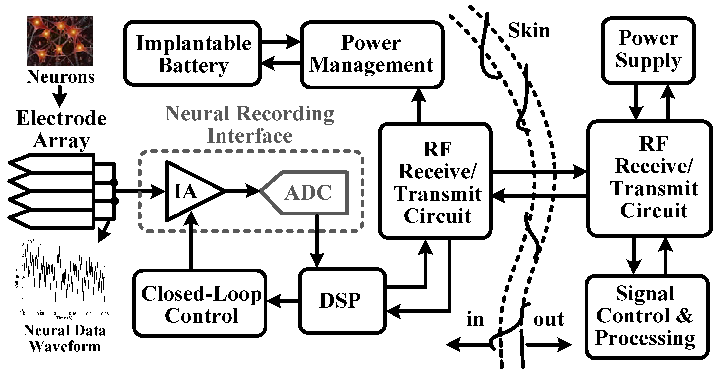
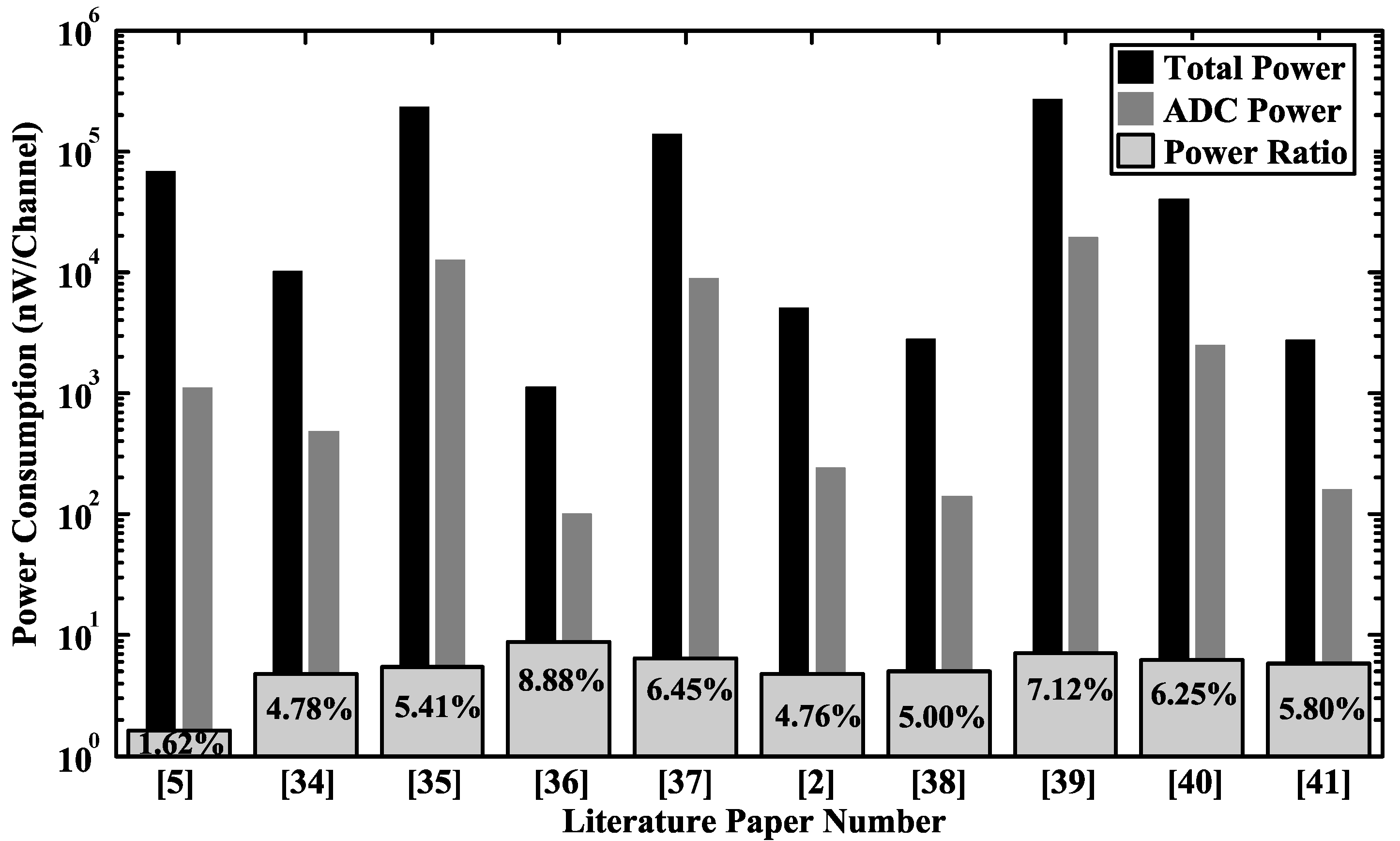
:1. Introduction

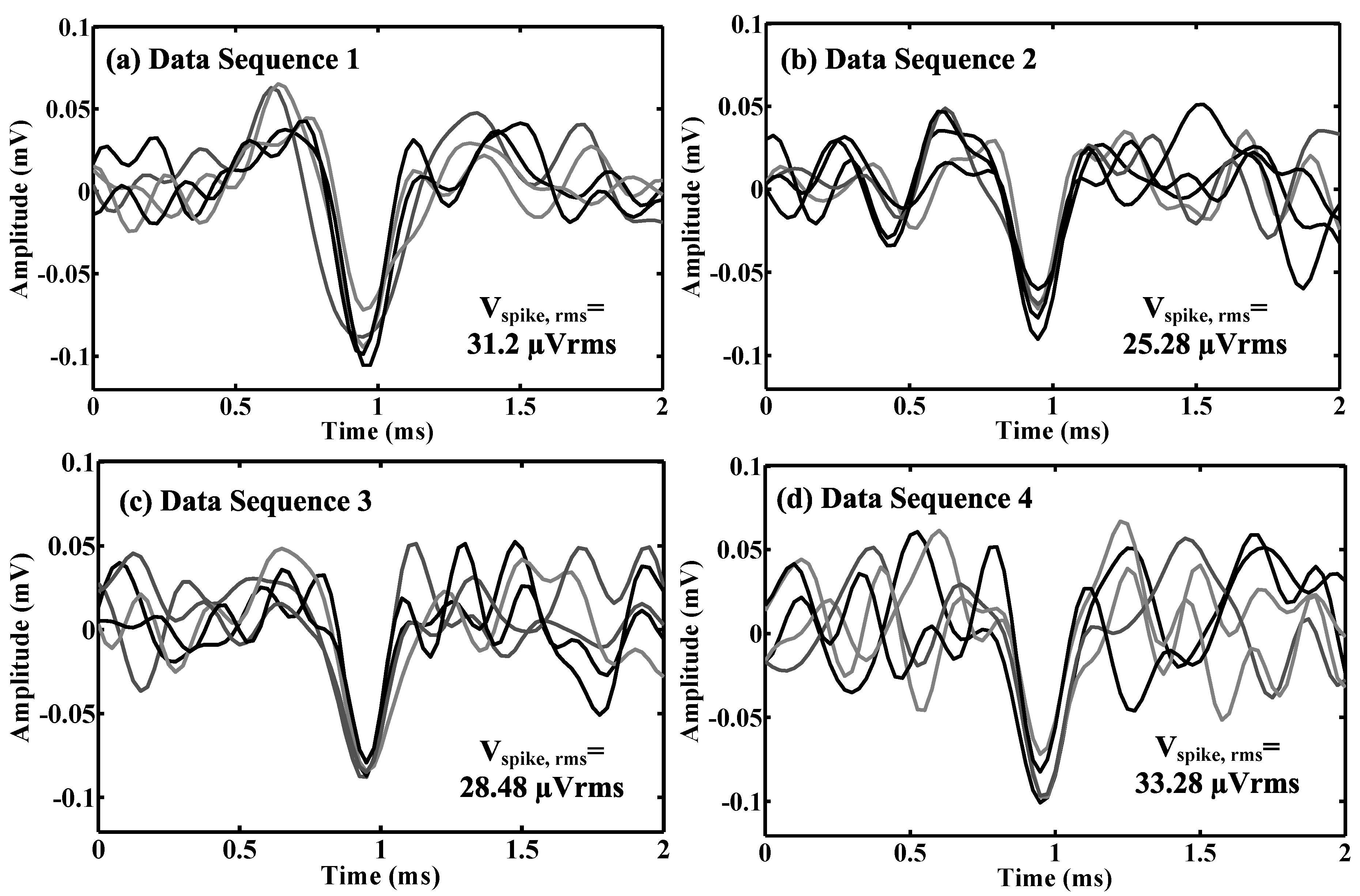
2. In Vivo Neural Data Dynamic Range Analysis
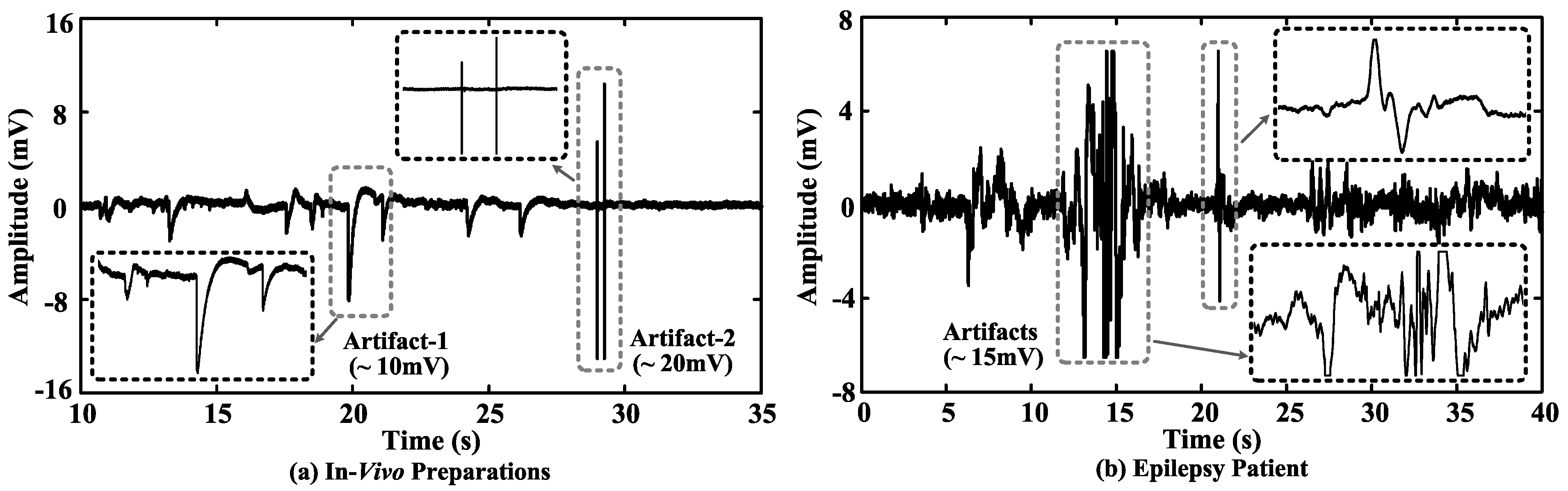

| Parameter | In Vivo Neural Data (1 Hz–10 kHz) | Epilepsy Patient Data (0.5 Hz–9 kHz) |
|---|---|---|
| Dynamic range without artifacts | (10.57 ± 0.32)-bit | (9.55 ± 0.31)-bit |
| Dynamic range with artifacts | (12.82 ± 0.76)-bit | (12.41 ± 0.68)-bit |
| Increase in dynamic range | 2.25-bit | 2.86-bit |

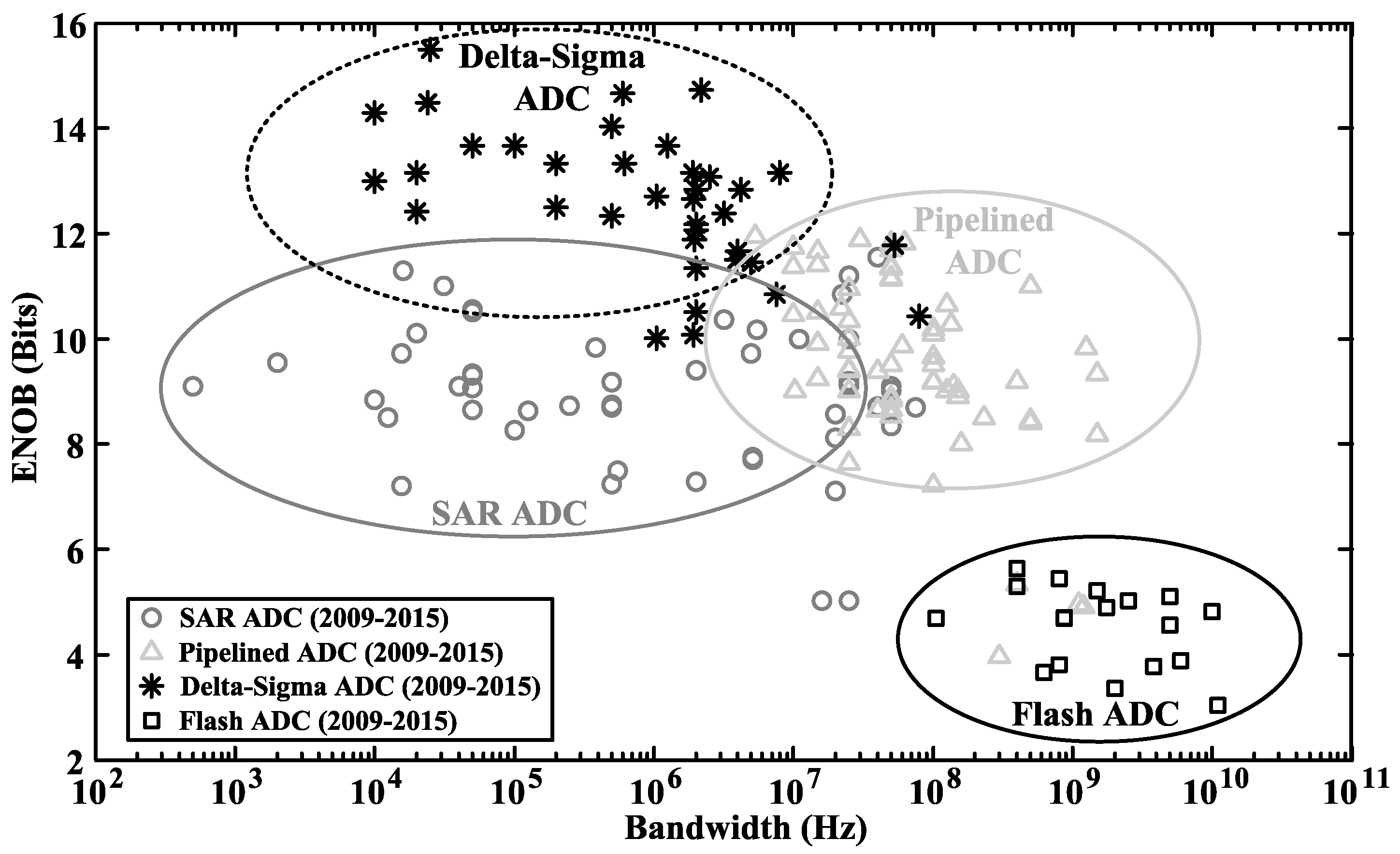
3. ADC Architecture Comparison and Selection

4. Multi-Bit Switched Op-Amp-Based Delta-Sigma Modulator Design
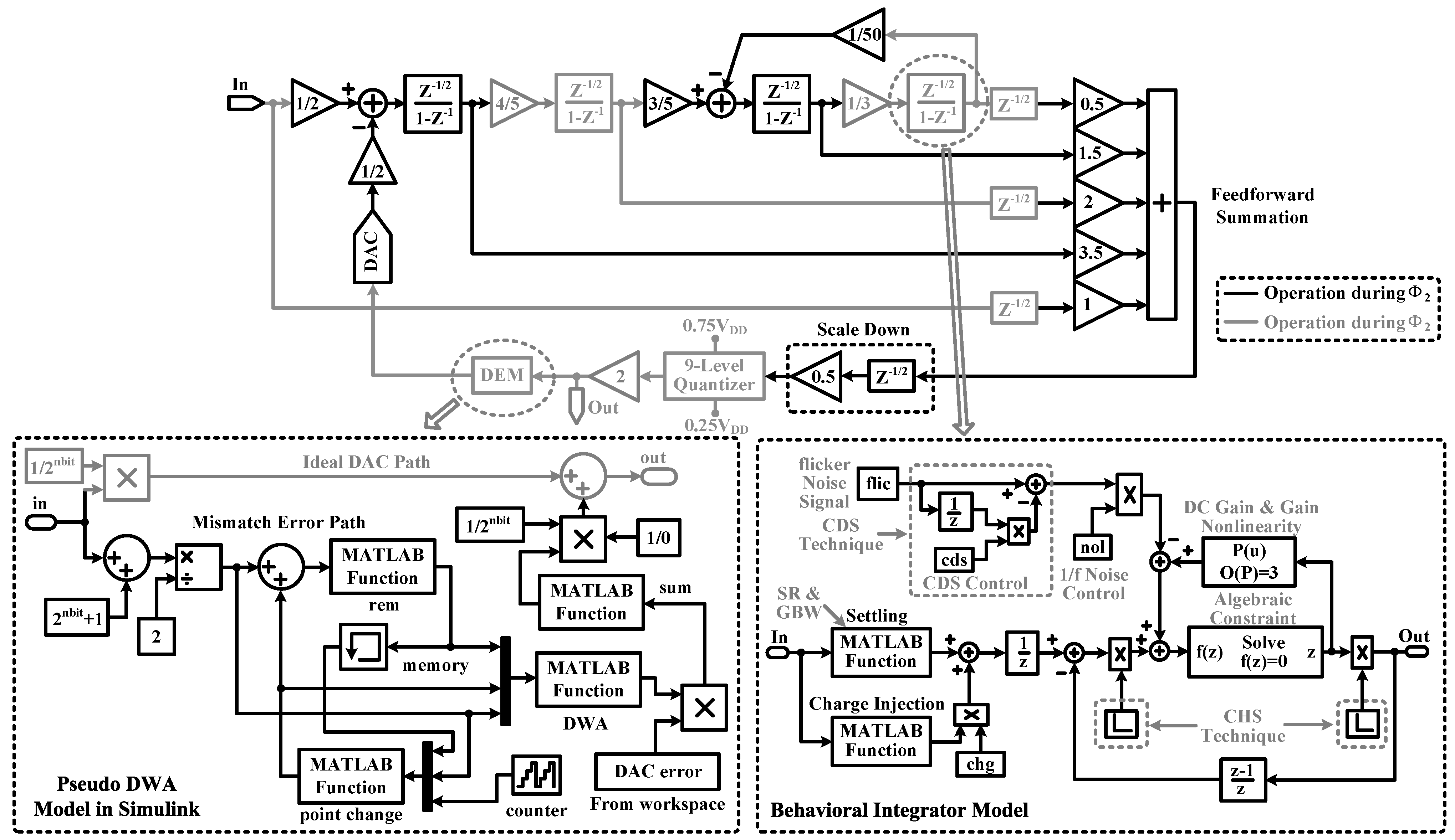
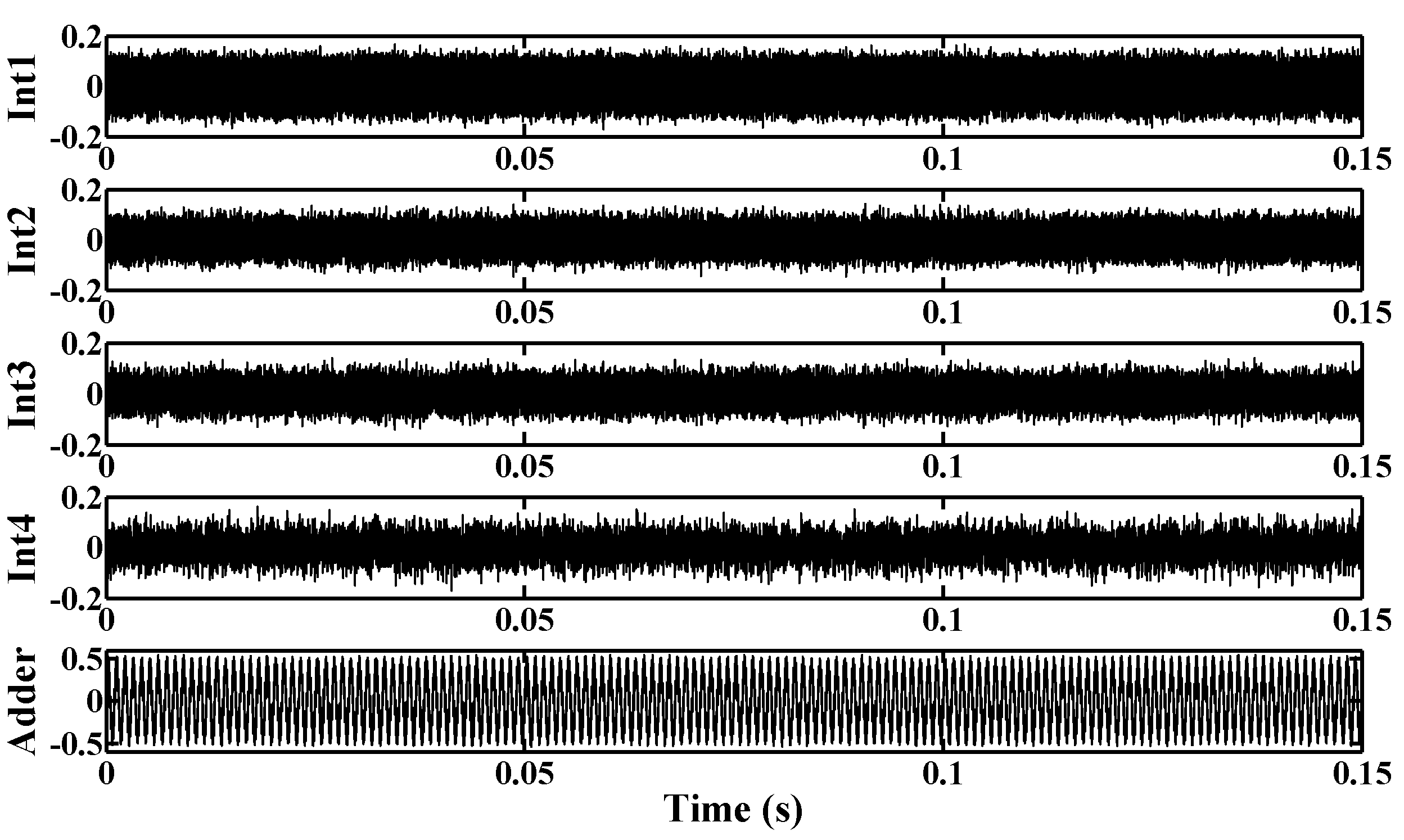
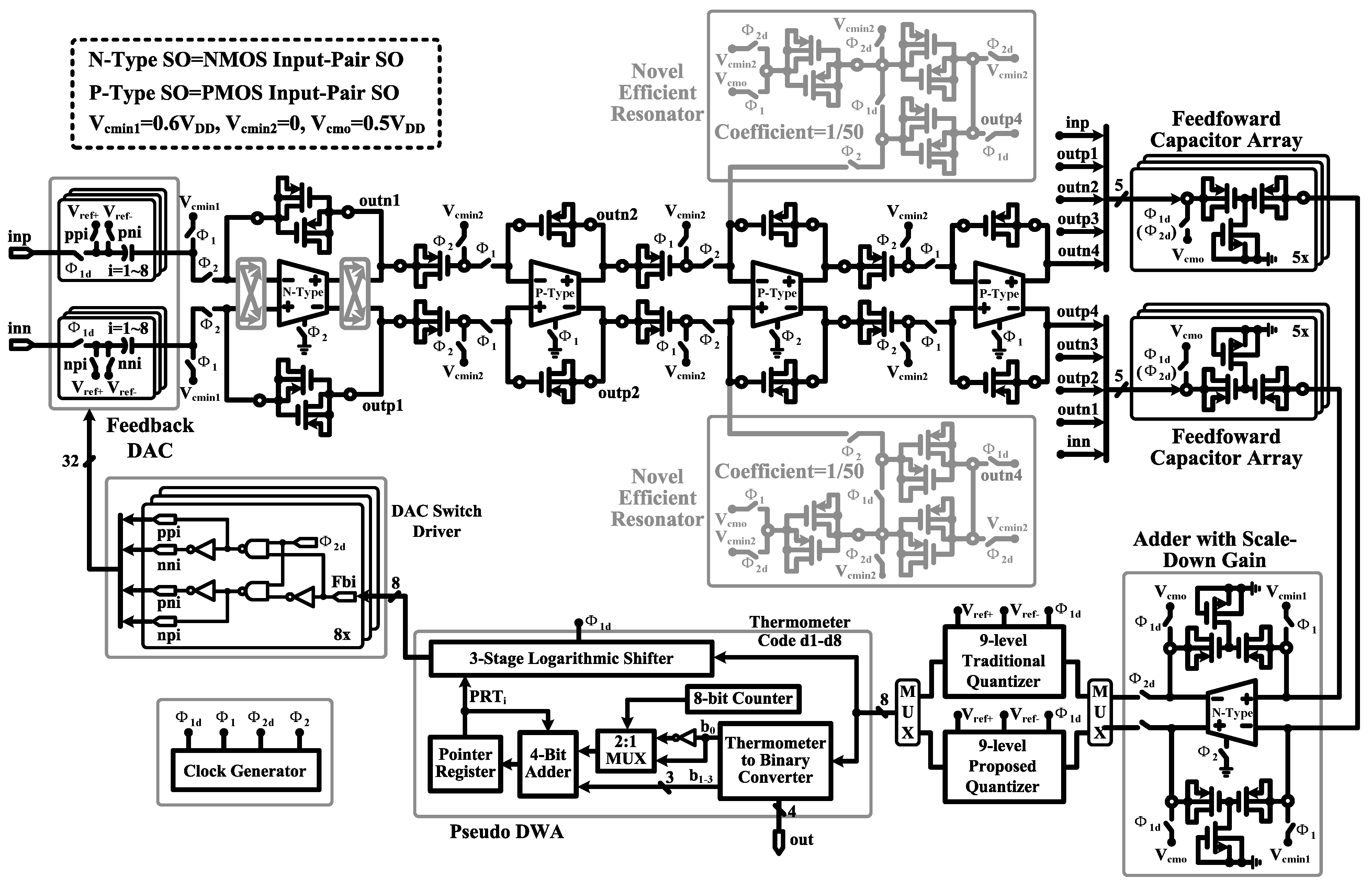
4.1. Delta-Sigma Modulator Topology

4.2. Design Analysis on Non-Ideal Factors
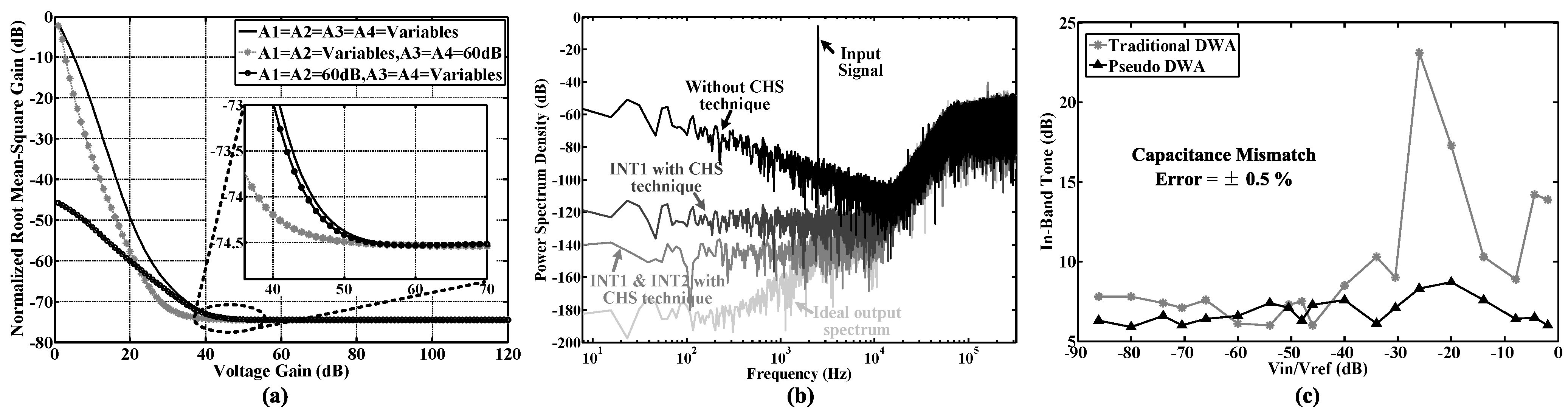
4.2.1. Finite Amplifier Gain

4.2.2. Chopper Stabilization
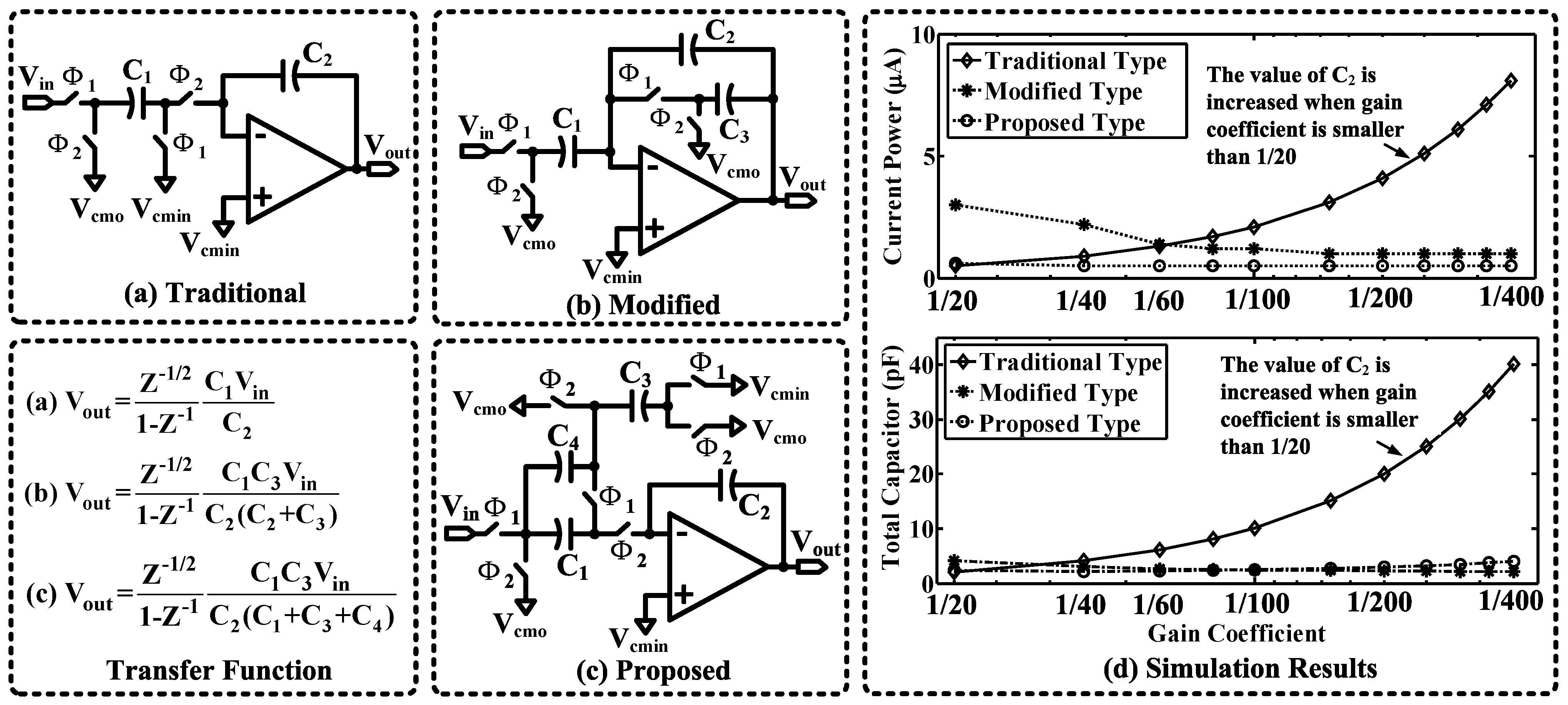
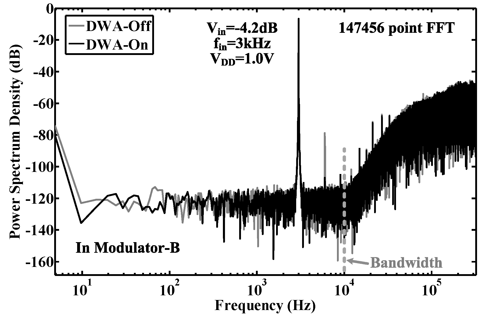
4.2.3. Pseudo Data Weighted Averaging
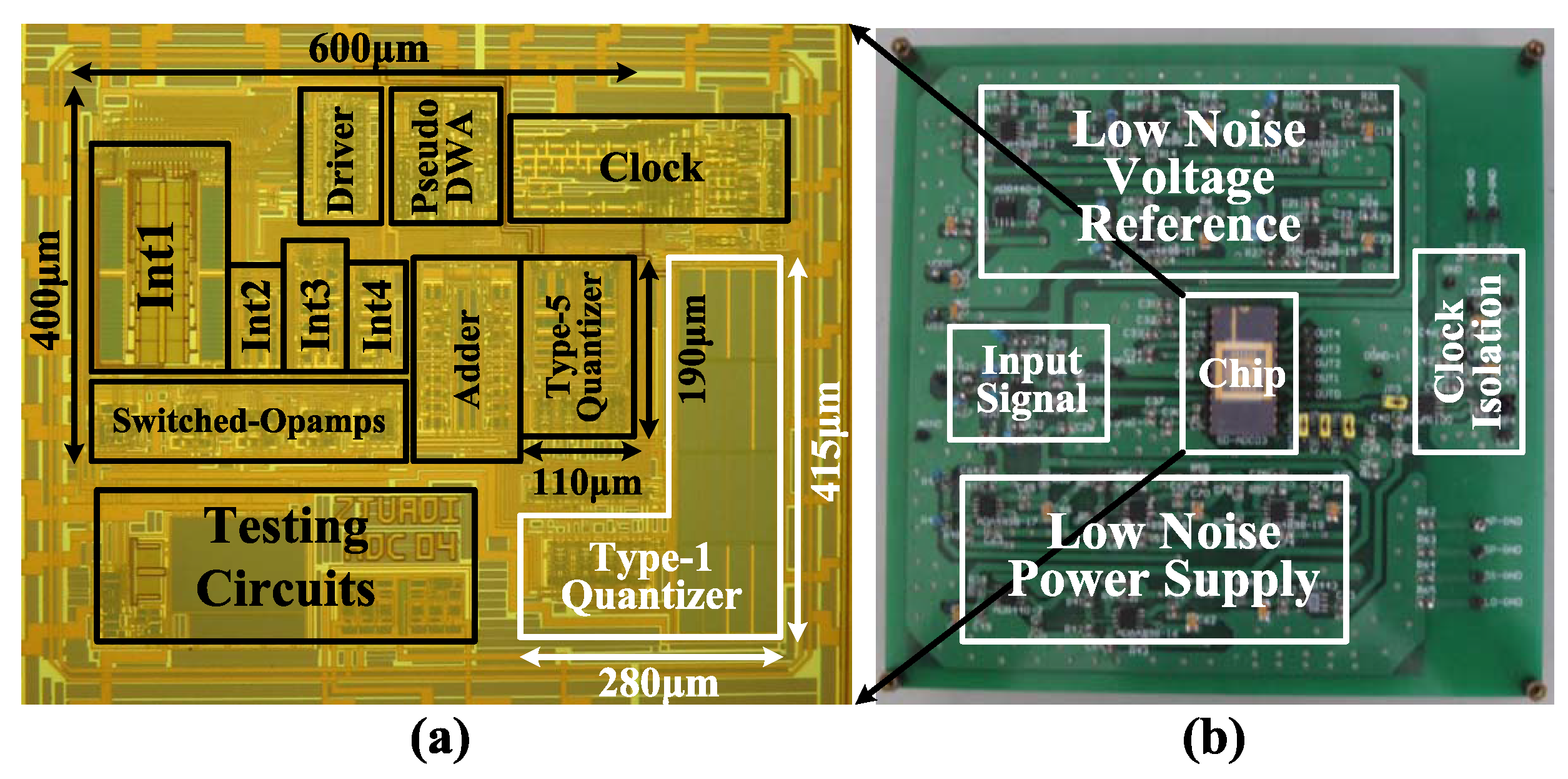
5. Circuit Design and Implementation
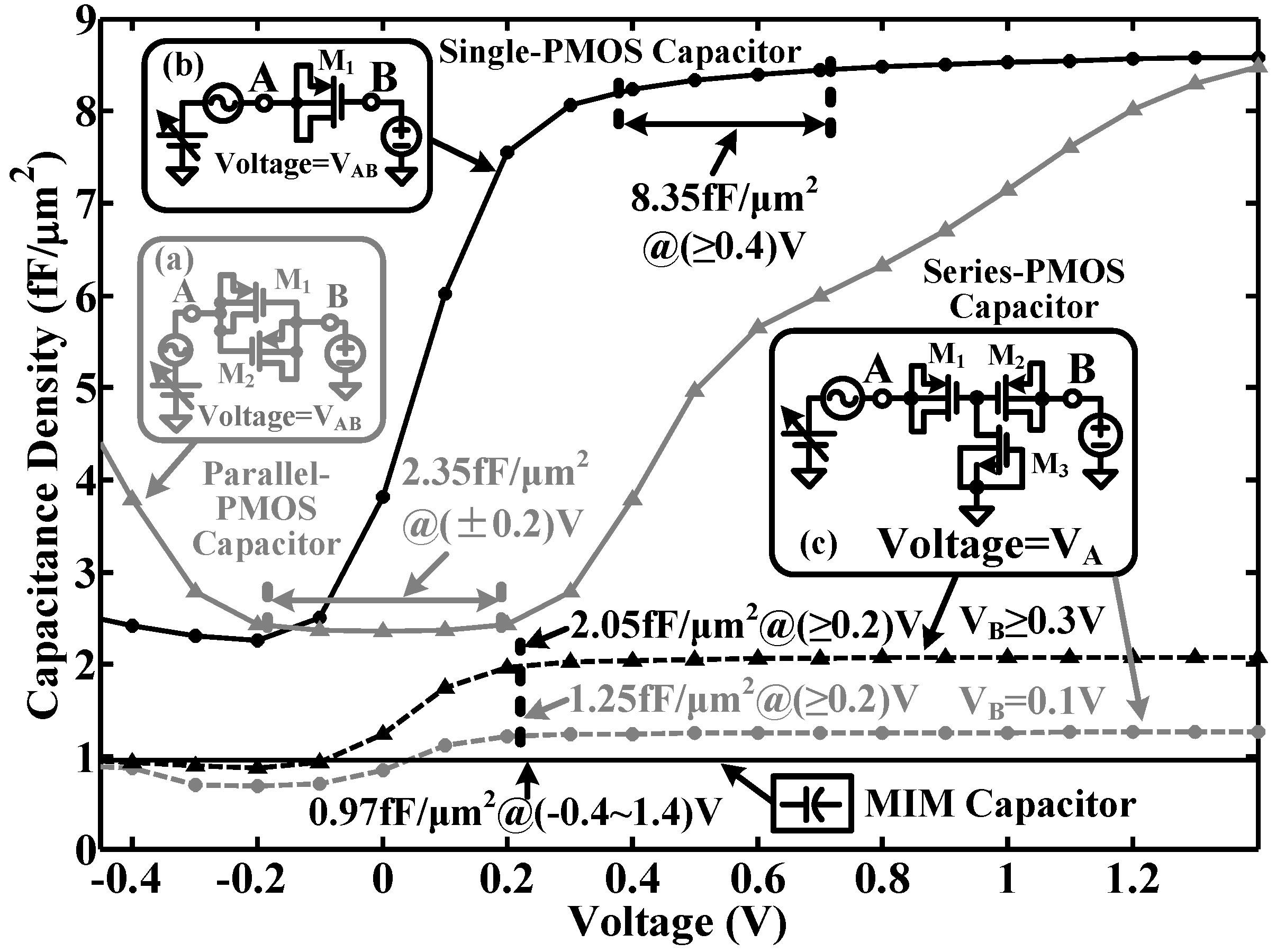
5.1. High Density MOS Capacitors


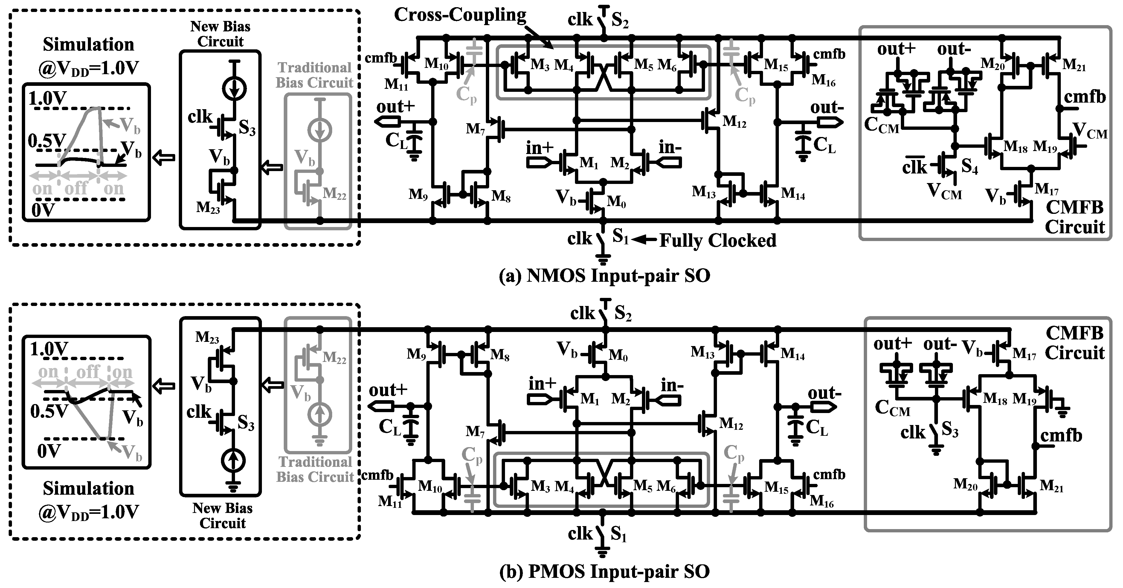
5.2. Fully-Clocked Power-Efficient Switched Op-Amp

| Parameter | NMOS Input-Pair Switched Op-Amp | PMOS Input-Pair Switched Op-Amp |
|---|---|---|
| Gain A | 61.1 dB | 57.7 dB |
| Phase Margin | 58.0∘ | 50.8∘ |
| 5.1 MHz | 4.9 MHz | |
| 4 pF | 4 pF | |
| Current Power | 3.0 μA at 1.0 V | 3.4 μA at 1.0 V |
| Noise Power | 17.8 μV at (1–10 k) Hz | 70.8 μV at (1–10 k) Hz |
| 5.0 μV at (150 k–160 k) Hz | 15.8 μV at (150 k–160 k) Hz | |
| FOM | 6800 MHz·pF/mA | 5765 MHz·pF/mA |
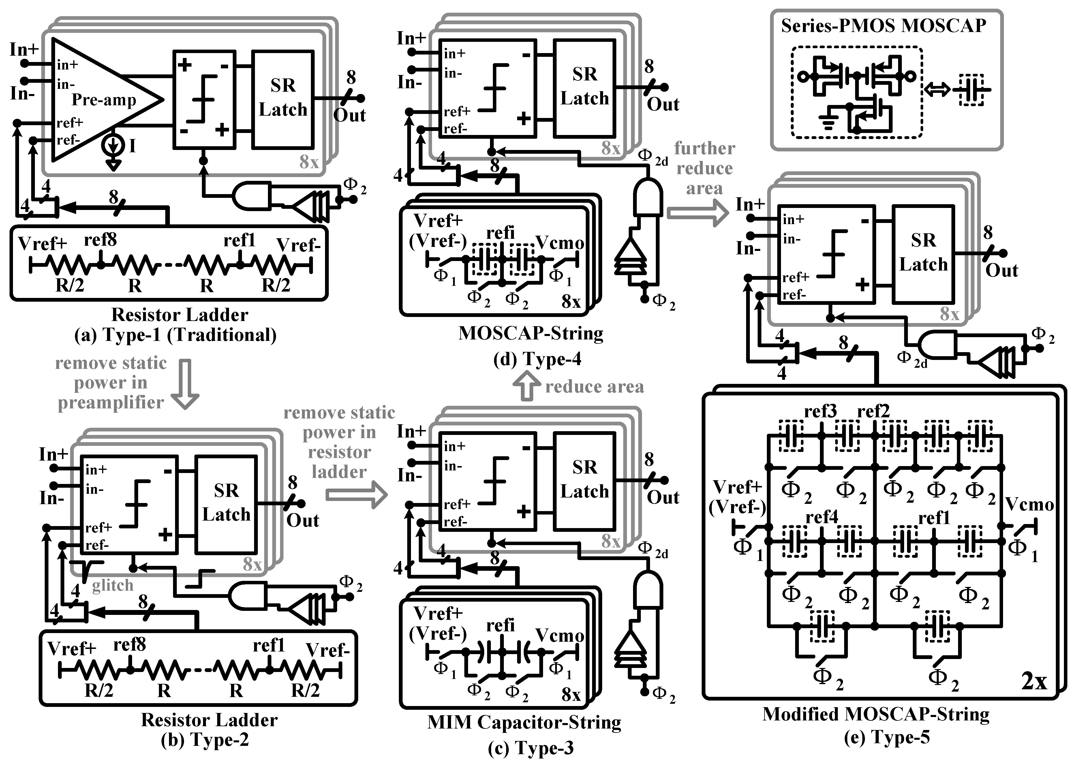
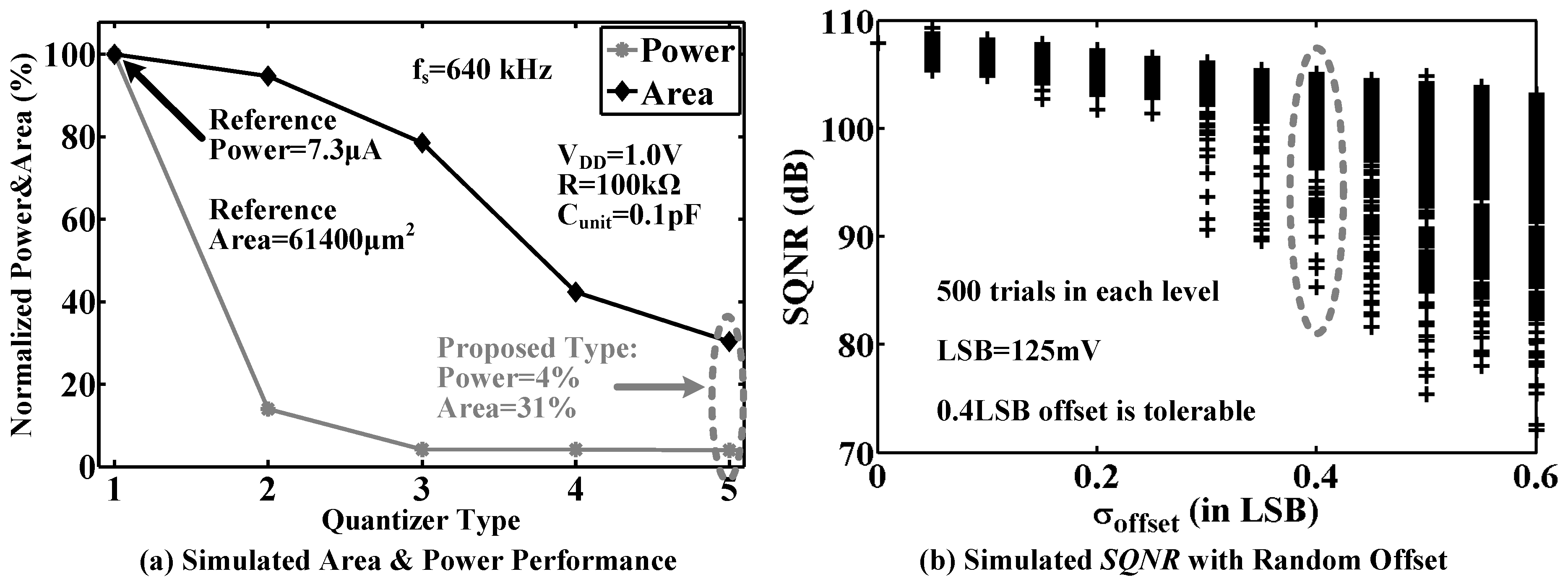
5.3. Static Power-Less Area-Efficient Quantizer
5.4. Novel Power- and Area-Efficient Resonator


5.5. Complete Modulator Circuit
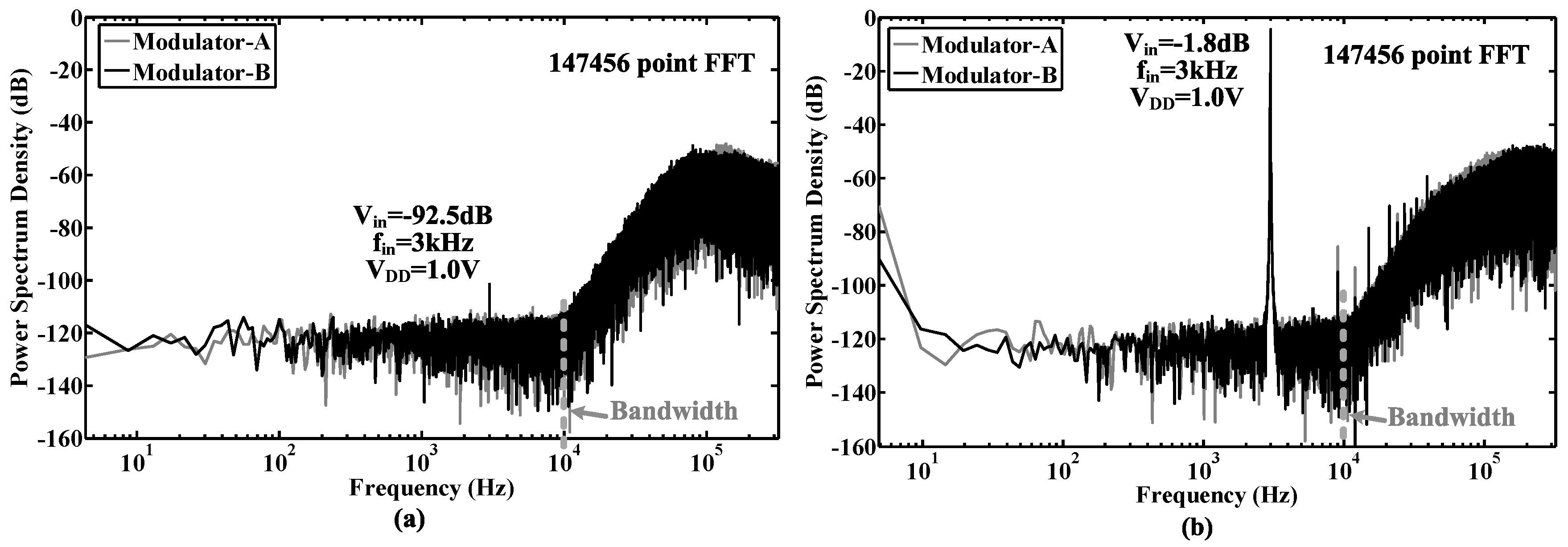
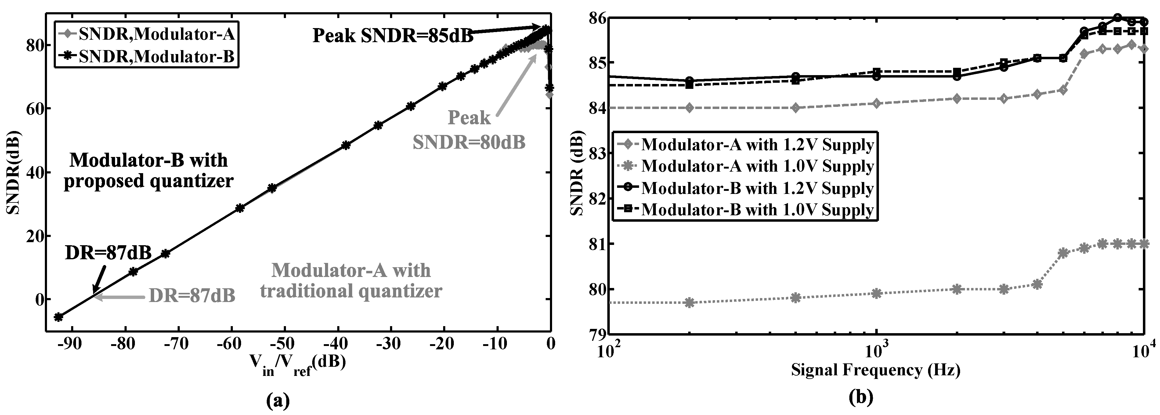
6. Measurement Results


| Modulator | [49] | [50] | [26] | [30] | [51] | [28] | [25] | This Work |
|---|---|---|---|---|---|---|---|---|
| Process (nm) | 130 | 65 | 180 | 180 | 180 | 180 | 180 | 180 |
| Integrator Type | Inverter | Comp. | SO | OTA | OTA | OTA | Inverter | SO |
| (V) | 1.2 | 1.2 | 0.7 | 0.7 | 1.8 | 1.0 | 0.7 | 1.0 |
| (MHz) | 1.28 | 40 | 5 | 1.024 | 6.144 | 4 | 4 | 0.64 |
| Bandwidth (kHz) | 20 | 2500 | 25 | 8 | 24 | 20 | 20 | 10 |
| Power (μW) | 165 | 3730 | 870 | 80 | 110 | 140 | 36 | 13 |
| Dynamic Range (dB) | 83.0 | 71.3 | 100 | 75 | 92.5 | 88 | 85 | 87 |
| SNDR (dB) | 72.5 | 70.4 | 95 | 67 | 88 | 81 | 81 | 85 |
| FOM (fJ/conversion step) | 1197 | 276 | 378.5 | 2733 | 111.6 | 381.7 | 98.1 | 45 |
7. Conclusions
Acknowledgments
Author Contributions
Conflicts of Interest
References
- Lee, S.; Lee, H.; Kiani, M.; Jow, U.; Ghovanloo, M. An inductively powered scalable 32-channel wireless neural recording system-on-a-chip for neuroscience applications. IEEE Trans. Biomed. Circuits Syst. 2010, 4, 360–371. [Google Scholar]
- Muller, R.; Gambini, S.; Rabaey, J. A 0.013 mm2, 5 μW, DC-coupled neural signal acquisition IC with 0.5 V supply. IEEE J. Solid-State Circuits 2012, 47, 232–243. [Google Scholar]
- Stevenson, I.; Kording, K. How advances in neural recording affect data analysis. Nat. Neurosci. 2011, 14, 139–142. [Google Scholar] [CrossRef] [PubMed]
- Teo, T.; Qian, X.; Kumar, G.; Hwan, Y.; Haridas, K.; Pang, C.; Cha, H.; Je, M. A 700-μW wireless sensor node SoC for continuous real-time health monitoring. IEEE J. Solid-State Circuits 2010, 45, 2292–2299. [Google Scholar]
- Gao, H.; Walker, R.; Nuyujukian, P.; Makinwa, K.; Shenoy, K.; Murmannn, B.; Meng, T. HermesE: A 96-channel full data rate direct neural interface in 0.13 μm CMOS. IEEE J. Solid-State Circuits 2012, 47, 1043–1055. [Google Scholar] [CrossRef]
- Zhang, F.; Holleman, J.; Otis, B. Design of ultra-low power biopotential amplifiers for biosignal acquisition applications. IEEE Trans. Biomed. Circuits Syst. 2012, 6, 344–355. [Google Scholar] [CrossRef] [PubMed]
- Guo, J.; Yuan, J.; Huang, J.; Law, J.; Yeung, C.; Chan, M. 32.9 nV/rt Hz—60.6 dB THD dual-band micro-electrode array signal acquisition IC. IEEE J. Solid-State Circuits 2012, 47, 1209–1220. [Google Scholar]
- Zou, X.; Xu, X.; Yao, L.; Lian, Y. A 1-V 450-nW fully integrated programmable biomedical sensor interface chip. IEEE J. Solid-State Circuits 2009, 44, 1067–1077. [Google Scholar] [CrossRef]
- Park, H.; Kiani, M.; Lee, H.; Kim, J.; Gosselin, B.; Ghovanloo, M. A wireless magnetoresistive sensing system for an intraoral tongue-computer interface. IEEE Trans. Biomed. Circuits Syst. 2012, 6, 571–585. [Google Scholar] [CrossRef] [PubMed]
- Shahrokhi, F.; Abdelhalim, K.; Serletis, S.; Carlen, P.; Genov, R. The 128-channel fully differential digital integrated neural recording and stimulation interface. IEEE Trans. Biomed. Circuits Syst. 2010, 4, 149–161. [Google Scholar] [CrossRef] [PubMed]
- Salam, M.; Sawan, M.; Dang, K.N. A novel low-power-implantable epileptic seizure-onset detector. IEEE Trans. Biomed. Circuits Syst. 2011, 5, 568–578. [Google Scholar] [CrossRef] [PubMed]
- Rieger, R.; Taylor, J. A switched-capacitor front-end for velocity-selective eng recording. IEEE Trans. Biomed. Circuits Syst. 2013, 7, 480–488. [Google Scholar] [CrossRef] [PubMed]
- Roham, M.; Covey, D.; Daberkow, D.; Ramsson, E.; Howard, C.; Heidenreich, B.; Garris, P.; Mohseni, P. A wireless IC for time-share chemical and electrical neural recording. IEEE J. Solid-State Circuits 2009, 44, 3645–3658. [Google Scholar] [CrossRef]
- Rieger, R.; Deng, S. Double-differential recording and AGC using microcontrolled variable gain ASIC. IEEE Trans. Neural Syst. Rehabil. Eng. 2013, 21, 47–54. [Google Scholar] [CrossRef] [PubMed]
- Lapolli, A.; Coppa, B.; Heliot, R. Low-power hardware for neural spike compression in BMIs. In Proceedings of the 35th Annual International Conference of the IEEE Engineering in Medicine and Biology Socirty, Osaka, Japan, 3–7 July 2013; pp. 2156–2159.
- Huang, W.; Hung, S.; Chung, J.; Chang, M.; Van, L.; Lin, C.T. FPGA implementation of 4-channel ICA for on-line EEG signal separation. In Proceedings of the IEEE Biomedical Circuits and Systems Conference, Baltimore, MD, USA, 20–22 November 2008; pp. 65–68.
- Clements, M.; Vichienchom, K.; Liu, W.; Hughes, C.; McGucken, E.; DeMarco, C.; Mueller, J.; Humayun, M.; de Juan, E.; Weiland, J.; et al. An implantable neuro-stimulator device for a retinal prosthesis. In Proceedings of the IEEE International Solid-State Circuits Conference, San Francisco, CA, USA, 17 February 1999; pp. 216–217.
- Mollazadeh, M.; Murari, K.; Cauwenberghs, G.; Thakor, N. Micropower CMOS integrated low-noise amplification, filtering, and digitization of multimodal neuropotentials. IEEE Trans. Biomed. Circuits Syst. 2009, 3, 1–10. [Google Scholar] [CrossRef] [PubMed]
- Gosselin, B. Recent advances in neural recording microsystems. Sensors 2011, 11, 4572–4597. [Google Scholar] [CrossRef] [PubMed]
- Qian, C.; Shi, J.; Parramon, J.; Sanchez-Sinencio, E. A low-power configurable neural recording system for epileptic seizure detection. IEEE Trans. Biomed. Circuits Syst. 2013, 7, 499–512. [Google Scholar] [CrossRef] [PubMed]
- Brown, E.; Ross, J.; Blum, R.; Nam, Y.; Wheeler, B.; DeWeerth, S. Stimulus-artifact elimination in a multi-electrode system. IEEE Trans. Biomed. Circuits Syst. 2008, 2, 10–21. [Google Scholar] [CrossRef] [PubMed]
- Van, H.; Kim, S.; Kim, H.; Kim, J.; Van, H.C.; Yazicioglu, R. A 160 μA biopotential acquisition IC with fully integrated IA and motion artifact suppression. IEEE Trans. Biomed. Circuits Syst. 2012, 6, 552–561. [Google Scholar]
- Gnadt, J.; Echols, S.; Yildirim, A.; Zhang, H.; Paul, K. Spectral cancellation of microstimulation artifact for simultaneous neural recording in situ. IEEE Trans. Biomed. Eng. 2003, 50, 1129–1135. [Google Scholar] [CrossRef] [PubMed]
- Wang, L.; Theogarajan, L. A micro power delta-sigma modulator based on a self-biased super inverter for neural recording systems. In Porceedings of the IEEE Custom Integrated Circuits Conference, San Jose, CA, USA, 19–22 September 2010; pp. 1–4.
- Chae, Y.; Lee, I.; Han, G. A 0.7 V 36 μW 85 dB-DR audio ΣΔ modulator using class-c inverter. In Porceedings of the IEEE International Solid-State Circuits Conference, San Francisco, CA, USA, 3–7 February 2008; pp. 490–491.
- Park, H.; Nam, K.; Su, D.; Vleugels, K.; Wooley, B. A 0.7-V 100-dB 870-μW digital audio ΣΔ modulator. In Porceedings of the IEEE Symposium on VLSI Circuits, Honolulu, HI, USA, 18–20 June 2008; pp. 178–179.
- Goes, J.; Vaz, B.; Monteiro, R.; Paulino, N. A 0.9 V ΔΣ modulator with 80 dB SNDR and 83 dB DR using a single-phase technique. In Porceedings of the IEEE International Solid-State Circuits Conference, San Francisco, CA, USA, 6–9 February 2006; pp. 191–200.
- Yao, L.; Steyaert, M.; Sansen, W. A 1-V 140-μW 88-dB audio sigma-delta modulator in 90-nm CMOS. IEEE J. Solid-State Circuits 2004, 39, 1809–1818. [Google Scholar]
- Wang, L.; Theogarajan, L. An 18 μW 79 dB-DR 20 KHz-BW MASH sigma-delta modulator utilizing self-biased amplifiers for biomedical applications. In Porceedings of the IEEE Custom Integrated Circuits Conference, San Jose, CA, USA, 19–21 September 2011; pp. 1–4.
- Sauerbrey, J.; Tille, T.; Schmitt-Landsiedel, D.; Thewes, R. A 0.7-V MOSFET-only switched-op-amp ΣΔ modulator in standard digital CMOS technology. IEEE J. Solid-State Circuits 2002, 37, 1662–1669. [Google Scholar]
- Xu, J.; Wu, X.; Zhao, M.; Fan, R.; Wang, H.; Ma, X.; Liu, B. Ultra low-FOM high-precision ΔΣ modulators with fully-clocked SO and zero static power quantizers. In Porceedings of the IEEE Custom Integrated Circuits Conference, San Jose, CA, USA, 19–21 September 2011; pp. 1–4.
- Buzsaki, G.; Anastassiou, C.; Koch, C. The origin of extracellular fields and currents-EEG, ECoG, LFP and spikes. Nat. Rev. Neuronsci. 2012, 13, 407–420. [Google Scholar] [CrossRef] [PubMed]
- Murmann, B. ADC Performance Survey 1997–2015. Available online: http://web.stanford.edu/murmann/adcsurvey.html (accessed on 14 June 2015).
- Wattanapanitch, R.; Sarpeshkar, R. A low-power 32-channel digitally programmable neural recording integrated circuit. IEEE Trans. Biomed. Circuits Syst. 2011, 5, 592–601. [Google Scholar] [CrossRef] [PubMed]
- Lopez, C.; Prodanov, D.; Braeken, D.; Gligorijevic, I.; Eberle, W.; Bartic, C.; Puers, R.; Gielen, G. A multichannel integrated circuit for electrical recording of neural activity, with independent channel programmability. IEEE Trans. Biomed. Circuits Syst. 2012, 6, 101–110. [Google Scholar] [CrossRef] [PubMed]
- Zhou, X.; Liew, W.; Yao, L.; Lian, Y. A 1 V 22 μW 32-channel implantable EEG recording IC. In Proceedings of the IEEE International Solid-State Circuits Conference, San Francisco, CA, USA, 7–11 February 2010; pp. 122–123.
- Gosselin, B.; Ayoub, A.; Roy, J.; Sawan, M.; Lepore, F.; Chaudhuri, A.; Guitton, D. A mixed-signal multichip neural recording interface with bandwidth reduction. IEEE Trans. Biomed. Circuits Syst. 2009, 3, 129–141. [Google Scholar] [CrossRef] [PubMed]
- Alberto, R.; Jesus, R.; Manuel, D.; Angel, R. A low-power programmable neural spike detection channel with embedded calibration and data compression. IEEE Trans. Biomed. Circuits Syst. 2012, 6, 87–100. [Google Scholar]
- Bonfanti, A.; Ceravolo, M.; Zambra, G.; Gusmeroli, R.; Borghi, T.; Spinelli, A.; Lacaita, A. A 0.7-V 100-dB 870-μW digital audio ΣΔ modulator. In Proceedings of the IEEE European Solid-State Circuits Conference (ESSCIRC), Seville, Spain, 14–16 September 2010; pp. 330–333.
- Lo, Y.; Liu, W.; Chen, K.; Tsai, M.; Hsueh, F. A 64-channel neuron recording system. In Proceedings of the 33th Annual International Conferenceof the IEEE Engineering in Medicine and Biology Society, Boston, MA, USA, 30 August–3 September 2011; pp. 2862–2865.
- Do, A.; Tan, Y.; Lam, C.; Je, M.; Yeo, K. Low power implantable neural recording front-end. In Proceedings of the IEEE International SoC Design Conference (ISOCC), Jeju Island, Korea, 4–7 November 2012; pp. 387–390.
- Hamoui, A.; Martin, K. High-order multibit modulators and pseudo data-weighted-averaging in low-oversampling ΔΣ ADCs for broad-band applications. IEEE Trans. Circuits Syst. I 2004, 51, 72–85. [Google Scholar] [CrossRef]
- Xu, J.; Wu, X.; Zhao, M.; Shen, J. A 20 μW 95 dB dynamic range 4th-order Delta-Sigma modulator with novel power efficient operational transconductance amplifier and resonator. J. Zhejiang Univ. Sci. C 2011, 12, 486–498. [Google Scholar] [CrossRef]
- Ma, X.; Xu, J.; Wu, X. Dual cycle shift data-weighted averaging technique for multi-bit sigma-delta modulators. In Proceedings of the IEEE International Electron Devices and Solid-State Circuits Conference (EDSSC), Xi’an, China, 25–27 December 2009; pp. 174–177.
- Denison, T.; Consoer, K.; Kelly, A.; Hachenburg, A.; Santa, W. A 2.2 μW 94 , chopper-stabilized instrumentation amplifier for EEG detection in chronic implants. In Proceedings of the IEEE International Solid-State Circuits Conference, San Francisco, CA, USA, 11–15 February 2007; pp. 162–163.
- Chen, H.; Chen, P.; Chiang, J. A low-offset low-noise sigma-delta modulator with pseudorandom chopper-stabilization technique. IEEE Trans. Circuits Syst. I 2009, 56, 2533–2543. [Google Scholar] [CrossRef]
- Enz, C.; Temes, G. Circuit techniques for reducing the effects of op-amp imperfections: Autozeroing, correlated double sampling, and chopper stabilization. IEEE Proc. 1996, 84, 1584–1614. [Google Scholar] [CrossRef]
- Nagaraj, K. A parasitic-insensitive area-efficient approach to realizing very large time constants in switched-capacitor circuits. IEEE Trans. Circuits Syst. I 1989, 36, 1210–1216. [Google Scholar] [CrossRef]
- Custodio, J.; Goes, J.; Paulino, N.; Oliveira, J.; Bruun, E. A 1.2-V 165-μW 0.29-mm2 multibit Sigma-Delta ADC for hearing aids using nonlinear DACs and with over 91 dB dynamic-range. IEEE Trans. Biomed. Circuits Syst. 2013, 7, 376–385. [Google Scholar]
- Yamamoto, K.; Carusone, A. A 1-1-1-1 MASH Delta-Sigma modulator with dynamic comparator-based OTAs. IEEE J. Solid-State Circuits 2012, 47, 1866–1883. [Google Scholar] [CrossRef]
- Pavan, S.; Sankar, P. An 110 μW single bit audio continuous-time oversampled converter with 92.5 dB dynamic range. In Proceedings of the IEEE European Solid-State Circuits Conference (ESSCIRC), Athens, Greece, 14–18 September 2009; pp. 320–323.
© 2015 by the authors; licensee MDPI, Basel, Switzerland. This article is an open access article distributed under the terms and conditions of the Creative Commons Attribution license (http://creativecommons.org/licenses/by/4.0/).
Share and Cite
Xu, J.; Zhao, M.; Wu, X.; Islam, M.K.; Yang, Z. A High Performance Delta-Sigma Modulator for Neurosensing. Sensors 2015, 15, 19466-19486. https://doi.org/10.3390/s150819466
Xu J, Zhao M, Wu X, Islam MK, Yang Z. A High Performance Delta-Sigma Modulator for Neurosensing. Sensors. 2015; 15(8):19466-19486. https://doi.org/10.3390/s150819466
Chicago/Turabian StyleXu, Jian, Menglian Zhao, Xiaobo Wu, Md. Kafiul Islam, and Zhi Yang. 2015. "A High Performance Delta-Sigma Modulator for Neurosensing" Sensors 15, no. 8: 19466-19486. https://doi.org/10.3390/s150819466
APA StyleXu, J., Zhao, M., Wu, X., Islam, M. K., & Yang, Z. (2015). A High Performance Delta-Sigma Modulator for Neurosensing. Sensors, 15(8), 19466-19486. https://doi.org/10.3390/s150819466