An Improved Equivalent Simulation Model for CMOS Integrated Hall Plates

Abstract
: An improved equivalent simulation model for a CMOS-integrated Hall plate is described in this paper. Compared with existing models, this model covers voltage dependent non-linear effects, geometrical effects, temperature effects and packaging stress influences, and only includes a small number of physical and technological parameters. In addition, the structure of this model is relatively simple, consisting of a passive network with eight non-linear resistances, four current-controlled voltage sources and four parasitic capacitances. The model has been written in Verilog-A hardware description language and it performed successfully in a Cadence Spectre simulator. The model’s simulation results are in good agreement with the classic experimental results reported in the literature.1. Introduction
Presently, CMOS integrated Hall magnetic sensors are widely used in many practical fields. Besides directly measuring the value of magnetic field, they are usually used to indirectly measure position, distance, speed, rotational angle or an electric current [1,2]. For instance, they can act as an automotive vehicle speed sensor, a replacement for mechanical switches, a brushless control for DC motors, and so on. Unfortunately, CMOS integrated Hall sensors have traditionally suffered from a lot of non-idealities, such as low sensitivity, large offset, temperature drifts, non-linearity and packaging stress influence etc., which severely deteriorates their performance [3]. As a consequence, CMOS integrated Hall devices must depend on the processing circuit for offset and noise cancellation, temperature compensation and non-linearity correction. In order to facilitate the simulation analysis of electrical circuit with integrated Hall devices, it is necessary to extract a precise simulation model to take into account important physical effects and technological influences. Furthermore, the extracted model should be simple and conveniently implemented in standard SPICE-like EDA tools.
Several compact simulation models of Hall elements have been put forward. Previously reported 4-resistance Wheatstone bridge models don’t fully take into account correlative physical and geometrical effects such as non-linear conductivity, junction effect, temperature drift, frequency-response, noise behavior and device shape-dependent sensitivity [4,5]. Later, Dimitropoulos et al. proposed a completely scalable lumped-circuit model to analyze all those effects, except for the influence of packaging stress [6]. The basic component for the lumped-circuit model consists of JFETs and current-controlled current sources. The number of these components can be freely increased to achieve the required accuracy at the expense of computation efficiency. However, this macro model needs an accurate JEFTs device model which normally cannot be provided by the standard CMOS technology. Recently, Madec et al. developed a compact model of a cross-shaped horizontal integrated Hall sensor [7]. It uses six sub-components to accurately model the non-linear resistance, allowing for the influence of space charge region modulation due to sensor bias. Unfortunately, it cannot consider sensitivity drifts, temperature drifts and influence of mechanical stress on offset. Besides, the resistance computation of the model has to be fed by empirical parameters through FEM (finite element method) simulation.
In this paper, an accurate 8-resistance simulation model for a cross-shaped CMOS-integrated Hall plate is developed. To be conveniently used by circuit designers, this model is improved by replacing the JFETs with passive non-linear resistances and depletion capacitances. It takes into account voltage dependent non-linear effects, geometrical effects, temperature effects, and packaging stress influence, etc. Since we mainly deal with the magnetic sensors operating in a weak magnetic field in this work, two additional strong magnetic field related effects, namely magneto-resistance and carriers scattering, are not included in this model. The model has been written in Verilog-A hardware description language and was successfully tested in a Cadence Spectre simulator. This paper is organized as follows: in Section 2, we introduce the structure of the model and analyze the important physical effects of the Hall device with the basic equations. Furthermore, the detailed computation of device parameters in this model is presented. In Section 3, the simulation results of the model are compared with the classic experimental results reported in the literature. Section 4 summarizes this paper with some ideas for future work.
2. The Improved Compact Model
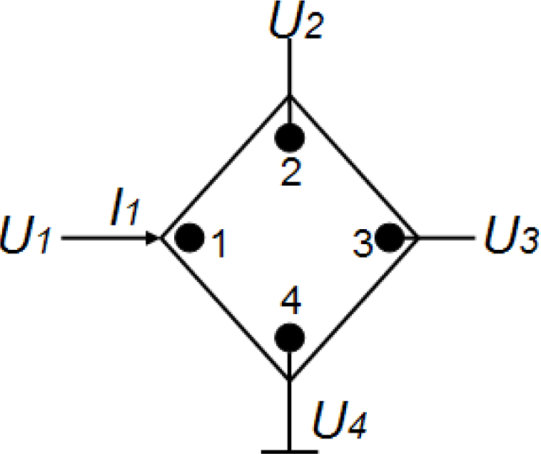
To be compatible with the spinning current techniques for reducing Hall offset [3], 90° symmetry Hall plates with square or cross-shaped structures are usually recommended. We can obtain the Z-matrix for the 90° symmetry Hall plates with four contacts illustrated in Figure 1 as follows [8]:
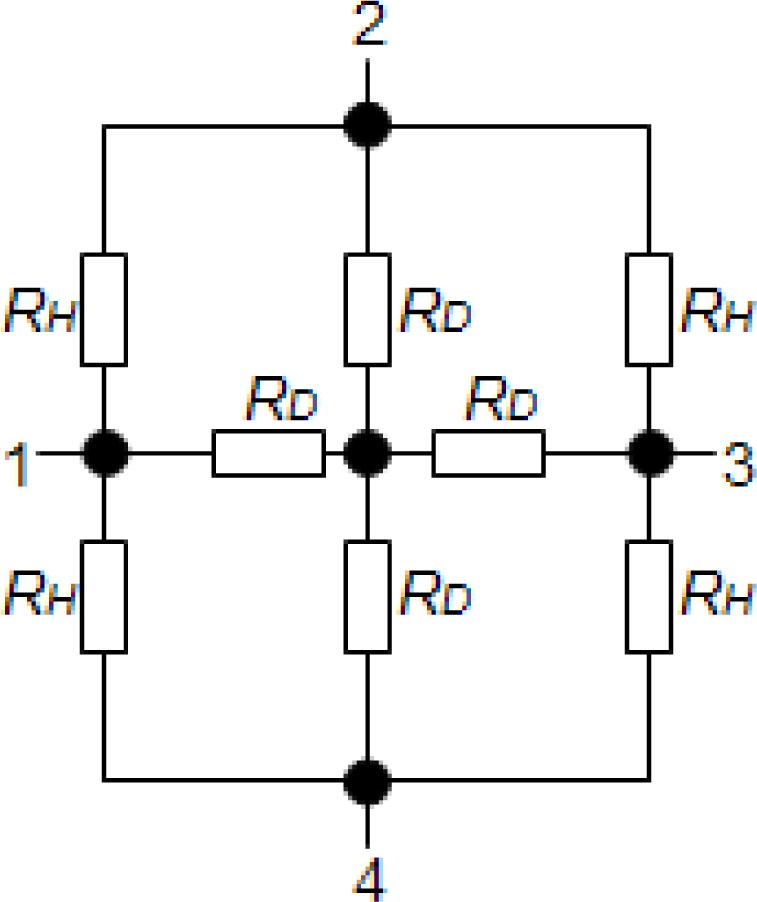
If the fourth contact is applied to the reference ground, the Z-matrix of the 90° symmetry Hall plate is only decided by three parameters Z11, Z12, Z13. If the input current I1 is applied to the first contact, the three measuring potentials shown in Figure 1 have the following relation: U1 – U2 = U3, and then we can obtain Z11 – Z12 = Z13. As a result, 90° symmetry Hall plates require at least two types of resistances to model their electrical properties. Thus, an 8-resistance model topology for the 90° symmetry Hall plate is suggested, which is illustrated in Figure 2. Its Z-matrix at zero-magnetic field is expressed by:
However, in the conventional 4-resistance Wheatstone bridge model [4,5], the diagonal resistances RD are often neglected. The value of the resistance between two adjacent contacts is not accurate because current lines linking the two adjacent contacts do not flow across the center of the device. But this problem can be solved well in the 8-resistance model so that the simulation accuracy can be improved.
2.1. The Structure of the Model
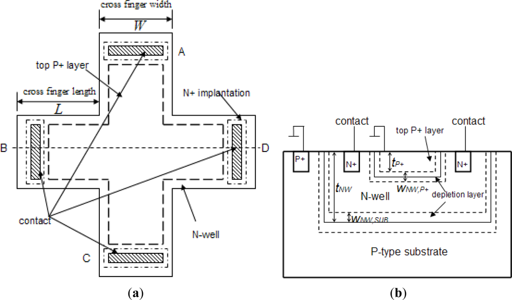
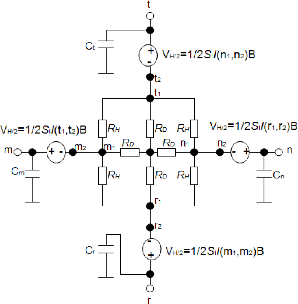
The 90° symmetry cross-shaped Hall plate (see Figure 3) is most widely used because of its high sensitivity and immunity to alignment tolerances resulting from the fabrication process. Its fabrication technology is fully compatible with the standard CMOS process. As shown in Figure 3(a), the active area of the cross-shaped Hall plate is usually realized by a weakly doped N-well diffusion region. The N-well is isolated from the P-type substrate by the reverse-biased well/substrate p-n junction. A shallow heavily doped top P+ layer often covers the surface of active area to decrease the flicker noise and the surface losses. It is normally formed to create the source and drain regions of PMOS transistors [9]. In addition, four contact regions are highly N+ doped to reduce the contact resistances in the source and drain formation processing step for NMOS transistors. Based on the basic model topology shown in Figure 2, a new simplified 8-resistance model for the CMOS integrated cross-shaped Hall plate is developed, as shown in Figure 4. Compared with Dimitropoulos’ model, the simulation model is improved by replacing the JFETs by N-well body resistances and depletion capacitances. The four depletion capacitances are added into the model to simulate the transient behavior of the Hall plate. Besides, there are four controlled voltage sources VH/2 to model the Hall voltage. Each Hall voltage source VH/2 is controlled by the electrical current flowing through the nearer contact.
In order to determine the resistance values of RH and RD in our model, a new and simple computation method is proposed in contrast to the FEM simulation method [7]. It is well known that it is best to measure the N-well sheet resistance Rs according to the Van-der-Pauw method. Although the Van-der-Pauw method requires that the contacts of Hall device be point-like, it has been reported that cross-shaped Hall plate with a finger length to width ratio larger than 1:1 can give an accurate Rs value with an error of less than 0.1% [10]. Usually, the required ratio of finger length to width can be fulfilled for achieving a high current related sensitivity. Thus, in the case of symmetric Hall plates, the sheet resistance can be determined by measuring the resistance value RAB,CD in term of Van-der-Pauw method [11]:
On the other hand, according to the structure of the model illustrated in Figure 4, the resistance RAB,CD is calculated by:
The internal resistance between two diagonal contacts is given by:
Here, (2L/W+2/3) is the effective square number of the N-well resistance. L and W are the finger length and finger width of cross-shaped Hall plate, respectively. The center square number is approximately reduced to 2/3 as the two fingers for sensing Hall signal are placed in parallel. Considering the Equations (3), (4) and (5), finally we can obtain:
The N-well sheet resistance Rs is calculated by:
Here, ND,NW is the N-well doping concentration, teff is the effective depth of Hall plate. As shown in Figure 3(b), it is equal to:
Note that there are two main parasitic capacitances distributed across the Hall device body: (1) the reverse-biased upper depletion capacitance between the top P+ layer and N-well; (2) the reverse-biased bottom depletion capacitance between the N-well and p-type substrate. Usually the top P+ layer and P-type substrate are applied to ground together, thus they are connected in parallel physically. Unfortunately, the parasitic capacitances may limit the switching frequency for the spinning current offset reduction method. In order to simulate the complete ac behavior of the Hall plate, these parasitic depletion capacitances should be included in the model. Assuming the one-sided abrupt junctions, each depletion capacitance per unit area is calculated by following Equation (5):
Here, Vbi is the built in potential of PN junction, ND,NW is the doping of N-well, and NA is the doping of top P+ layer or P-type substrate.
2.2. Hall Voltage and Magnetic Sensitivities
When a magnetic field B is orthogonally applied on a device plane and two diagonal contacts are biased with a current I, the Hall effect takes place. Then the hall voltage VH appears on two additional contacts, it is equal to:
When Hall plate is biased with a voltage source V, the Hall voltage is expressed by voltage related sensitivity SV:
The impact of the Hall devices geometry on Hall voltage is modeled by a geometrical correction factor. For a cross-shaped Hall plate, it can be calculated by using a conformal mapping [12]:
In our model illustrated in Figure 4, each Hall voltage VH/2 is modeled by using the current-controlled voltage sources with the following equation:
2.3. Voltage Dependent Non-Linear Effect
It is well known that the thickness of depletion region is obviously changed by the reverse biased PN junction. Therefore, both sheet resistance and magnetic sensitivity suffer from a strong voltage non-linearity dependence. Since the doping concentration of the P+ top layer is obviously higher than that of the P-type substrate, the thickness variation of the upper depletion region modulated by reverse biased voltage can be approximately ignored. Using Equation (8), which is extended by the voltage dependent teff, and a Taylor expansion results up to second order are given by [5]:
With the same calculation method, the current related sensitivity is modeled by:
2.4. Temperature Effect
We know that the temperature drift has serious effects on the equivalent N-well resistance, sensitivities and offset of the Hall device. The temperature behavior of N-well sheet resistance can be well approximated by the second order polynomial:
Since the thermal expansion of silicon is merely 2.6 ppm/°K and the G and teff are considered as temperature independent, the thermal drift efficient of current related sensitivity can be given by [12,13]:
2.4. Piezo-Resistance and Piezo-Hall Effects
When a Hall plate is assembled, its performance is deteriorated by two physical stress-related effects, i.e., piezo-resistance and piezo-Hall effects. The piezo-resistance effect due to packaging stress provokes relative variations of N-well resistances. In combination with technology variation, junction field effects and temperature drift, it is the main source of offset. The sensitivity is also impacted by packaging stress. The variation of sensitivity is called piezo-Hall effect. Considering this effect, Equation (20) can be rewritten as [14,15]:
Since the mechanical stress changes with temperature, the temperature coefficient of sensitivity illustrated in Equation (19) can be rewritten as:
For a plastic packaging, the temperature coefficient related to piezo-Hall effect can be defined by [13]:
3. Comparing Results of Simulation with Experimental Results
The new simulation model code has been written in behavioral Verilog-A language and was tested on a Cadence Spectre simulator tool using AMS 0.8 μm CMOS technological parameters (shown in Table 1) [12]. The finger width and finger length of the cross-shaped Hall plate are designed to 40 μm and 60 μm, respectively.
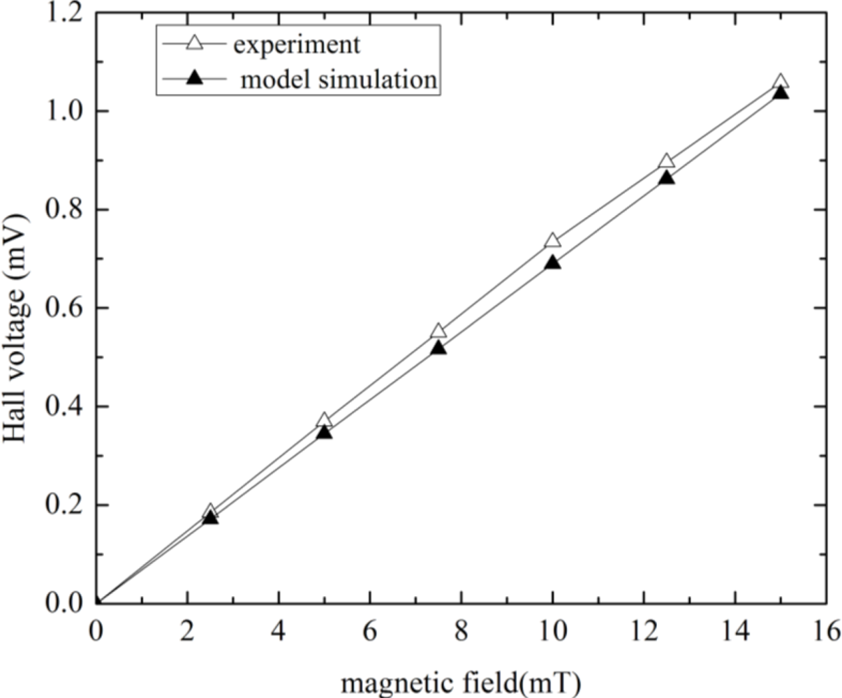
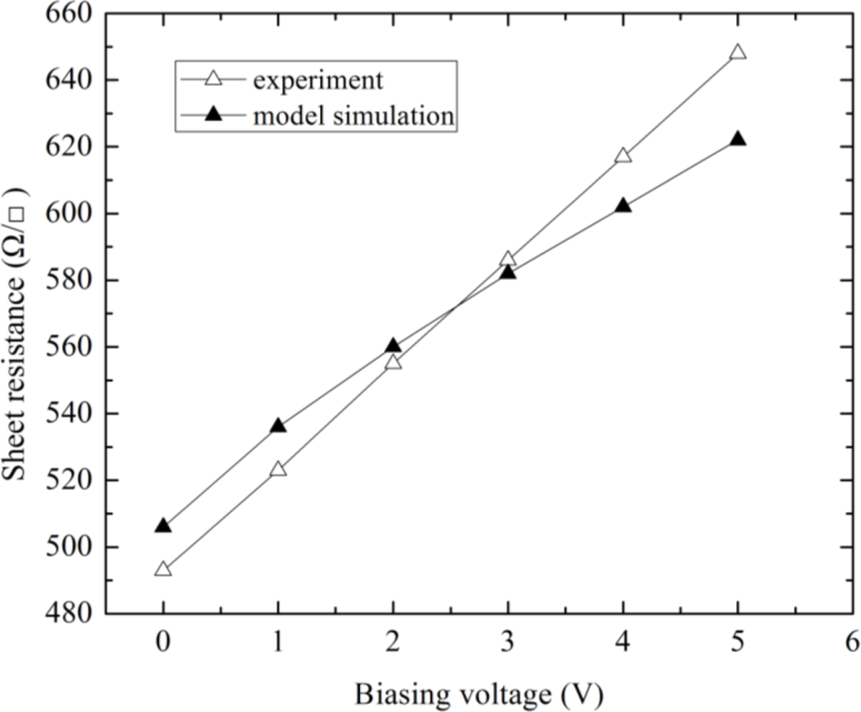
To show the correctness and accuracy of this model, the corresponding experimental results of the Hall plate fabricated using the same technology given in the literature [12] are compared with the model’s simulation results. First, we performed the simulation of Hall voltage versus magnetic field at room temperature. The simulated and test results when the input bias current is 1 mA and the Hall plate is liberated of packaging stress, are plotted in Figure 5. It can be observed that the simulated Hall voltage is proportional to magnetic field intensity. When the magnetic field intensity is 2.5, 5, 7.5, 10, 12.5 and 15 mT, the simulated Hall signal is 0.172, 0.345, 0.517, 0.69, 0.862 and 1.035 mV, respectively. While the value of the measured Hall voltage is 0.185, 0.37, 0.551, 0.735, 0.896 and 1.058 mV for the corresponding magnetic field intensity. We can see that the simulated current-related sensitivity is 69 V/AT, while the tested result is 75 V/AT. A very good agreement is thus obvious in Figure 5. If a mechanical stress in the CMOS Hall plate is estimated at σx = σy= −70 MPa for a typical plastic packaging [14], which will lead to a variation of the simulated magnetic sensitivity of about 5% at room temperature compared with the stress-free sensitivity. Secondly, the simulation of the N-well sheet resistance versus input voltage was implemented at room temperature without packaging stress influence.
Figure 6 illustrates the comparison between the simulated and tested sheet resistances per square versus variation of input voltage (sweeps from 0 V to 5 V). The measured sheet resistance per square changes from 493 Ω/γ to 648 Ω/γ. By comparison, the simulated sheet resistance per square changes in the range (506 Ω/γ–622 Ω/γ) with a small error. In addition, the characteristics of magnetic sensitivity vs. temperature drift were simulated.
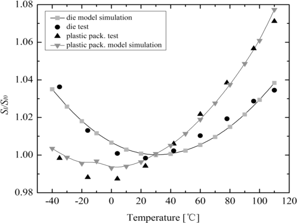
The measured and simulated relative variations of the current-related sensitivity related to the value at room temperature as a function of temperature for the zero-stress mounting of the Hall plate is demonstrated in Figure 7. In this temperature dependence of sensitivity simulation, we assume the zero temperature coefficient αSI of Hall plate takes place at 27 °C, and αSI linearly changes from −500 ppm/°K to +500 ppm/°K in the temperature range from −40 °C to 110 °C. It is obvious that a good accordance is achieved between simulation and experimental results for a die absence of packaging stress influence. Meanwhile, both simulated and tested results of the thermal drift of SI influenced by the plastic packaging stress as a function of temperature are also shown in Figure 7. The simulated thermal drift of SI for a typical plastic package (TSSOP) is also in good agreement with the measured results. It should be pointed out that the piezo-resistance and piezo-Hall effects in packaged Hall sensors are very complex issues, which cannot accurately be modeled by only a small number of key physical and technological parameters. Therefore, a very accurate simulation result cannot be achieved in some cases.
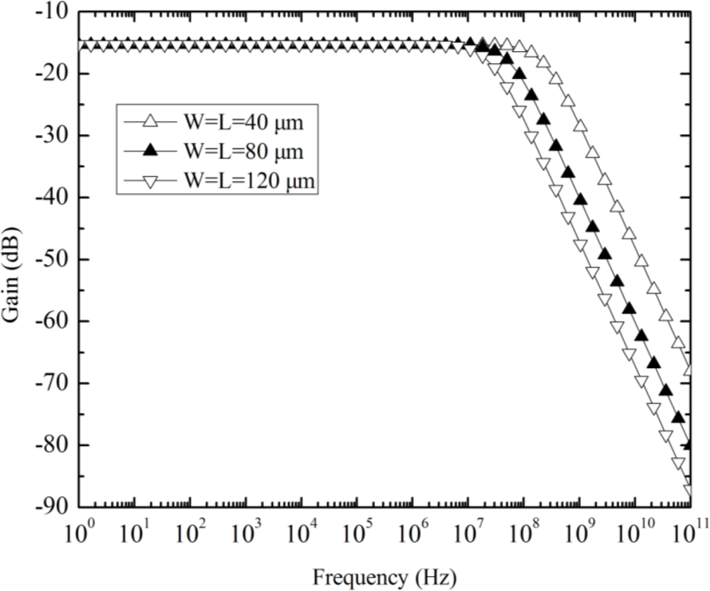
Finally, the ac simulation of the Hall plate was performed at 3 V DC bias. The ratio of finger length to finger width is fixed to 1, while the finger length is taken as a parameter, changing from 40 μm to 120 μm with a step of 40 μm. The simulation results in Figure 8 show that the smaller Hall plate has the higher corner frequency and the −3 dB bandwidth highly exceeds the one MHz range for the largest Hall plate, indicating that any limited frequency response of Hall plate within the working range (usually below 1 MHz) cannot be observed.
4. Conclusions
An equivalent circuit simulation model for a CMOS-integrated Hall plate has been improved. The structure of the model consists of a passive network, including eight non-linear resistances, four depletion capacitances and four current-controlled voltage sources. The model completely takes into account the non-linear conductivity effects, geometrical effects and temperature effects. Meanwhile, the packaging stress influence on Hall plates is also considered to a certain degree. In addition, the model only needs a small number of key physical and technological parameters. The model has been implemented in Verilog-A hardware description language and was successfully tested with the standard EDA tool Cadence. For testing the model correctness and accuracy, the model simulation of a Hall plate were performed using AMS 0.8 μm CMOS technology parameters and are compared with the measured results reported in the literature [12]. A very good agreement is obtained. It should be noted that if those key technological parameters such as N-well sheet resistance, Hall mobility, etc. can be calibrated by the measurements of the Hall sensors fabricated in a standard CMOS technology line, more accurate model simulation results could be achieved.
Acknowledgments
This work was supported by China Jiangsu Science and Technology Support Project (NO.BE2009143).
References
- Boero, G; Demierre, M; Besse, P-A; Popovic, RS. Micro-Hall devices: Performance, technologies and applications. Sens. Actuat. A 2003, 106, 314–320. [Google Scholar]
- Dimitrov, K. 3-D silicon Hall sensor for use in magnetic-based navigation systems for endovascular interventions. Measurement 2007, 40, 816–822. [Google Scholar]
- Bilotti, A; Monreal, G; Vig, R. Monolithic magnetic Hall sensor using dynamic quadrature offset cancellation. IEEE J. Solid-State Circuits 1997, 32, 829–835. [Google Scholar]
- Salim, A; Manku, T; Nathan, A; Kung, W. Modeling of magnetic-field sensitive devices using circuit simulation tools. Proceedings of the 5th IEEE Solid-State Sensor and Actuator Workshop, Hilton Head Island, SC, USA, June 1992; pp. 94–97.
- Schweda, J; Riedling, K. A nonlinear simulation model for integrated Hall devices in CMOS silicon technology. Proceedings of the International Workshop on Behavioral Modeling and Simulation, Santa Rosa, CA, USA, October 2002; pp. 14–20.
- Dimitropoulos, PD; Drljaca, PM; Popovic, RS; Chatzinikolaou, P. Horizontal Hall devices: A lumped-circuit model for EDA simulators. Sens Actuat A 2008, 145–146, 161–175. [Google Scholar]
- Madec, M; Kammerer, JB; Hebrard, L. An improved compact model of cross-shaped horizontal CMOS-integrated Hall-effect sensor. Proceedings of the 8th IEEE International NEWCAS Conference, Montréal, QC, Canada, June 2010; pp. 397–400.
- Ausserlechner, U. Limits of offset cancellation by the principle of spinning current Hall probe. Proceedings of the 3rd IEEE Conference on Sensors, Vienna, Austria, 24–27 October 2004; pp. 1117–1120.
- Xu, Y; Zhao, FF. A simplified simulation model for CMOS integrated Hall devices working at low magnetic field circumstance. Proceedings of the 10th IEEE International Conference on Solid-State and Integrated Circuit Technology (ICSICT), Shanghai, China, September 2010; pp. 1925–1927.
- Cornils, M; Paul, O. Sheet resistance determination of electrically sysmmetric planar four-terminal devices with extended contacts. J. Appl. Phys 2008, 104, 024503. [Google Scholar]
- Cornils, M; Doelle, M; Paul, O. Sheet resistance determination using symmetric structures with contacts of finite size. IEEE Trans. Electron. Devices 2007, 54, 2756–2761. [Google Scholar]
- Demierre, M. Improvements of CMOS Hall Microsystems and Application for Absolute Angular Position Measurements. Ph.D. Thesis. Ecole Polytechnique Federale De Lausanne, Lausanne, Switzerland, 2003. [Google Scholar]
- Manic, D; Petr, J; Popovic, RS. Temperature cross-sensitivity of Hall plate in submicron CMOS technology. Sens. Actuat. A 2000, 85, 244–248. [Google Scholar]
- Fischer, S; Wilde, J. Modeling package-induced effects on molded Hall sensors. IEEE Trans. Adv. Packag 2008, 31, 594–603. [Google Scholar]
- Herrmann, M; Ruther, P; Paul, O. Piezo-Hall characterization of integrated Hall sensors using a four-point bending bridge. Procedia Eng 2010, 5, 1376–1379. [Google Scholar]


| Parameters Definition Default value |
| ND,NW Doping in N-well 4 × 1016 cm−3 |
| NA,P+ Doping in top P+ layer 1 × 1020cm−3 |
| NA,SUB Doping in substrate 1 × 1016cm−3 |
| tNW Depth of N-well 4 μm |
| tP+ Depth of top P+ layer 0.3 μm |
| μn Electrons mobility 950 cm2/V.s |
| μH Hall mobility 1,200 cm2/V.s |
| RTC1 First temperature coefficient of N-well resistance 1%/°K |
| RTC1 Second temperature coefficient of N-well resistance 20 ppm /°K |
| P12 Piezo-Hall coefficient 40 × 10−11 Pa−1 |
| αSI Temperature coefficient of SI ±500 ppm/°K |
| αpiezo-Hall Temperature coefficient of piezo-Hall effect −450 ppm/°K |
© 2011 by the authors; licensee MDPI, Basel, Switzerland. This article is an open access article distributed under the terms and conditions of the Creative Commons Attribution license (http://creativecommons.org/licenses/by/3.0/).
Share and Cite
Xu, Y.; Pan, H.-B. An Improved Equivalent Simulation Model for CMOS Integrated Hall Plates. Sensors 2011, 11, 6284-6296. https://doi.org/10.3390/s110606284
Xu Y, Pan H-B. An Improved Equivalent Simulation Model for CMOS Integrated Hall Plates. Sensors. 2011; 11(6):6284-6296. https://doi.org/10.3390/s110606284
Chicago/Turabian StyleXu, Yue, and Hong-Bin Pan. 2011. "An Improved Equivalent Simulation Model for CMOS Integrated Hall Plates" Sensors 11, no. 6: 6284-6296. https://doi.org/10.3390/s110606284