Effect of Annealing Temperature on the Optical Spectra of CdS Thin Films Deposited at Low Solution Concentrations by Chemical Bath Deposition (CBD) Technique

Abstract
:1. Introduction
2. Experimental
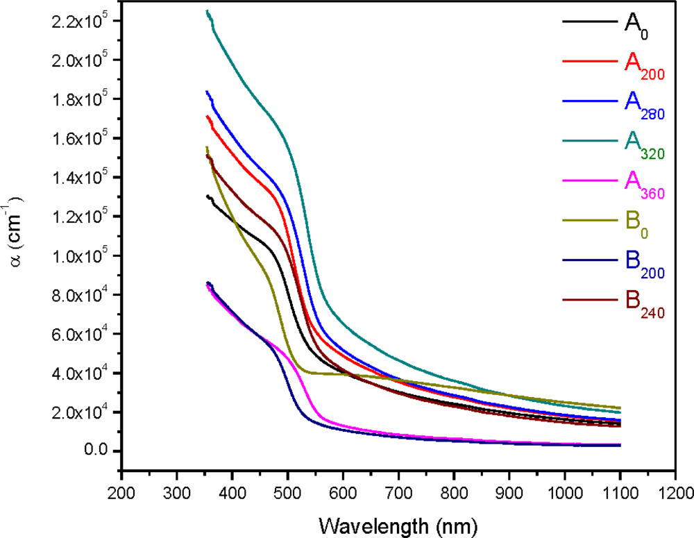
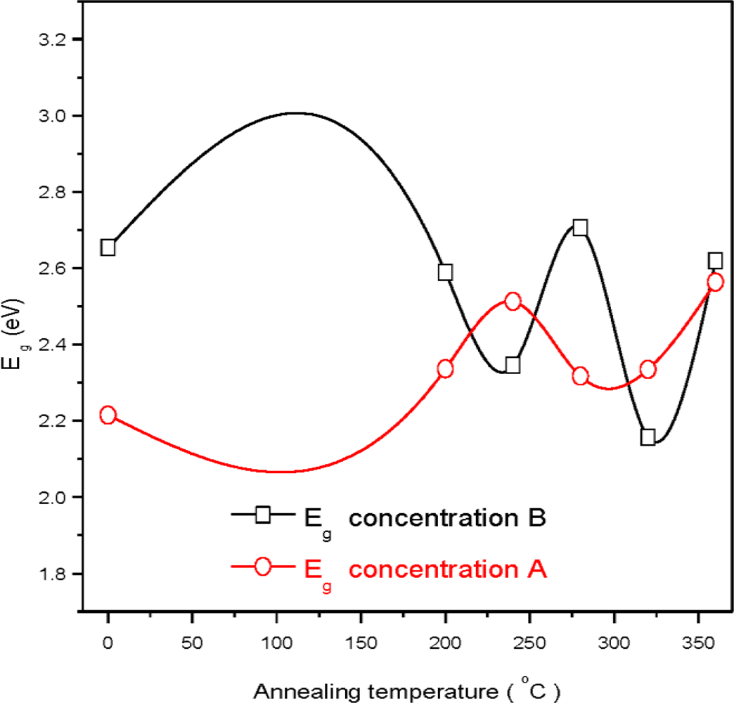
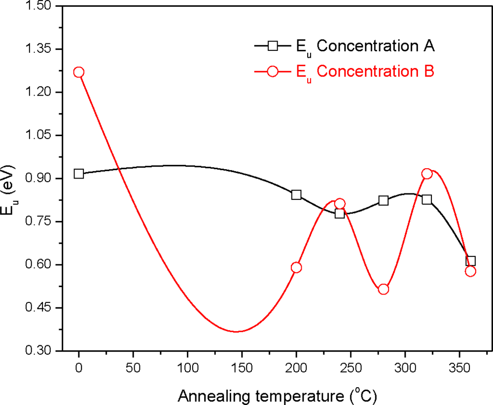
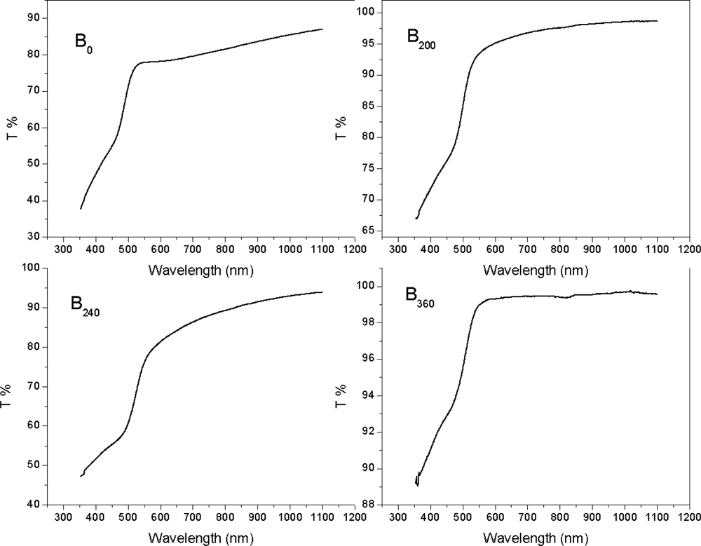
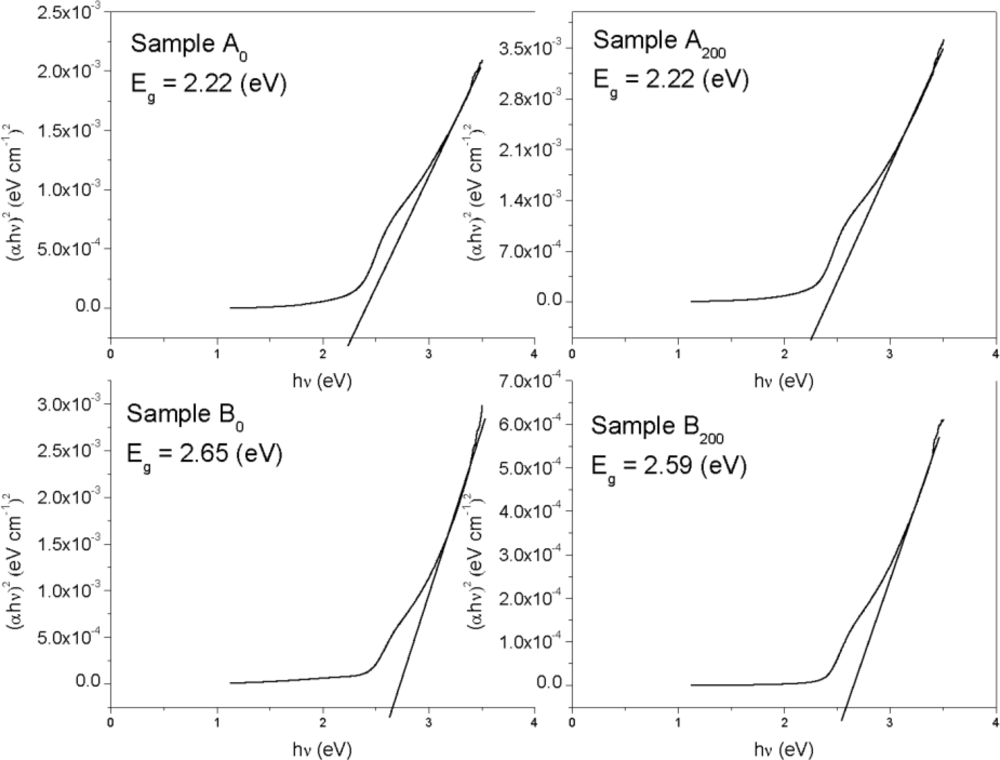
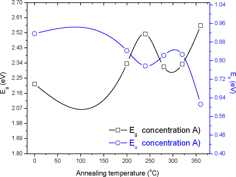
3. Results and Discussion
4. Conclusions
Acknowledgments
References
- Khallif, H; Isaiah, O; Chai, G; Chow, L. Characterization of CdS thin films grown by chemical bath deposition using four different cadmium sources. Thin Solid Films 2008, 516, 7306–7312. [Google Scholar]
- Bertino, MF; Gadipalli, RR; Story, JG; Williams, CG; Zhang, G; Sotiriou-Leventis, C; Tokuhiro, AT; Guha, S; Leventis, N. Laser writing of semi conductor nanoparticles and quantum dots. Appl. Phys. Lett 2004, 85, 6007–6010. [Google Scholar]
- Zhang, J; Sun, L; Liao, S; Yan, C. Size control and photoluminescence enhancement of CdS nanoparticles prepared via reverse micelle method. Solid State Commun 2002, 124, 45–48. [Google Scholar]
- Hodes, G; Albu-Yaron, A; Decker, F; Motisuke, P. Three-dimensional quantum-size effect in chemically deposited cadmium selenide films. Phys. Rev. B 1987, 36, 4215–4221. [Google Scholar]
- Contreras, MA; Egaas, B; Ramanathan, K; Hiltner, J; Swartzlander, A; Hasoon, F; Noufi, R. Progress toward 20% efficiency in Cu(In,Ga)Se2 polycrystalline thin-film solar cells. Res. Appl 1999, 7, 311–316. [Google Scholar]
- Khallif, H; Oladej, IO; Chow, L. Optimization of chemical bath deposited CdS thin films using nitrilotriacetic acid as a complexing agent. Thin Solid Films 2008, 516, 5967–5973. [Google Scholar]
- Oladeji, I; Chow, L; Ferekides, C; Viswanathan, V; Zhao, Z. Matter/CdTe/CdS/Cd1−xZnxS/TCO/glass: A new CdTe thin film solar cell structure. Sol. Energy Mater. Sol. Cells 2000, 61, 203–211. [Google Scholar]
- Contreras, M; Romero, M; To, B; Hasoon, F; Noufi, R; Ward, S; Ramanathan, K. Optimization of CBD CdS process in high-efficiency Cu(In,Ga)Se2-based solar cells. Thin Solid Films 2002, 403, 204–211. [Google Scholar]
- Chu, TL; Chu, SS; Ferekides, C; Wu, CQ; Britt, J; Wang, C. High efficiency thin film CdS/CdTe heterojunction solar cells. J. Cryst. Growth 1992, 117, 1073. [Google Scholar]
- Ferekides, C; Britt, J. CdTe solar cells with efficiencies over 15%. Sol. Energy Mat. Sol. Cells 1994, 35, 255–262. [Google Scholar]
- Kaur, I; Pandya, DK; Chopra, L. Growth kinetics and polymorphism of chemically deposited CdS films. J. Electrochem. Soc 1980, 127, 943–948. [Google Scholar]
- Froment, M; Lincot, D. Phase formation processes in solution at the atomic level: Metal chalcogenide semiconductors. Electrochim. Acta 1995, 40, 1293–1303. [Google Scholar]
- Gutiérrez, LCD; Rosendob, E; Ortegaa, M; Olivac, AI; Tapiab, O; Díazb, T; Juárezb, H; Garcíab, G; Rubínd, M. Structural analysis of CdS thin films obtained by multiple dips of oscillating bath. Mat. Sci. Eng. B 2009, 165, 74–76. [Google Scholar]
- Caglar, M; Caglar, Y; Ilican, S. The determination of the thickness and optical constants of the ZnO crystalline thin film by using envelope method. J. Optoelectron. Adv. Mater 2006, 8, 1410–1413. [Google Scholar]
- Prabahar, S; Dhanam, M. CdS thin films from two different chemical baths-structural and optical analysis. J. Cryst. Growth 2005, 285, 41–48. [Google Scholar]
- Sanap, VB; Pawar, BH. Optical study of the effect of cadmium sources on nano-crystalline CdS thin films. Chalcogenide Lett 2010, 7, 227–231. [Google Scholar]
- Ghosh, T; Bandyopadhyay, S; Roy, KK; Kar, S; Lahiri, AK; Maiti, AK; Goswami, K. Optical and structural properties of lead iodide thin films prepared by vaccum evaporation method. Cryst. Res. Technol 2008, 43, 959–963. [Google Scholar]
- Morris, GC; Vanderveen, R. Cadmium sulphide films prepared by pulsed electrodeposition. Sol. Energy Mater. Sol. Cells 1992, 27, 305–319. [Google Scholar]
- Zelaya-Angel, O; Alvarado-Gil, JJ; Lozada-Morales, R; Varga, H; Ferreira da Silva, A. Band-gap shift in CdS semiconductor by photoacoustic spectroscopy: Evidence of a cubic hexagonal lattice transition. Appl. Phys. Lett 1994, 64, 291–294. [Google Scholar]
- Murali, KR; Matheline, M; John, R. Characteristics of brush electrodeposited CdS films. Chalcogenide Lett 2009, 6, 483–490. [Google Scholar]
- Sasikala, G; Thilakan, P; Subramanian, C. Modification in the chemical bath deposition apparatus, growth and characterization of CdS semiconducting thin films for photovoltaic applications. Sol. Energy Mater. Sol. Cells 2000, 62, 275–293. [Google Scholar]
- Liu, F; Lai, Y; Liu, J; Wang, B; Kuang, S; Zhang, Z; Li, J; Liu, Y. Characterization of chemical bath deposited CdS thin films at different deposition temperature. J. Alloys Compd 2010, 493, 305–308. [Google Scholar]
- Moualkia, H; Hariech, S; Aida, MS. Structural and optical properties of CdS thin films grown by chemical bath deposition. Thin Solid Films 2009, 518, 1259–1262. [Google Scholar]
- Kurik, MV. Urbach rule. Phys. Status Solid A 1971, 8, 9–45. [Google Scholar]


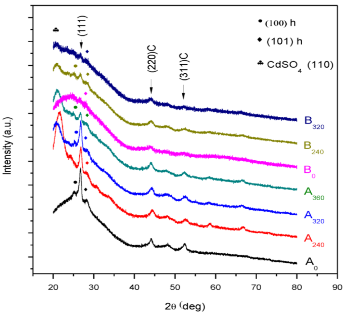
| Sample | 2θ (Deg.) (hkl) | CdS Structure |
|---|---|---|
| A0 | 26.7277°(111), 44.1346°(220), 52.3619°(311) | cubic (ref: 01-080-0019) |
| 25.1618°(100), 28.2306°(101), 48.1229°(103) | hexagonal (ref: 01-080-0006) | |
| B0 | 26.4962°(111), 43.9355°(220), 51.9702°(311) | cubic (ref: 01-075-1546) |
| 28.1727°(101) | hexagonal (ref: 00-065-3414). | |
| A200 | 26.8079°(111), 44.4133°(220), 52.7364°(311) | cubic (ref: 01-075-0581) |
| 28.6450°(101), 58.4937°(202), 66.7578°(203) | hexagonal (ref: 01-080-0006). | |
| B200 | 26.7070°(111), 44.2175°(220), 52.4116°(311) | cubic (ref: 01-080-0019) |
| 24.6784°(100), 28.3841°(101), 58.4548°(202), 66.6981°(203) | hexagonal (ref: 01-089-2944). | |
| A240 | 26.8176°(111), 30.8886°(220), 44.4089°(311 | cubic (ref: 01-075-1546) |
| 58.5947°(202), 66.8296°(203) | hexagonal (ref: 01-080-0006). | |
| B240 | 26.6935°(111), 44.0913°(220), 52.3710°(311) | cubic (ref: 01-075-1546) |
| 25.0745°(100), 28.4921°(101) | hexagonal (ref: 00-001-0783). | |
| A280 | 26.7905°(111), 30.7475°(200), 44.4319°(220), 52.5711° (311), 73.2311°(420) | cubic (ref: 01-080-0019) |
| 24.7269°(100), 28.3734°(101), 48.0309°(103), 58.6591° (202), 66.8441°(203) | hexagonal (ref: 01-077-2306). | |
| B280 | 25.5707°(111), 30.3946°(200), 44.1649°(220) | Cubic (ref: 00-042-1411) |
| 28.1785°(101), 47.5271°(103), 58.3791°(202), 66.5891°(203) | hexagonal (ref: 01-080-0006). | |
| A320 | 26.8012°(111), 44.2445°(220), 52.5047°(311) | cubic (ref: 01-080-0019) |
| 25.3195°(100), 28.5660°(101), 58.3476°(202) | hexagonal (ref: 00-001-0783). | |
| B320 | 26.5834°(111), 44.0583°(220), 52.1528°(311) | cubic (ref: 01-080-0019) |
| 28.4385°(101) | hexagonal (ref: 01-075-1545). | |
| A360 | 26.7119°(111), 43.9950°(220), 52.2836°(311 | cubic (ref: 01-080-0019) |
| 24.9576 °(100), 28.2761°(101), 58.2849°(202) | hexagonal (ref: 01-080-0006). | |
| B360 | 43.7486°(220) | cubic (ref: 00-065-2887). |
| 24.6729°(100) | hexagonal (ref: 00-006-0314) |
© 2011 by the authors; licensee MDPI, Basel, Switzerland. This article is an open-access article distributed under the terms and conditions of the Creative Commons Attribution license (http://creativecommons.org/licenses/by/3.0/).
Share and Cite
Rizwan, Z.; Zakaria, A.; Ghazali, M.S.M.; Jafari, A.; Din, F.U.; Zamiri, R. Effect of Annealing Temperature on the Optical Spectra of CdS Thin Films Deposited at Low Solution Concentrations by Chemical Bath Deposition (CBD) Technique. Int. J. Mol. Sci. 2011, 12, 1293-1305. https://doi.org/10.3390/ijms12021293
Rizwan Z, Zakaria A, Ghazali MSM, Jafari A, Din FU, Zamiri R. Effect of Annealing Temperature on the Optical Spectra of CdS Thin Films Deposited at Low Solution Concentrations by Chemical Bath Deposition (CBD) Technique. International Journal of Molecular Sciences. 2011; 12(2):1293-1305. https://doi.org/10.3390/ijms12021293
Chicago/Turabian StyleRizwan, Zahid, Azmi Zakaria, Mohd Sabri Mohd Ghazali, Atefeh Jafari, Fasih Ud Din, and Reza Zamiri. 2011. "Effect of Annealing Temperature on the Optical Spectra of CdS Thin Films Deposited at Low Solution Concentrations by Chemical Bath Deposition (CBD) Technique" International Journal of Molecular Sciences 12, no. 2: 1293-1305. https://doi.org/10.3390/ijms12021293