
A Review on Fundamentals of Noise-Shaping SAR ADCs and Design Considerations
by
 , , and
Victor H. Arzate-Palma
1,2,* ,
,
David G. Rivera-Orozco
1,2,
Gerardo Molina Salgado
2 and
Federico Sandoval-Ibarra
1,* 1
Advanced Studies and Research Center (CINVESTAV), National Polytechnic Institute (IPN), Av. del Bosque 1145, Zapopan 45019, Mexico
2
Microelectronic Circuits Centre Ireland, T12 R5CP Cork, Ireland
*
Authors to whom correspondence should be addressed.
Chips 2024, 3(2), 153-181; https://doi.org/10.3390/chips3020007
Submission received: 1 February 2024
/
Revised: 23 March 2024
/
Accepted: 6 May 2024
/
Published: 10 May 2024
(This article belongs to the Topic Advances in Microelectronics and Semiconductor Engineering)
Abstract
:A general overview of Noise-Shaping Successive Approximation Register (SAR) analog-to-digital converters is provided, encompassing the fundamentals, operational principles, and key architectures of Noise-Shaping SAR (NS SAR). Key challenges, including inherent errors in processing circuits, are examined, along with current advancements in architecture design. Various issues, such as loop filter optimization, implementation methods, and DAC network element mismatches, are explored, along with considerations for voltage converter performance. The design of dynamic comparators is examined, highlighting their critical role in the SAR ADC architecture. Various architectures of dynamic comparators are extensively explored, including optimization techniques, performance considerations, and emerging trends. Finally, emerging trends and future challenges in the field are discussed.
1. Introduction
The 21st century has pushed the capabilities of any analog-to-digital converter (ADC) to the limit, caused by the growing demand for various applications in low-power devices and the need to extend the life of batteries [1,2,3]. In practice, both the applications and their respective requirements are an open problem because current developments are powered with low voltages (<1.1 V). The challenge is to design architectures that are tolerant to the effect of these and other sources of error. Up to date, various types of ADCs have been implemented to push their performance to the limit and meet the requirements that each application demands; outstanding is the search for low power consumption and the number of bits that impacts the signal-to-noise and distortion ratio (SNDR) and the oversampling ratio (OSR), among other characteristics. It is important to note that many of these metrics are correlated; Figure 1 illustrates the main ADC architectures in terms of their bandwidth and resolution [4,5,6,7,8].
For certain applications, preserving the minimum power consumption is a crucial key, and SAR is the best exponent due to the reduced hardware used in its construction, a characteristic that can be seen in Figure 2, where the power consumption against the sampling frequency, , in SAR, NS SAR, and Sigma Delta implementations, which are continuous-time (CT) and switched-capacitor (SC) [9], is shown. SAR has demonstrated an adequate balance in power consumption, moderate bit resolution (≈14 bits), and SNDR. However, many implementations have been limited to 80 dBs of SNDR. To increase this metric, the quantization error feedback is used in combination with the oversampling technique to apply “noise shaping” in the SAR, always keeping a low power consumption. This quality has made the NS SAR an attractive option for its integration in system-on-chip (SoC) interfaces and its manufacturing feasibility in nanometric CMOS technologies, where efforts have been focused on improving the BW [10]. In practice, NS SAR is not an ideal converter. At the circuit level, there are a series of implications that affect the linearity of the converter, which impacts the overall performance of the ADC. These drawbacks have led to a redesign of SAR A/D conversion, and this explains why new proposals have replaced continuous consumption circuits with switched proposals. In this way, sources that introduce nonlinearities into the conversion process are also eliminated and limited to using at least one active system, the voltage comparator, whose performance is purely dynamic. Today, optimizing the performance of the comparator is an open problem, and it seeks to increase its performance without incorporating static consumption circuits.
This document is divided into four sections. Section 2 presents the fundamentals of NS SAR ADC. Section 3 presents the main non-idealities of the NS SAR ADC, the problems and challenges to overcome. Relevant proposals that have recently added to the design of the dynamic comparator are described in Section 4, where their advantages/disadvantages are analyzed. Finally, Section 5 presents both the conclusions of this work and trends in NS-SAR A/D conversion.
2. From SAR ADC to NS SAR: Fundamentals
Understanding the operation of NS SAR is easier by starting with the analysis of a traditional SAR ADC structure shown in Figure 3. The A/D conversion system is based on a binary search algorithm, and with each conversion cycle it gets closer to the input value. The DAC is usually built with capacitive networks (CDAC) for its ease of scaling and its simple construction. The single-ended format for a 4-bit CDAC is shown in Figure 4; the operating principle is based on charge distribution and the generation of weighted voltages. The system includes two phases: sampling and conversion. The first phase captures the value of , and all capacitors are connected by , such that one plate of the capacitor is connected to Vin and the other to GND. In the conversion stage, because the process starts with the N-bit midscale, the voltage at the inverting terminal of the comparator, , will be determined by Equation (1); a representation of the capacitive voltage divider in the first cycle can be seen in Figure 5.
Note that this result assumes that the comparator is not only ideal, but that the weighted sum is not affected by the switching frequency, i.e., it is a noiseless analysis. It is important to note that the comparator is designed according to the characteristics of the ADC and the CDAC. Figure 4b and Figure 5b show two types of single-output comparators. The first is a comparator implemented with a conventional differential amplifier, and the second is a comparator based on a switched amplifier. These comparators will be explained in detail in Section 4. Regardless of the sampling topology (bottom plate (a) or top plate (b), see Figure 6), at present the CDAC implementations are fully differential, because they benefit not only from noise rejection in the common mode, but also an improvement in the signal voltage range can be seen. The differential input signals can be defined as in Equations (2) and (3), where x is an arbitrary voltage; the voltage reference is “split”, as per what is shown in Equations (4) and (5).
The principle of operation of a fully differential structure is similar to the single-ended version, but now an identical capacitive network is added in the non-inverting terminal to process the “negative” signal. After the sampling phase (in both networks), the conversion cycles start at the midscale of the N bits. For example, in the 4-bit scheme shown in Figure 6b, the top network will have the 8C capacitor connected to Vrefp, and the other capacitors connected to , i.e., the digital word 10,000, while the bottom network will always have the complement, in this case, the digital word 01111. Thus, the voltages on the comparator are determined by Equations (6) and (7). The comparator evaluates if < , if true, then the output will be a logical ‘1’, otherwise it will be a logical ‘0’. Now, depending on the result of that comparison, a new digital word value will be evaluated in the next cycle. Suppose the comparison result was ‘1’, so now in the next evaluation it will be 11000 for the upper network and 00111 for the lower network. Thus, capacitive networks modify their voltage divider and now the voltages will model Equations (8) and (9) at the input of the comparator; this process is repeated N times. A complete scheme of the 4-bit fully differential binary search algorithm can be seen in Figure 7. Once the conversion process is finished, A/D conversion is completed. However, the accuracy of the conversion is determined by the quantization process (and resolution), and since this is a non-linear process, a residual voltage remains due to the difference between the sampled input and the digital conversion estimate (in analog format). At the end of the conversion there will be a difference, or quantization error, <1 LSB. An open problem is to further reduce that value, so that the conversion increases its degree of linearity.
Figure 8 illustrates the comparison voltages at each cycle of a 10-bit SAR ADC. With the natural progression in the conversion process, the voltages get closer to , and eventually, in one extra cycle, the quantization error can be processed in differential format.
The experienced reader will be able to evoke what happens analogously in a modulator, where the main feature lies in oversampling and error feedback, to apply noise shaping to the quantization noise.
The distinctive feature of a NS SAR is the sampling and processing of the CDAC residual voltage (quantization error) and applying the noise-shaping technique using a filter. The technique distributes not only the quantization noise outside the BW of interest, but also shapes the comparator noise. This residue, or quantization error, is added to the conversion line to perform a noise shaping, where the synthesis of the various architectures has preference to those that include low consumption. A NS SAR consists of a SAR structure, a feedback filter for residual voltage processing, and a summation point for adding the quantization error to the conversion line. There are two main architectures for loop filter implementation and residual processing: Error Feedback (EF) and Cascade Integrator Feed-Forward (CIFF) [11,12], illustrated in Figure 9 and Figure 10, respectively.
2.1. Noise-Shaping SAR ADC Implementations: Error-Feedback and Cascade Integrator Feed-Forward
The block diagram of EF and CIFF structures are presented in Figure 11 and Figure 12, respectively. Signal and noise transfer function analysis can be deduced from these diagrams, obtaining (10) and (11) for EF and CIFF, respectively. The noise transfer function NTF(z) can be identified as the factor that multiplies the quantization error (z), being (1−(z)) for EF and (1+(z) for CIFF.
EF implementations require a summing point to add the sampled signal and the quantization error, and the synthesis of this block determines the efficiency of the NTF [11]. The loop filter implementation can be active or passive [13]. Some recent reports [14,15] have incorporated a unity gain buffer instead of passive sampling to achieve lossless NTF. In these works, the use of ping-pong schemes for switching is adopted, which facilitates fully passive implementations. Table 1 presents a comparison of important reported EF implementations.
The latter metric allows for a punctual and “fair” comparison between the performance of the ADCs. This is the Figure of Merit (FoM) and it represents a relationship between resolution, conversion speed, and power consumption. There are two main FoMs for ADCs, Walden’s (12) and Schreier’s (13). The units of the first are J/conv-step and of the second, decibels. A lower FoM value indicates a lower value in power consumption with the same noise performance, which also implies a lower overall power consumption [16].

Table 1.
Comparative performance of EF implementations.
| Specification | Chen 2015 [13] | Li 2018 [17] | Yi 2022 [14] |
|---|---|---|---|
| Filter | EF | EF | EF |
| Process | 65 nm | 40 nm | 65 nm |
| Order | 1 | 2 | 1 |
| Supply | 0.8 V | 1.1 V | 1.2 V |
| Bits | 8 | 9 | 9 |
| BW | 6.25 MHz | 625 kHz | 625 kHz |
| OSR | 4 | 8 | 16 |
| SNDR | 58.03 dB | 79 dB | 81 dB |
| Power | 120.7 µW | 84 µW | 183.6 µW |
| FoMs | 165.1 dB | 178 dB | 176.3 dB |
It is important to note that the number of CIFF implementations is greater than EF. The first report of a NS SAR was a CIFF structure [18]. In practice, the filter implements FIR-IIR for residual voltage processing, since the IIR stage provides additional gain. Note that in a CIFF implementation, for the quantization noise in Equation (11) to have a high-pass characteristic as in EF, (z) multiplied by should have the nature of an integrator (/()). This answer is an ideal representation, but in practice this does not happen. An equation that better models losses is (14). With a large value of , the zero of NTF(z) is located closer to the unit circle, as illustrated in Figure 13, which allow for a more defined noise-shaping effect. However, to achieve a higher value , a precise charge transfer is required in the integrator [19], which is generally based on the use of high-gain and high-BW OTAs. This type of implementation opposes the original idea of a NS SAR, which is to have a low power consumption and be scalable in CMOS technologies.
Concerning active implementations, those integrators with op-amps and switched capacitors (SC) stand out [18,20]. An active third-order approach proposed in [21] can be seen in Figure 14. That work is important because it uses duty cycling to reduce power consumption. In passive implementations, the issue is that there is no gain, and seeking to overcome this inconvenience, DA and capacitor stacking are the main architectures (Figure 15 and Figure 16) since they offer low power consumption amplification [22,23]. However, DA gain is sensitive to PVT variations. Digital calibration is used to ensure PVT robustness, but it increases design complexity [24]. Implementations that include buffers [25] have also been used to deal with attenuation due to charge transfer. The source–follower topology is commonly used, but there are also modified versions such as the one described in [26]. Other works include a pre-amplifier, as mentioned in [27], but also pseudo-differential architectures of inverter-based circuits [28]. The scheme of a fully passive implementation is mentioned in [19]. Finally, it is important to point out that recent works incorporate the Closed-Loop DA [29] and the Ring Amplifier [30] as promising structures due to their robustness.
It is well known that the implementation of higher orders in the EF NTF(z) (greater than 2) is complicated because the FIR filter coefficients increase in quantity and are more sensitive to variation. For this reason, nested–cascade architectures have been proposed [31]. Hybrid third-order implementations combining EF and CIFF have also been reported [32,33], where both feedback and feed-forward addition are included. Because of the flexibility in the implementation of the IIR filter, recent resonators, CRFF (Cascade Resonator Feed-Forward), have been proposed [34], but also one that includes the resonator in a hybrid architecture (active–passive), achieving an improvement in BW [35]. A comparison of the cascaded implementations can be seen in Table 2.
2.2. Noise-Shaping Plots
The benefit of oversampling is that noise outside the band of interest can be filtered out from all noise-generating sources. However, it is necessary to process the noise that falls inside the band. Combining oversampling and quantization error feedback, noise shaping is achieved, and the idea is to have a lower value of noise in the band of interest. As an illustrative case, consider a SAR ADC with a 10-bit core, fs = 100 MHz, amplitude = 0.45 V, offset = 0.5 V, and BW of 1 MHz simulated behaviorally in MATLAB-Simulink® [36]. The process for plotting the power spectral density consists of applying a window to the output data, obtaining the fast Fourier transform (FFT), and then plotting the resulting spectrum. Figure 17 shows the power spectral density with SNDR, SNR and ENOB metrics for a traditional SAR ADC (Nyquist). If an EF structure is adopted and the quantization error is fed back in addition to a delay to the input sampled signal, the first-order noise shaping, presented in Figure 18 and Figure 19, is achieved. Do not forget that an OSR must be defined for noise shaping to make sense. For illustrative purposes, it has been set to 16, although common OSRs for NS SAR range from 4 to 8. From the aforementioned plots, it is important to note two features: the slope of the noise shaping (20 dB/decade), and within the BW of interest (1 MHz), the noise has a higher attenuation compared to the Nyquist SAR. Also note the increment in the values of the performance metrics, approximately 30 dB in SNDR and SNR and just over 5 bits in ENOB.
But, how to get NTF(z) implementations of higher orders? Recalling Equation (10), it has been seen that if (z) is equal to unity, and only the quantization error is fed back with a delay, a first-order shaping is achieved. Now, what should be the value of (z), to have a second-order NTF(z), ()2? If a filter that models (2) is implemented, as can be seen in Equation (15), NTF(z) will shape the quantization noise at a rate of 40 dB/decade, as shown in Figure 20. Similarly, to get a third-order NTF(z), (z) must be equal to (+ ), as shown in Equation (16). Figure 21 presents the PSD plot for a third-order implementation.
3. Non-Idealities in the Performance of NS SAR ADC: Problems, Challenges and Solutions
In practice, A/D conversion systems are oriented towards silicon synthesis. Beyond the challenges that the topologies themselves impose on the implementation (on the passive or active filters, on the comparator, etc.), it must be considered that the different sources of error add non-linearity to the converter.
Table 3 presents the main problems of NS SAR, as well as the solutions and techniques used to date. In general, it is known that the disadvantage of noise shaping is that all loop filters introduce thermal noise, which is not shaped. Regarding the implementations, it is necessary to mention that although the dynamic multi-input comparator has been a well-accepted technique, its disadvantage is that each input represents a noise source. But, the most important noise sources influencing the nonlinearity of the NS SAR ADC are CDAC mismatch, kT/C noise, flicker, and comparator offset.
3.1. Mismatch in CDAC
CDAC binary weighted capacitors are manufactured in two ways in MOS technologies: metal–insulator–metal (MIM) and metal–oxide–metal (MOM). Both are subject to variations in physical parameters (due to the manufacturing process) and are the cause of the error that contributes to the CDAC non-linearity. By not having exact capacitor values (and their weights), non-uniform conversion code widths are generated. This is because the unit capacitance is intended to be minimal to benefit power consumption. In contrast, as the technologies scale, the unit capacitances are of a smaller value, increasing the standard deviation. Therefore, the error also increases, becoming so severe that the conversion error (after calibration) can be greater than 1 LSB [37]. Illustratively, the non-linearity of the conversion process can be seen in Figure 22. The need to incorporate techniques that mitigate the impact and manage the effects of mismatch is evident. To appreciate the impact of the mismatch on the NS SAR, Figure 23 shows the PSD of the EF NS SAR presented in Figure 19, but with a CDAC capacitive mismatch of 1%. Note that the metrics have decreased from the performance shown in Figure 19, SNDR at about −9 dB and ENOB at −1.5 bits. SFDR is the ratio of the amplitude of the input signal to the amplitude of the largest spurious signal in the frequency range of interest. Ideally, a pure signal has the power concentrated at its fundamental frequency. However, due to the non-linearity of the components, there is an undesirable value of third harmonic distortion in fully differential architectures [1]. There are various techniques for correcting the mismatch (see Table 3). Although increasing the area of the capacitors solves the mismatch problem, it is not feasible because it is not scalable. Digital calibration (foreground and background) is a common technique; here, it is required to previously know an estimate of the error due to mismatch. LMS (Least Mean Squared) [17,37,38] is a digital calibration method that has generated remarkable values of SFDR. This calibration method can be of the foreground or background type. Its operation is based on the fact that it obtains the exact weight of each capacitor in the CDAC network (from the conversion results) and corrects the errors with the calibrated weights. With digital techniques, values of up to 105 dB of SFDR have been achieved [39].
Mismatch Error Shaping (MES) has also been a good alternative. This is a total analog implementation and 105 dB of SFDR have been reported [40]. Its operating principle focuses on the fact that the mismatch error is fed back and conformed with a high-pass filter function, (1). To achieve this, the key is to preset the CDAC LSBs in NS SAR before sampling, so that the mismatch error from previous conversions is captured during sampling, as shown in Figure 24. Note that the MSB is not fed back, i.e., GND is naturally conserved, since it is considered to be a precise reference. Then, the LSBs are reset and the natural conversion continues [20]. The general idea is that the preset LSBs from the previous conversion are subtracted from the current signal [12] and then a first-order shaping (17) is achieved. Also, redundancy LSBs can be added to correct the so-called DAC settling.
A drawback of using MES is the overrange, produced by the extra voltage added to the input of the converter, which should not exceed the limits of and [41]. Recent MES techniques have adopted a two or three-level predictive process to correct overrange and compensate for extra voltage. In the first-order MES works reported in [16,41], values of 98 dB of SFDR have been obtained; it has also been demonstrated that a second-order shaping can be achieved, reaching values of SFDR as high as 122 dB [42]. Other alternatives such as the use of the double sampling technique [40] and pre-comparison [43] have reported values of 104.5 dB and 103 dB, respectively.
An alternative for mismatch correction is Dynamic Element Matching (DEM), which uses algorithms to select unitary components and average the elements. Figure 25 illustrates the operation of the DEM, where the digital output signal is encoded on a thermometric scale, and with the implemented algorithm, the selection of unitary components is applied. Note that the implementation can be excessive as the number of bits increases. Data Weighted Averaging (DWA) is a remarkable algorithm, but there are also Butterfly Randomization, Individual Level Averaging, and Tree Structure techniques. For example, a combination of DEM and Dither [21] reported 112 dB of SFDR, where the disadvantage is a BW of 2 kHz.
The operating principle of the DWA is based on the selection of elements in a rotating manner, so that the output value of the CDAC is the sum of the unit elements selected cyclically. The selection ensures that the mismatch error is averaged as fast as possible, in such a way that they are modulated with a high-pass filter function, (), as described in Equation (18) [44]. Figure 26 presents an example of the DWA algorithm for a 3-bit DAC, which corresponds to eight unit elements. In each cycle the selection of the first element is made from the element that follows after the last selected element of the previous cycle (for example, in the first cycle the input code is 1, and in the second cycle it is 3, but three elements are selected from element 1, that is, from element 2 to 4), that is why the “pointer” is implemented, because in each new conversion cycle the pointer is updated, and it is necessary to know the value of the last selected element so that the current error is subtracted from the past error [45]. However, combinations of both techniques have been used, DWA for the most significant bits and MES for the least significant, and thus compensate the disadvantages of each one. The most significant works that incorporate this combination of techniques have reached outstanding values [20,23,46]. Table 4 summarizes the main implementations according to the technique used and the SFDR value achieved.
3.2. CDAC Mismatch Correction, an Alternative: NS DEM
The block diagram of the NS SAR with the different error sources is presented in Figure 27. (z) is the sampling error (mostly kT/C noise); ) represents quantization errors, comparator noise, and DAC settling; is the DAC mismatch error; and and are the noise errors referring to the input of the filters themselves. The signal transfer function, , the noise transfer function N and (associated with and with , respectively), are equal to unity. Regardless of whether the EF or CIFF filter option is used, note how, since , the mismatch error is not shaped. Now, if a block L(z) is added, the noise transfer function referring to the mismatch error would be described by Equation (19). If that block has a high-pass function, (), the mismatch error can be placed outside the BW. The challenge is the synthesis of circuits for L(z), which should be added to the system to model this filter. This idea has already been applied to a modulator [51].
3.3. CDAC Mismatch Correction, an Alternative: NS DEM
kT/C noise is another problem where the efforts to obtain better metrics are focused. During the sampling process, thermal noise with a total power of kT/C “sneaks” into the sampled signal. Solutions include the design of an input buffer [52] (to alleviate the load on the input source), increasing the value of the unit capacitors, active cancellation [53], and also improvements in the design of the CMOS switch with bootstrapping [54] and clock boosting [55] techniques. The noise in the comparator is another problem of interest, because it can be a limiting factor in the resolution of the quantizer. Tri-Level Voting schemes have been applied to reduce noise. This technique is preferred over Majority Voting [24] because it takes advantage of more information in the comparator output data and provides an additional decision level, and because in the last two conversion cycles (corresponding to the LSB), it will repeatedly activate the comparator four times for each bit, then the result will be determined. By doing so, the comparator noise must be suppressed through averaging [19].
Another technique for noise reduction in the comparator is the appropriate selection of the comparator architecture (such as a chopped transconductor), where switches are incorporated to generate a square wave modulator, also known as chopping modulation [56], in such a way to shift the low-frequency spectrum out of the BW. The offset is amplified, passes through the modulator, and is removed by a low-pass filter. The disadvantage of this technique is that the added square signal has to be exactly 50% duty cycle, so that it does not provide a residual DC signal; glitches are also generated by the effect of charge injection and coupling of clock systems. A NS SAR has been used in the input buffer and in the IIR filter [20].
4. Trends on Dynamic Comparison
4.1. CMOS Comparators
Comparators are an essential block in many mixed-signal circuits, especially in the analog-to-digital converter (ADC). In an ADC, the comparator plays an important role, serving as the conversion bridge between the physical and digital worlds. The performance in low-power ADCs, such as successive–approximation–register (SAR) ADCs, strongly depends on the comparator’s performance. This includes characteristics such as noise, offset, common-mode voltage, influence accuracy, and resolution, while the comparison speed determines the sampling rate of an ADC [57]. Typically, between 40% and 60% of the power consumption in a SAR ADC is due to the comparator [58,59,60,61]. With the development of manufacturing processes and the trend towards decreasing supply voltage, strict requirements are imposed on quantization noise, making energy consumption reduction a challenge, assuming that comparators are not scalable unlike digital blocks in a SAR ADC. The comparator, as a fundamental part in power contribution, must have sufficient gain to reduce input-referred noise (IRN), be insensitive to common-mode voltage () and PVT variations, as well as have low power consumption.
The comparator, as it was originally understood, has evolved and its design is becoming more complex every day because it now must perform more tasks. Figure 4b shows the conventional two-stage, continuous-time comparator, which is based on an uncompensated Miller topology. Although one of its drawbacks is the offset, properly dimensioning the output stage, and specifically the transistor, it is possible to reduce the offset to acceptable values; in this proposal all transistors operate in strong inversion. However, for low-power applications it is unsuitable because of its static dissipation. Currently the complexity in designing a comparator can be reduced a little by defining its application, that is, by establishing the bandwidth of the signal and the resolution of the converter of which it is part. In other words, the comparator is custom designed, which means that the necessary technology is available for its implementation. One option to reduce power consumption is the CMOS 3.3 V simple-switched amplifier. Figure 5b shows the two- and three-stage design, where – are parasitic capacitances and the and transistors are responsible for making the voltage comparison. Note that the voltage of is formed by the voltages to be compared. For illustrative purposes consider the two-stage comparator, marked with the shaded area. First, assume that the initial value of is and is high, therefore is switched off. In this condition is precharged to and is discharged to 0 V. When varies from to 0 V, there is a time in which turns on and discharges. That voltage is amplified by , which is an inverter amplifier. To restore the phase, another amplifier is used, which apparently favors the rapid response of the comparator. Let us suppose the output should have a large swing, from 0 to 3.3 V, as the input changes ±1.0 mV. So, the required gain is just 3.3 V/2 mV = 1650 ≡ 64.35 dB [62]. However, this proposal is not suitable for low-voltage and low-power consumption because noise affects the converter’s resolution.
As we know, electronic noise, offset, mismatch, power consumption, sampling rate, and non-linearity of network elements, to name a few unwanted effects, affect the precision of the conversion in different proportions, that is, it is very important to know which are the most relevant sources of error and focus the greatest effort there. Nowadays, using comparators based on the operation of a latch is common practice. On the one hand, power consumption benefits, now being a dynamic consumption. This characteristic, on the other hand, causes the comparator to perform an amplification task and then another of comparison. Although the tasks are defined in each clock cycle, the aim is to optimize energy efficiency in each comparison, so that energy consumption is efficient in each conversion step. Therefore, as the trend in SAR ADCs is low power consumption, dynamic comparators are the best option.
A dynamic comparator shown in Figure 6c (without transistors ) is an example of a latch-based comparator that is periodically regenerated. In this proposal the comparator also draws current from only when the state changes. This way, the energy needed to change the state is as small as in a digital gate. In practice this comparator would provide a large output swing that is well suited for the digital processing following the comparator. Now, the basic operation can be described in three phases. First, do not consider the transistors and , and assume that . In this phase the capacitors and are precharged to and , respectively, and while and are on and are off. In the second phase the capacitances and begin their discharge. That voltage in and flows as the current to and , respectively. In the third phase the signal through and with the load is amplified with a factor corresponding to a cascode inverter amplifier, causing to ground and to . It can be verified that if the current extracted from each capacitance () is constant, the approximate gain is:
where is the output impedance and , with ,; is the time the amplification lasts. It is important to say that the input transistors () operate in the triode region, which is relevant because when the latch is regenerated () the currents of both transistors are steered so that the logical state of is established. However, the mismatch in resistance associated with transistors affects the expected state, causing a slow response. One solution is to reduce both the equivalent resistance and mismatch by including the transistors, also operating on triode and where and are bias voltages. In this proposal the input voltage that causes both resistors to be equivalent is the threshold voltage of the comparator [55]:
the one that can be adequately proposed by the designer. However, the noise generated by the comparator is inversely proportional to the efficiency, , and to minimize this undesirable effect, a higher value of gm or equivalently greater gain is required (see Equation (22)). But, because the bias current is strongly related to the voltage of and the common-mode input efficiency is compromised. Consequently, one solution is to have independent control of both the latch and amplifier function.
4.2. StrongARM Latch
Within the state of the art, one of the most used comparators in recent years is the StrongARM Latch (SA) [63]. Its popularity stems from being the first single-stage latch-type comparator (the pre-amplification stage and latch are in a single block), not consuming static power, producing rail-to-rail outputs, and having input-referred noise (IRN) dependent on the input differential pair. However, because it lacks isolation between the latch block and the differential input, the SA latch exhibits kickback noise, which hampers performance and energy efficiency [63]. The classic SA latch is depicted in Figure 28.
It can be observed that transistors and implement the pre-amplifier stage, while the two cross-coupled pairs and and the four switches – implement the latch stage. Its operation can be summarized in two phases, the reset phase and the amplification phase. In the reset phase, when CLK = 0 (low state), transistors and are turned off, and the transistors operating as switches – are turned on, precharging nodes , , , with a value equal to . When CLK = 1 (high state), – are turned off, and and are turned on, allowing a differential current proportional to () to flow from the capacitors . Here, the amplification operation occurs in which the comparator provides gain and works as a dynamic integrator, where the input signal is continuously integrated by the capacitor . The amplification phase has an approximate time represented by:
where is the common-mode current and is the threshold voltage of the NMOS transistors. The voltage gain is represented by:
where it is observed that the gain depends on the efficiency of of and . The voltage at nodes , decreases to a value of , and then transistors are turned on and allow the current to flow from output nodes and , where the potential of these nodes reaches a value of at which point transistors are turned on. The positive feedback from these transistors eventually leads one of the outputs to return to , while the other drops to GND. The comparator noise is represented by:
where it can be observed that to reduce thermal noise, a high value of is needed, as well as a large value of . It is observed that to design a low-noise comparator, it is necessary to have a large-gain . There are certain disadvantages, such as the limitation of low voltage, energy waste due to the total discharge of , the voltage gain is limited by the value of , and because transistor is biased in the weak inversion region, the current is strongly correlated with the common-mode input voltage (), making the comparator performance susceptible to variations in .
4.3. Double-Tail Comparator
The double-tail comparator presented in [64] is shown in Figure 29. This comparator avoids the kickback issue by separating the pre-amplifier stage from the latch stage . It features independent control of the common-mode current for both the pre-amplifier and the latch, achieved through the addition of separate tail transistors , resulting in a shorter delay in the output response. During the reset phase (CLK = 0), and are turned off. Transistors pre charge nodes and to , causing transistors to discharge output nodes and to GND. During the amplification phase (CLK = 1), and are turned on, are turned off, and voltages at nodes and gradually discharge to GND. During the reset phase, these nodes must be charged from ground to , resulting in an energy consumption equal to . A drawback of the double-tail comparator is that latch transistors operate in the linear region, reducing the effective gain between stages, leading to increased noise and offset [59]. Using this same structure, Babayan et al. [65] performed a delay analysis for dynamic comparators and proposed a new version of the double-tail comparator with low-voltage and low-power characteristics. The main idea is to increase the output voltage variation to reduce delay. For this purpose, two control transistors are added in parallel with cross-coupled.
4.4. Dynamic Two-Stage Comparator
On the other hand, the architecture of the dynamic two-stage comparator [59] shown in Figure 30a features a separation between the input blocks, comprising the amplification stage (–) with an input differential pair (/) and the second stage (–) which includes a simple voltage amplifier (/) and a positive feedback amplifier to achieve rail-to-rail digital output. This comparator operates in two phases, reset and amplification. The reset stage occurs when CLK = 0, where the capacitors connected to nodes are charged to , and the outputs fall to GND. When CLK = 1, the amplification phase occurs. The differential output voltage increases, while the common-mode voltage output decreases to GND. As approaches the threshold voltage of the PMOS transistor, the input differential pair of the second stage starts amplifying, thus, while the differential output of the second stage increases, positive feedback ensures rail-to-rail outputs. Power dissipation in the first stage stops when has discharged completely. Power dissipation in the second stage stops when the positive feedback amplifier has settled. When the clock signal CLK returns to low, all nodes (/,/) are pre-charged to their original values. Therefore, this comparator virtually has no energy dissipation when the comparator is inactive. The first stage of the comparator improves the energy efficiency of the system because it is considered to operate in the weak inversion region. This gain significantly reduces the input noise of the second stage. On the other hand, the capacitors connected to the output nodes are fully discharged, which still implies evident energy consumption in each comparison process.
4.5. Dynamic Bias Comparator
The architecture of the dynamic bias comparator is presented in [66]. The architecture is shown in Figure 30b and is similar to Figure 30a, with the exception that the transistor is replaced by a transistor , a tail capacitor , and a transistor . The idea of this architecture, in addition to reducing energy consumption, is to obtain an increase in the gain factor. The topology includes capacitors ( and ) that perform two functions. On the one hand, they are useful to control charge and discharge, and on the other hand, they minimize the effect of thermal noise. It should be noted that the transistors operate in weak inversion, so the current is very small and thus increases the gain. This proposal not only increases the efficiency but also the input referred noise (IRN) is now inversely proportional to , (see Equation (26)). In other words, now does not represent a parasitic capacitance but rather a capacitor that is selected for a particular gain and a desired SNR [66]. One drawback of this architecture is that it exhibits higher delay compared to the SA latch [64]. Another inconvenience arises in corner process analysis or in large common-mode input voltage variations, causing the integration phase to become unstable.
4.6. FIA-Based Comparator
The Floating Inverter Amplifier-based comparator is proposed in [67], comprising a pre-amplifier floating inverter amplifier (FIA) and a SA latch. The architecture can be seen in Figure 31. It is robust against corner process variations and common-mode input voltage fluctuations. It utilizes a reserve capacitor , which is charged during the reset phase to a value of and serves as a power source during the integration phase. It also optimizes energy efficiency and is resilient to PVT variations. It is an architecture that provides isolated voltage to the amplifier (–). The input and output currents of must be equal (), yielding a common-mode current , hence achieving a constant output common-mode voltage without a CMFB circuit. This is an important point, maintaining a constant output common-mode voltage, as it can limit the accuracy of the comparator and consequently the resolution of the ADC.
The transconductance is expressed as:
where is the instantaneous current of the transistor with a small differential input voltage, n is the slope factor in weak inversion, and is the thermal voltage. The differential output voltage can be approximated as:
The source voltage , and the change is obtained as follows:
The integration gain is calculated as:
The IRN of the FIA at the end of the integration time can be calculated as:
As can be observed, the IRN is inversely proportional to , demonstrating that with higher gain, the noise effect decreases. It is also observed that using a large , as well as large changes in , increases the gain. Therefore, with the FIA serving as the pre-amplification stage, it provides sufficient gain to reduce IRN. However, this topology exhibits a limited response speed [67,68]. To address this speed limit, a modification to the FIA-SA is performed in [68], enhancing both gain and response speed while preserving the advantages of the FIA pre-amplifier, achieved through the utilization of a latch-embedding floating amplifier (LEFA). In [68], a design approach is described to achieve higher gain in the first stage by placing the input pair in a parallel latch configuration. This configuration allows for positive feedback resulting in greater gain and faster decision-making.
4.7. Low-Power Comparator
In [58], a modification to the dynamic two-stage comparator is proposed, adding a cross-coupling mechanism around the input differential pair, which prevents the complete discharge of the comparator’s internal nodes when small differential signals are present at the input, thus reducing energy consumption per comparison. It is worth noting that this architecture does not use additional capacitors like the FIA-SA [67] or the DB [66].
As observed in Figure 32, the pre-amplification stage features two transistors with cross-coupling ( and ) and two additional transistors acting as switches ( and ). During the reset phase, the pre-charge transistors (, , , and ) drive the , , , and nodes to , while transistors and reset the output nodes of the regenerative latch ( and ). With turned off, the current flow from to GND is cut off.
The amplification phase consists of two sub-phases. In the first sub-phase, the gates of and are connected to , causing node to discharge rapidly due to the drop in across the switches ( and ). Node behaves similarly. Transistors and start conducting current flow, and and operate in the linear region. This causes the voltage at the intP and intN nodes to decrease, and the voltage at and to increase slowly, resulting in changes in the differential input pair’s voltage, reducing transconductance . This behavior may increase the conversion time for small differential input voltages. In the second sub-phase, the circuit changes its behavior as the node becomes static. This results in a reduced discharge speed of the node. The operational timing behavior ensures that and are only discharged to specific voltages below , improving energy efficiency compared to conventional architectures.
This architecture achieves higher energy efficiency without additional capacitors or complex logic, based on a simple cross-coupling mechanism around the differential input pair. However, this approach results in a slight increase in noise.
In general, it can be concluded that one of the trends in the design of the comparator is to prevent the capacitances in the output nodes from being completely discharged. This property minimizes energy consumption, increases the gain, and reduces the effect of thermal noise. Consequently, the proposed topologies experience an increase in the number of transistors, and capacitors are even manufactured to improve the performance of the comparator and the systems in general. Some proposals do not include capacitors but add more transistors that operate as switches. Cross couplings and separation of functions are other characteristics of comparators that increase the complexity of behavioral analysis as well as analytical analysis to quantify various figures of merit. However, models of design have been obtained that not only depend on parameters that are under the control of the designer, but also on some fundamental technological parameters. But, nothing has been said about the temperature T, this being a parameter that directly affects the generation of thermal noise. It is not the subject of this contribution to incorporate the analysis of the comparator in the face of temperature variations, including evaluating the performance of the system at cryogenic temperatures. But, much in the design of A/D conversion circuits still remains to be said.
5. Trends, Further Advances, and Conclusions
It is a fact that for certain critical applications, NS SAR can be considered as a natural substitute for conventional discrete time modulators [12]. However, despite its great low power consumption characteristic, for mainly applications, a wider BW and higher resolution are required. For this reason, it has also been opted for approaches where architecture hybridizations are carried out, and without a doubt in the future there will be implementations with higher BW, low power consumption, and devices that exceed the 100 dB SNR barrier. From the latter, solutions have been developed to increase the sampling frequency without losing BW. The idea is to have more than one ADC, and operate multiple connection channels and overlap their conversions [69]. Another idea is to use the NS SAR as a quantizer in a continuous-time SD modulator [70] and improve the overall performance of the ADC. Undoubtedly, the idea to achieve higher order NTFs that has recently reported more guidelines and contributions, it is NS SAR Multi-stage noise-shaping (MASH) architectures. Figure 33 shows the schematic of a MASH 2-2 without OTA [71] based on an EF structure, it has achieved a fourth-order NTF at 500 kHz BW. Similarly, other interesting works on MASH have been reported [72,73]. Incremental NS SAR implementations should not be neglected either, as they may be promising architectures in the near future [74,75].
It is also interesting how the use of buffers has become indispensable in the circuit design and how Dynamic Level Shifting has been used in a subrange NS SAR [52] to adjust the output of the buffer, in addition to applying a correction to the so-called Inter-Symbol Interference (ISI) which also causes CDAC mismatch. This correction technique is proposed to further improve linearity. However, it must be considered that the comparator in a SAR A/D consumes a high percentage of energy. And, if it is also considered that the development of manufacturing processes tends to reduce the power supply, the designer must not only propose appropriate conversion architectures, but also design active blocks with minimum energy consumption. The best example is the comparator, whose performance has been improved with the development of technology. As an example, today’s comparators, compared to the pioneer two-stage, have reduced energy consumption by approximately 86%. But, not everything has been said. Energy savings possibly lie in reducing, in a controlled manner, the operating temperature, for example, why not a few degrees Kelvin.
Author Contributions
Investigation, V.H.A.-P., D.G.R.-O. and F.S.-I.; Methodology, V.H.A.-P., D.G.R.-O. and F.S.-I.; Resources, F.S.-I. and G.M.S.; Writing—original draft, V.H.A.-P., D.G.R.-O. and F.S.-I.; Writing—review & editing, V.H.A.-P., D.G.R.-O., G.M.S. and F.S.-I. All authors have read and agreed to the published version of the manuscript.
Funding
This research received no external funding.
Institutional Review Board Statement
Not applicable.
Informed Consent Statement
Not applicable.
Data Availability Statement
Data are contained within the article.
Acknowledgments
V.H.A.-P. and D.G.R.-O. would like to thank CONAHCYT for the scholarship support received during their Ph.D. studies.
Conflicts of Interest
The authors declare no conflicts of interest.
References
- Choi, C.; Lee, J.-W. An 11.8-fJ/Conversion-Step Noise Shaping SAR ADC with Embedded Passive Gain for Energy-Efficient IoT Sensors. Sensors 2022, 22, 869. [Google Scholar] [CrossRef] [PubMed]
- Chen, D.; Cui, X.; Zhang, Q.; Li, D.; Cheng, W.; Fei, C.; Yang, Y. A Survey on Analog-to-Digital Converter Integrated Circuits for Miniaturized High Resolution Ultrasonic Imaging System. Micromachines 2022, 13, 114. [Google Scholar] [CrossRef] [PubMed]
- Leene, L.B.; Letchumanan, S.; Constandinou, T.G. A 68μW 31kS/s Fully-Capacitive Noise-Shaping SAR ADC with 102 dB SNDR. In Proceedings of the IEEE International Symposium on Circuits and Systems (ISCAS), Sapporo, Japan, 26–29 May 2019; pp. 1–5. [Google Scholar]
- Lu, R.; Flynn, M.P. A 300MHz-BW 38mW 37dB/40dB SNDR/DR Frequency-Interleaving Continuous-Time Bandpass Delta-Sigma ADC in 28 nm CMOS. In Proceedings of the Symposium on VLSI Circuits, Kyoto, Japan, 13–19 June 2021; pp. 1–2. [Google Scholar]
- Bolatkale, M.; Breems, L.J.; Rutten, R.; Makinwa, K.A.A. A 4GHz CT ΔΣ ADC with 70dB DR and −74dBFS THD in 125MHz BW. In Proceedings of the International Solid-State Circuits Conference, San Francisco, CA, USA, 20–24 February 2011; pp. 470–472. [Google Scholar]
- Ginsburg, B.P.; Chandrakasan, A.P. Highly Interleaved 5b 250MS/s ADC with Redundant Channels in 65nm CMOS. In Proceedings of the International Solid-State Circuits Conference—Digest of Technical Papers, San Francisco, CA, USA, 3–7 February 2008; pp. 240–610. [Google Scholar]
- Kull, L.; Luu, D.; Menolfi, C.; Morf, T.; Francese, P.A.; Braendli, M.; Kossel, M.; Cavrero, A.; Ozkaya, I.; Toifl, T. A 10-Bit 20–40 GS/S ADC with 37 dB SNDR at 40 GHz Input Using First Order Sampling Bandwidth Calibration. In Proceedings of the Symposium on VLSI Circuits, Honolulu, HI, USA, 18–22 June 2018; pp. 275–276. [Google Scholar]
- Zheng, Z.; Wei, L.; Lagos, J.; Martens, E.; Zhu, Y.; Chan, C.-H.; Craninckx, J.; Martins, R.P. 16.3 A Single-Channel 5.5 mW 3.3GS/s 6b Fully Dynamic Pipelined ADC with Post-Amplification Residue Generation. In Proceedings of the IEEE International Solid-State Circuits Conference (ISSCC), San Francisco, CA, USA, 16–20 February 2020; pp. 254–256. [Google Scholar]
- ADC Performance Survey 1997–2021. Available online: http://web.stanford.edu/~murmann/adcsurvey.html (accessed on 22 March 2022).
- Lin, Y.-Z.; Lin, C.-Y.; Tsou, S.-C.; Tsai, C.-H.; Lu, C.-H. 20.2 A 40MHz-BW 320MS/s Passive Noise-Shaping SAR ADC with Passive Signal-Residue Summation in 14nm FinFET. In Proceedings of the IEEE International Solid-State Circuits Conference (ISSCC), San Francisco, CA, USA, 17–21 February 2019; pp. 330–332. [Google Scholar]
- Salgado, G.M.; O’Hare, D.; O’Connell, I. Recent Advances and Trends in Noise Shaping SAR ADCs. IEEE Trans. Circuits Syst. II Express Briefs 2021, 68, 545–549. [Google Scholar] [CrossRef]
- Jie, L.; Tang, X.; Liu, J.; Shen, L.; Li, S.; Sun, N.; Flynn, M. An Overview of Noise-Shaping SAR ADC: From Fundamentals to the Frontier. IEEE Open J. SSCS 2021, 1, 149–161. [Google Scholar] [CrossRef]
- Chen, Z.; Miyahara, M.; Matsuzawa, A. A 9.35-ENOB, 14.8 fJ/conv.-step fully-passive noise-shaping SAR ADC. In Proceedings of the Symposium on VLSI Circuits, Kyoto, Japan, 17–19 June 2015; pp. C64–C65. [Google Scholar]
- Yi, P.; Zhu, Z.; Xu, N.; Fang, L.; Hao, Y. A Unity-Gain Buffer Assisted Noise-Shaping SAR ADC Based on Error-Feedback Structure. Chin. J. Electron. 2022, 31, 658–664. [Google Scholar] [CrossRef]
- Yi, P.; Liang, Y.; Liu, S.; Xu, N.; Fang, L.; Hao, Y. A 625kHz-BW, 79.3dB-SNDR Second-Order Noise-Shaping SAR ADC Using High-Efficiency Error-Feedback Structure. IEEE Trans. Circuits Syst. II Express Briefs 2022, 69, 859–863. [Google Scholar] [CrossRef]
- Li, H.; Shen, Y.; Xin, H.; Cantatore, E.; Harpe, P. A 7.3-μW 13-ENOB 98-dB SFDR Noise-Shaping SAR ADC with Duty-Cycled Amplifier and Mismatch Error Shaping. J. Solid-State Circuits 2022, 57, 2078–2089. [Google Scholar] [CrossRef]
- Li, S.; Qiao, B.; Gandara, M.; Pan, D.Z.; Sun, N. A 13-ENOB Second-Order Noise-Shaping SAR ADC Realizing Optimized NTF Zeros Using the Error-Feedback Structure. IEEE J. Solid-State Circuits 2018, 53, 3484–3496. [Google Scholar] [CrossRef]
- Fredenburg, J.; Flynn, M. A 90MS/s 11MHz bandwidth 62dB SNDR noise-shaping SAR ADC. IEEE Int. Solid-State Circuits Conf. 2012, 47, 468–470. [Google Scholar]
- Li, S.; Liu, J.; Guo, W.; Sun, N. Chapter 2: Noise-Shaping SAR ADCs. In Next-Generation ADCs, High-Performance Power Management, and Technology Considerations for Advanced Integrated Circuits, Advances in Analog Circuit Design 2019; Baschirotto, A., Harpe, P., Makinwa, K., Eds.; Springer: Cham, Switzerland, 2020; pp. 21–40. [Google Scholar]
- Shu, Y.-S.; Kuo, L.-T.; Lo, T.-Y. An Oversampling SAR ADC with DAC Mismatch Error Shaping Achieving 105 dB SFDR and 101 dB SNDR Over 1 kHz BW in 55 nm CMOS. J. Solid-State Circuits 2016, 51, 2928–2940. [Google Scholar] [CrossRef]
- Obata, K.; Matsukawa, K.; Miki, T.; Tsukamoto, Y.; Sushihara, K. A 97.99 dB SNDR, 2 kHz BW, 37.1 µW noise-shaping SAR ADC with dynamic element matching and modulation dither effect. In Proceedings of the Symposium on VLSI Circuits, Honolulu, HI, USA, 15–17 June 2016; pp. 1–2. [Google Scholar]
- Zhang, Y.; Liu, S.; Tian, B.; Zhu, Y.; Chan, C.-H.; Zhu, Z. A 2nd-Order Noise-Shaping SAR ADC with Lossless Dynamic Amplifier Assisted Integrator. Trans. Circuits Syst. II Express Briefs 2020, 67, 1819–1823. [Google Scholar] [CrossRef]
- Liu, J.; Wang, X.; Gao, Z.; Zhan, M.; Tang, X.; Sun, N. 9.3 A 40kHz-BW 90dB-SNDR Noise-Shaping SAR with 4× Passive Gain and 2nd-Order Mismatch Error Shaping. In Proceedings of the International Solid-State Circuits Conference, San Francisco, CA, USA, 16–20 February 2020; pp. 158–160. [Google Scholar]
- Zhuang, H.; Guo, W.; Liu, J.; Tang, H.; Zhu, Z.; Chen, L.; Sun, N. A Second-Order Noise-Shaping SAR ADC with Passive Integrator and Tri-Level Voting. J. Solid-State Circuits 2019, 54, 1636–1647. [Google Scholar] [CrossRef]
- Kim, T.; Chae, Y. A 2MHz BW Buffer-Embedded Noise-Shaping SAR ADC Achieving 73.8dB SNDR and 87.3dB SFDR. In Proceedings of the Custom Integrated Circuits Conference, Austin, TX, USA, 15–17 April 2019; pp. 1–4. [Google Scholar]
- Hernes, B.; Bjornsen, J.; Andersen, T.N.; Vinje, A.; Korsvoll, H.; Telsto, F.; Briskemyr, A.; Holdo, C.; Moldsvor, O. A 92.5mW 205MS/s 10b Pipeline IF ADC Implemented in 1.2V/3.3V 0.13μm CMOS. In Proceedings of the International Solid-State Circuits Conference. Digest of Technical Papers, San Francisco, CA, USA, 11–15 February 2007; pp. 462–615. [Google Scholar]
- Zhang, Q.; Ning, N.; Li, J.; Yu, Q.; Wu, K.; Zhang, Z. A Second-Order Noise-Shaping SAR ADC Using Two Passive Integrators Separated by the Comparator. Trans. Very Large Scale Integr. (VLSI) Syst. 2021, 29, 227–231. [Google Scholar] [CrossRef]
- Garvik, H.; Wulff, C.; Ytterdal, T. An 11.0 bit ENOB, 9.8 fJ/conv.-step noise-shaping SAR ADC calibrated by least squares estimation. In Proceedings of the IEEE Custom Integrated Circuits Conference (CICC), Austin, TX, USA, 30 April–3 May 2017; pp. 1–4. [Google Scholar]
- Tang, X.; Yang, X.; Zhao, W.; Hsu, C.; Liu, J.; Shen, L.; Mukherjee, A.; Shi, W.; Pna, D.; Sun, N. A 13.5-ENOB, 107-μW noise-shaping SAR ADC with PVT-robust closed-loop dynamic amplifier. IEEE J. Solid-State Circuits 2020, 55, 3248–3259. [Google Scholar] [CrossRef]
- Lim, Y.; Flynn, M.P. 26.1 A 1mW 71.5dB SNDR 50MS/S 13b fully differential ring-amplifier-based SAR-assisted pipeline ADC. In Proceedings of the International Solid-State Circuits Conference Digest of Technical Papers, San Francisco, CA, USA, 22–26 February 2015; pp. 1–3. [Google Scholar]
- Jie, L.; Zheng, B.; Chen, H.-W.; Wang, R.; Flynn, M.P. 9.4 A 4th-Order Cascaded-Noise-Shaping SAR ADC with 88dB SNDR over 100kHz Bandwidth. In Proceedings of the IEEE International Solid-State Circuits Conference, San Francisco, CA, USA, 16–20 February 2020; pp. 160–162. [Google Scholar]
- Wang, T.-H.; Wu, R.; Gupta, V.; Li, S. 27.3 A 13.8-ENOB 0.4pF-CIN 3rd-Order Noise-Shaping SAR in a Single-Amplifier EF-CIFF Structure with Fully Dynamic Hardware-Reusing kT/C Noise Cancelation. In Proceedings of the IEEE International Solid-State Circuits Conference (ISSCC), San Francisco, CA, USA, 13–22 February 2021; pp. 374–376. [Google Scholar]
- Zhang, Q.; Ning, N.; Zhang, Z.; Li, J.; Wu, K.; Chen, Y.; Yu, Q. A 13-Bit ENOB Third-Order Noise-Shaping SAR ADC Employing Hybrid Error Control Structure and LMS-Based Foreground Digital Calibration. IEEE J. Solid-State Circuits 2022, 57, 2181–2195. [Google Scholar] [CrossRef]
- Wang, T.; Xie, T.; Liu, Z.; Li, S. An 84dB-SNDR Low-OSR 4th-Order Noise-Shaping SAR with an FIA-Assisted EF-CRFF Structure and Noise-Mitigated Push-Pull Buffer-in-Loop Technique. In Proceedings of the IEEE International Solid-State Circuits Conference (ISSCC), San Francisco, CA, USA, 20–26 February 2022; pp. 418–420. [Google Scholar]
- Fu, X.; El-Sankary, K. A 14.5-Bit ENOB, 10MS/s SAR-ADC with 2nd Order Hybrid Passive-Active Resonator Noise Shaping. IEEE Access 2022, 10, 54589–54598. [Google Scholar] [CrossRef]
- Salgado, G.M.; O’Hare, D.; O’Connell, I. Modeling and Analysis of Error Feedback Noise-Shaping SAR ADCs. In Proceedings of the IEEE International Symposium on Circuits and Systems (ISCAS), Seville, Spain, 12–24 October 2020; pp. 1–5. [Google Scholar]
- Jiao, Z.; Chen, Y.; Su, X.; Sun, Q.; Wang, X.; Zhang, R.; Zhang, H. A Configurable Noise-Shaping Band-Pass SAR ADC with Two-Stage Clock-Controlled Amplifier. IEEE Trans. Circuits Syst. I Regul. Pap. 2020, 67, 3728–3739. [Google Scholar] [CrossRef]
- McNeill, J.A.; Chan, K.Y.; Coln, M.C.W.; David, C.L.; Brenneman, C. All-Digital Background Calibration of a Successive Approximation ADC Using the “Split ADC” Architecture. Trans. Circuits Syst. I Regul. Pap. 2011, 58, 2355–2365. [Google Scholar] [CrossRef]
- Liu, J.; Li, D.; Zhong, Y.; Tang, X.; Sun, N. 27.1 A 250kHz-BW 93dB-SNDR 4th-Order Noise-Shaping SAR Using Capacitor Stacking and Dynamic Buffering. In Proceedings of the IEEE International Solid-State Circuits Conference (ISSCC), San Francisco, CA, USA, 13–22 February 2021; pp. 369–371. [Google Scholar]
- Yang, C.; Qiu, L.; Tang, K.; Zheng, Y. A 98.6 dB SNDR SAR ADC with a Mismatch Error Shaping Technique Implemented with Double Sampling. Trans. Circuits Syst. II Express Briefs 2022, 69, 774–778. [Google Scholar] [CrossRef]
- Li, H.; Shen, Y.; Xin, H.; Cantatore, E.; Harpe, P. An 80dB-SNDR 98dB-SFDR Noise-Shaping SAR ADC with Duty-Cycled Amplifier and Digital-Predicted Mismatch Error Shaping. Eur. Solid State Circuits Conf. 2021, 47, 387–390. [Google Scholar]
- Liu, J.; Hsu, C.-K.; Tang, X.; Li, S.; Wen, G.; Sun, N. Error-Feedback Mismatch Error Shaping for High-Resolution Data Converters. Trans. Circuits Syst. I Regul. Pap. 2019, 66, 1342–1354. [Google Scholar] [CrossRef]
- Shen, Y.; Li, H.; Xin, H.; Cantatore, E.; Harpe, P. A 103-dB SFDR Calibration-Free Oversampled SAR ADC with Mismatch Error Shaping and Pre-Comparison Techniques. J. Solid-State Circuits 2022, 57, 734–744. [Google Scholar] [CrossRef]
- Neitola, M.; Rahkonen, T. A Generalized Data-Weighted Averaging Algorithm. Trans. Circuits Syst. II Express Briefs 2010, 57, 115–119. [Google Scholar] [CrossRef]
- Analísis y Diseño de un Sistema de Corrección dináMica híBrida para un Modulador Sigma Delta Multi-Bit Pasa-Banda. Available online: https://repositorioinstitucional.uabc.mx/handle/20.500.12930/2144 (accessed on 14 May 2023).
- Hasebe, K.; Etou, S.; Miyazaki, D.; Iguchi, T.; Yagishita, Y.; Takasaki, M.; Nogomida, T.; Watanabe, H.; Matsumoto, T.; Katayama, Y. A 100kHz-Bandwidth 98.3dB-SNDR Noise-Shaping SAR ADC with Improved Mismatch Error Shaping and Speed-Up Techniques. In Proceedings of the IEEE Symposium on VLSI Technology and Circuits, Honolulu, HI, USA, 12–17 June 2022; pp. 56–57. [Google Scholar]
- Jie, L.; Zheng, B.; Chen, H.-W.; Flynn, M.P. A Cascaded Noise-Shaping SAR Architecture for Robust Order Extension. J. Solid-State Circuits 2020, 55, 3236–3247. [Google Scholar] [CrossRef]
- Miyahara, M.; Matsuzawa, A. An 84 dB dynamic range 62.5–625 kHz bandwidth clock-scalable noise-shaping SAR ADC with open-loop integrator using dynamic amplifier. In Proceedings of the IEEE Custom Integrated Circuits Conference (CICC), Austin, TX, USA, 30 April–3 May 2017; pp. 1–4. [Google Scholar]
- Liu, C.-C.; Huang, M.-C. 28.1 A 0.46mW 5MHz-BW 79.7dB-SNDR noise-shaping SAR ADC with dynamic-amplifier-based FIR-IIR filter. In Proceedings of the International Solid-State Circuits Conference, San Francisco, CA, USA, 5–9 February 2017; pp. 466–467. [Google Scholar]
- Zhang, Q.; Li, J.; Ning, N.; Yu, Q.; Wu, K.; Zhang, Z. A second-order noise-shaping SAR ADC with error-feedback structure and data weighted averaging. Microelectron. J. 2020, 105, 104–905. [Google Scholar] [CrossRef]
- Chen, J.; Xu, Y.P. A novel noise-shaping DAC for multi-bit sigma-delta modulator. Trans. Circuits Syst. II Express Briefs 2006, 53, 344–348. [Google Scholar] [CrossRef]
- Guo, Y.; Jin, J.; Liu, X.; Zhou, J. A 60-MS/s 5-MHz BW Noise-Shaping SAR ADC with Integrated Input Buffer Achieving 84.2-dB SNDR and 97.3-dB SFDR Using Dynamic Level-Shifting and ISI-Error Correction. J. Solid-State Circuits 2022, 58, 474–485. [Google Scholar] [CrossRef]
- Kapusta, R.; Zhu, H.; Lyden, C. Sampling circuits that break the kT/C thermal noise limit. In Proceedings of the IEEE 2013 Custom Integrated Circuits Conference, San Jose, CA, USA, 22–25 September 2013; pp. 1–6. [Google Scholar]
- Abo, A.M.; Gray, P.R. A 1.5-V, 10-bit, 14.3-MS/s CMOS pipeline analog-to-digital converter. J. Solid-State Circuits 1999, 34, 599–606. [Google Scholar] [CrossRef]
- Cho, T.B.; Gray, P.R. A 10 b, 20 Msample/s, 35 mW pipeline A/D converter. J. Solid-State Circuits 1995, 30, 166–172. [Google Scholar] [CrossRef]
- Sanduleanu, M.A.T.; Tuijl, A.J.M. Chopping: A technique for noise and offset reduction. In Power Trade-Offs and Low Power in Analog CMOS ICs; Kluwer Academic Publishers: New York, NY, USA, 2002; Chapter 5; pp. 101–125. [Google Scholar]
- Zheng, Y. An overview in dynamic comparators optimization methods. In Proceedings of the 4th International Conference on Electronic Engineering and Informatics, Guiyang, China, 24–26 June 2022; pp. 1–10. [Google Scholar]
- Chevella, S.; O’Hare, D.; O’Connell, I. A low-power 1-v supply dynamic comparator. IEEE Solid-State Circuits Lett. 2020, 3, 154–157. [Google Scholar] [CrossRef]
- van Elzakker, M.; van Tuijl, E.; Geraedts, P.; Schinkel, D.; Klumperink, E.A.M.; Nauta, B. A 10-bit charge-redistribution adc consuming 1.9 μw at 1 ms/s. IEEE J. Solid-State Circuits 2010, 45, 1007–1015. [Google Scholar] [CrossRef]
- Liu, M.; Pelzers, K.; van Dommele, R.; van Roermund, A.; Harpe, P. A 106nw 10 b 80 ks/s sar adc with duty-cycled reference generation in 65 nm cmos. IEEE J. Solid-State Circuits 2016, 51, 2435–2445. [Google Scholar] [CrossRef]
- Harpe, P.; Cantatore, E.; van Roermund, A. A 2.2/2.7fj/conversion- step 10/12b 40ks/s sar adc with data-driven noise reduction. In Proceedings of the IEEE International Solid-State Circuits Conference Digest of Technical Papers, San Francisco, CA, USA, 17–21 February 2013; pp. 270–271. [Google Scholar]
- Jendernalik, W. An Ultra-Low-Energy Analog Comparator for A/D Converters in CMOS Image Sensors. Circuits Syst. Signal Process 2017, 36, 4829–4843. [Google Scholar] [CrossRef]
- Razavi, B. The strongarm latch [a circuit for all seasons]. IEEE Solid-State Circuits Mag. 2015, 7, 12–17. [Google Scholar] [CrossRef]
- Schinkel, D.; Mensink, E.; Klumperink, E.; van Tuijl, E.; Nauta, B. A double-tail latch-type voltage sense amplifier with 18ps setup+hold time. In Proceedings of the IEEE International Solid-State Circuits Conference, San Francisco, CA, USA, 11–15 February 2007; pp. 314–605. [Google Scholar]
- Babayan-Mashhadi, S.; Lotfi, R. Analysis and design of a low voltage low-power double-tail comparator. IEEE Trans. Very Large Scale Integr. (VLSI) Syst. 2014, 22, 343–352. [Google Scholar] [CrossRef]
- Bindra, H.S.; Lokin, C.E.; Schinkel, D.; Annema, A.-J.; Nauta, B. A 1.2-v dynamic bias latch-type comparator in 65-nm cmos with 0.4-mv input noise. IEEE J. Solid-State Circuits 2018, 53, 1902–1912. [Google Scholar] [CrossRef]
- Tang, X.; Shen, L.; Kasap, B.; Yang, X.; Shi, W.; Mukherjee, A.; Pan, D.Z.; Sun, N. An energy-efficient comparator with dynamic floating inverter amplifier. IEEE J. Solid-State Circuits 2020, 55, 1011–1022. [Google Scholar] [CrossRef]
- Li, Z.; He, W.; Ye, F.; Ren, J. A low-power low-noise dynamic comparator with latch-embedding floating amplifier. In Proceedings of the IEEE Asia Pacific Conference on Circuits and Systems (APCCAS), Ha Long, Vietnam, 8–10 December 2020; pp. 39–42. [Google Scholar]
- Jie, L.; Zheng, B.; Flynn, M.P. 20.3 A 50MHz-Bandwidth 70.4dB-SNDR Calibration-Free Time-Interleaved 4th-Order Noise-Shaping SAR ADC. In Proceedings of the International Solid-State Circuits Conference, San Francisco, CA, USA, 17–21 February 2019; pp. 332–334. [Google Scholar]
- Liu, J.; Li, S.; Guo, W.; Wen, G.; Sun, N. A 0.029-mm2 17-fJ/Conversion-Step Third-Order CT ΔΣ ADC with a Single OTA and Second-Order Noise-Shaping SAR Quantizer. J. Solid-State Circuits 2019, 54, 428–440. [Google Scholar] [CrossRef]
- Akbari, M.; Honarparvar, M.; Savaria, Y.; Sawan, M. OTA-Free MASH 2–2 Noise Shaping SAR ADC: System and Design Considerations. In Proceedings of the International Symposium on Circuits and Systems, Seville, Spain, 12–14 October 2020; pp. 1–5. [Google Scholar]
- Lin, Y.-S.; Chang, S.-J.; Wei, C.-L. A Noise-shaping SAR Assisted MASH 2-1 Sigma-Delta Modulator. In Proceedings of the International Symposium on VLSI Design, Automation and Test (VLSI-DAT), Hsinchu, Taiwan, 10–13 August 2020; pp. 1–4. [Google Scholar]
- Oh, S.; Oh, Y.; Lee, J.; Kim, K.; Lee, S.; Kim, J.; Chae, H. A 80dB DR 6MHz Bandwidth Pipelined Noise-Shaping SAR ADC with 1–2 MASH structure. In Proceedings of the Custom Integrated Circuits Conference, Boston, MA, USA, 22–25 March 2020; pp. 1–4. [Google Scholar]
- Gao, B.; Li, X.; Yan, C.; Wu, J. Active Noise Shaping SAR ADC Based on ISDM with the 5MHz Bandwidth. In Proceedings of the International Symposium on Circuits and Systems, Seville, Spain, 12–14 October 2020; pp. 1–4. [Google Scholar]
- Bajaj, V.; Kannan, A.; Paul, M.E.; Krishnapura, N. Noise Shaping Techniques for SNR Enhancement in SAR Analog to Digital Converters. In Proceedings of the International Symposium on Circuits and Systems, Seville, Spain, 12–14 October 2020; pp. 1–5. [Google Scholar]
Figure 1.
Types of ADCs comparative in terms of BW and resolution.
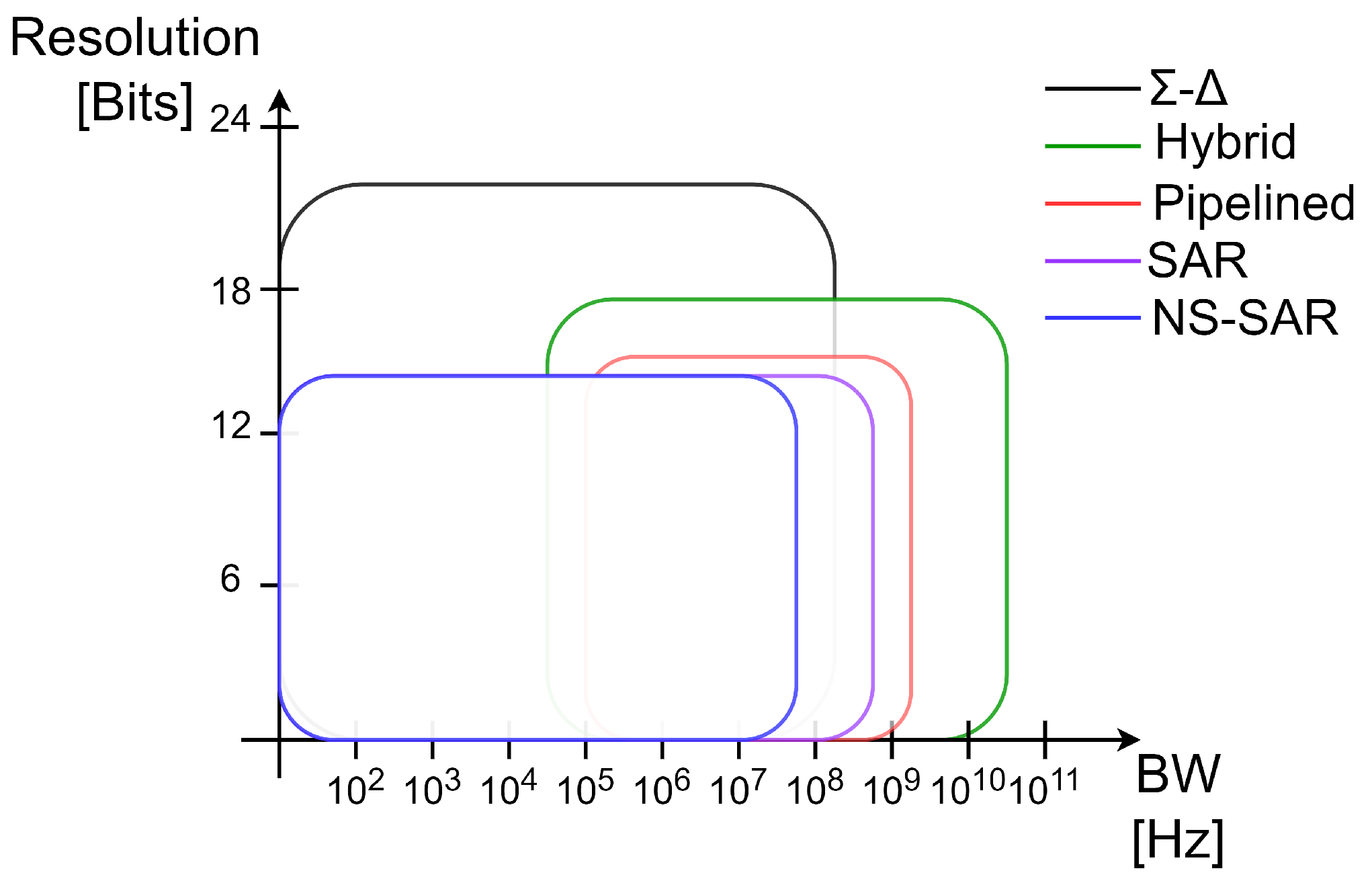
Figure 2.
Power consumption comparison in conventional A/D converter architectures and in NS-SARs.
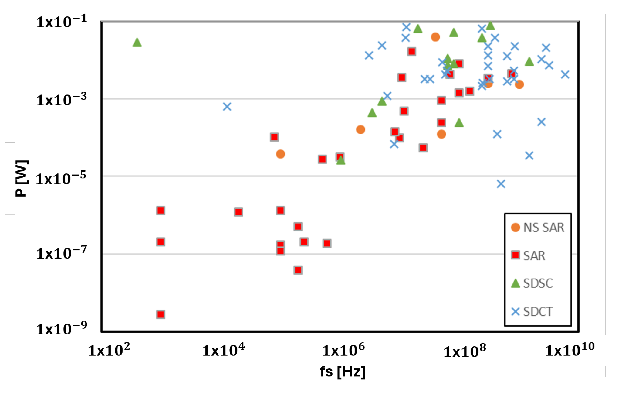
Figure 3.
Traditional SAR ADC schematics.
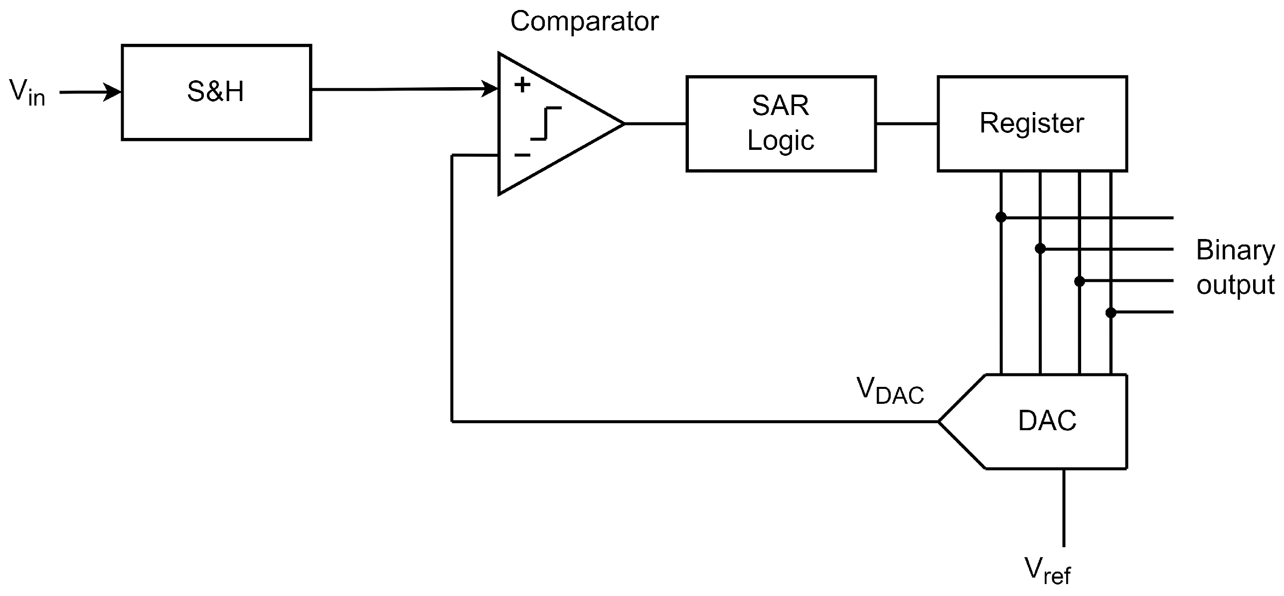
Figure 4.
A 4-bit single-ended CDAC (a) and conventional comparator (b).

Figure 5.
Capacitive voltage divider in the first conversion cycle (a) and comparator-based switched amplifier (b).
Figure 5.
Capacitive voltage divider in the first conversion cycle (a) and comparator-based switched amplifier (b).
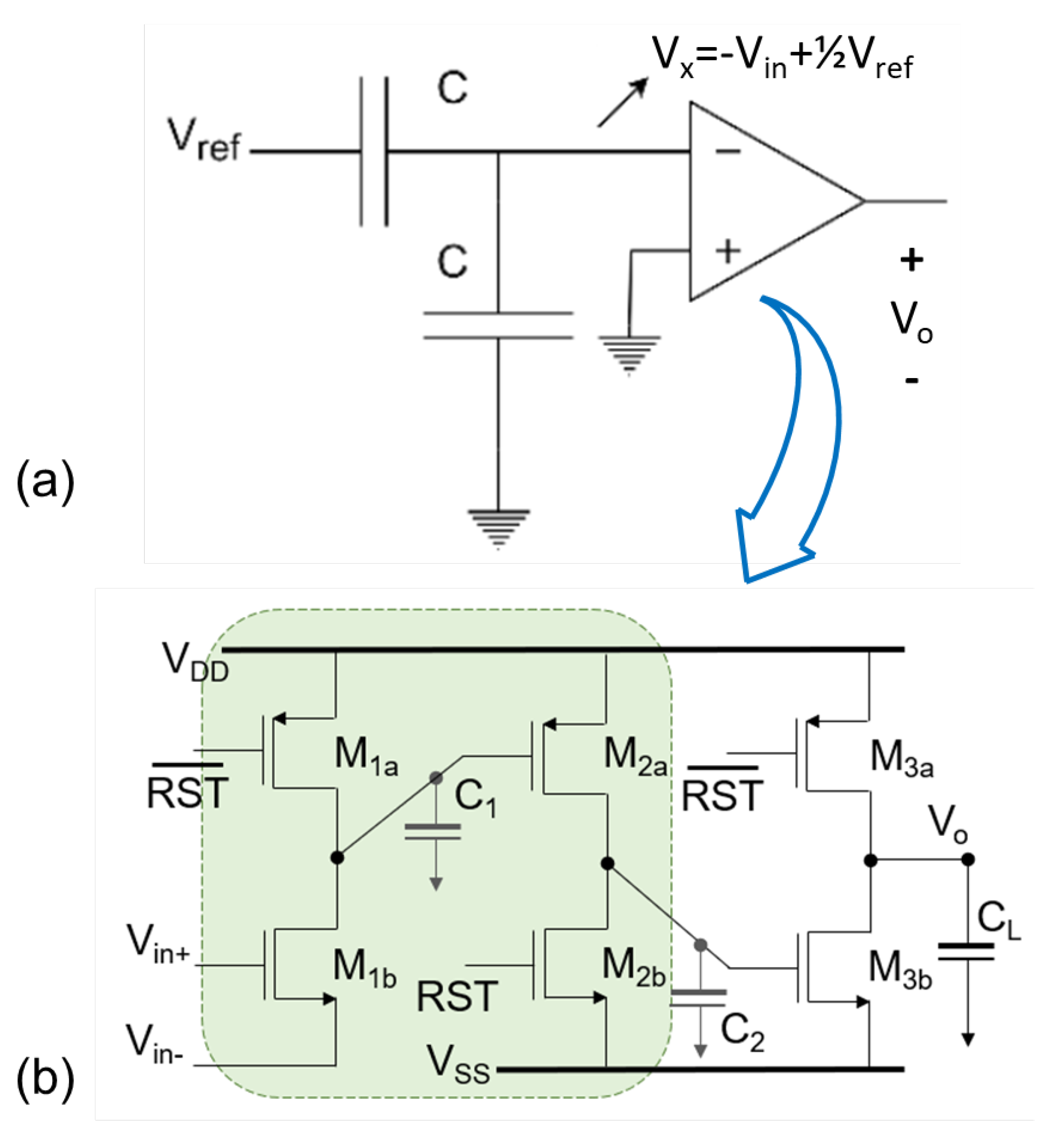
Figure 6.
Four-bit CDAC sampling (a) top plate, (b) bottom plate, and (c) dynamic comparator.
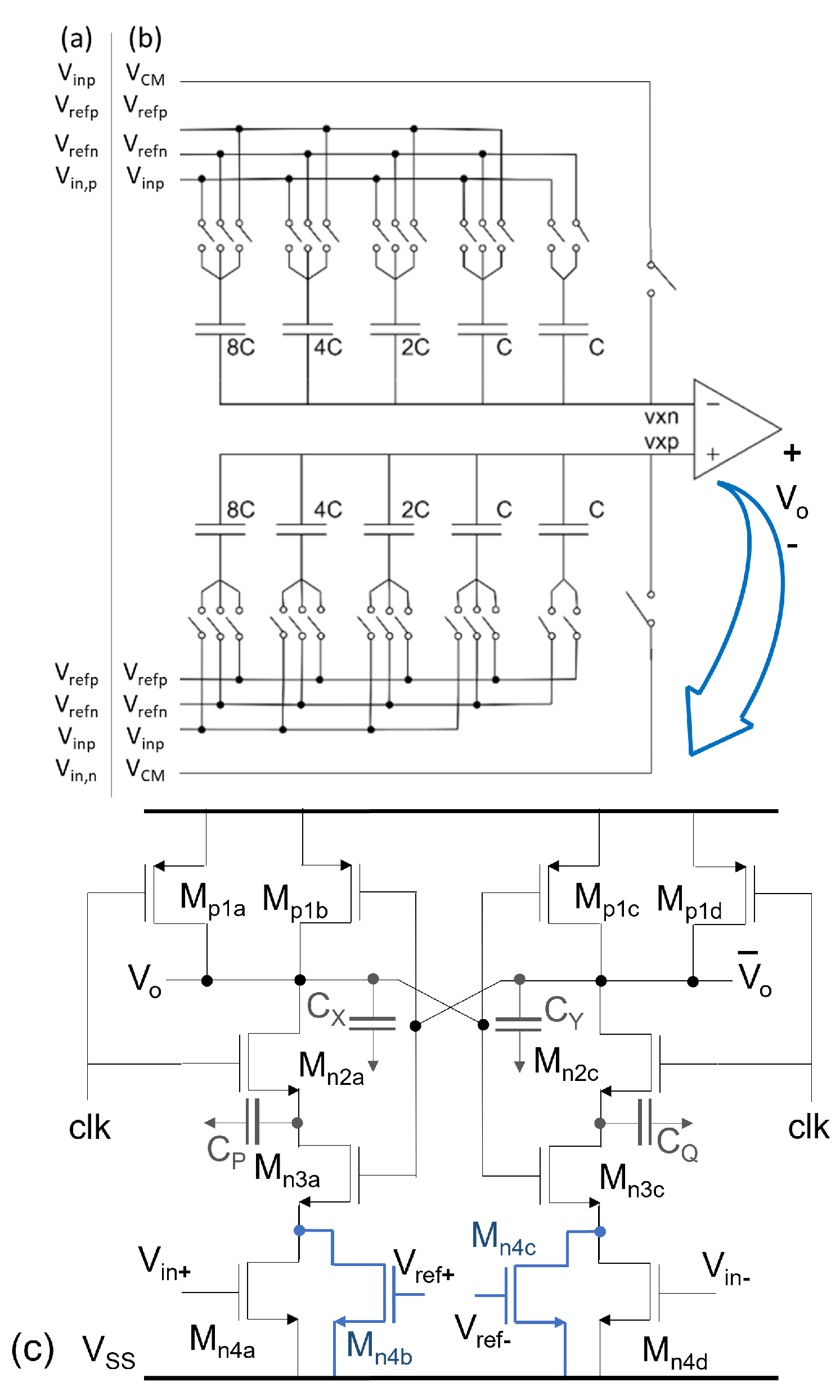
Figure 7.
Full differential binary search algorithm in 4-bit CDAC.
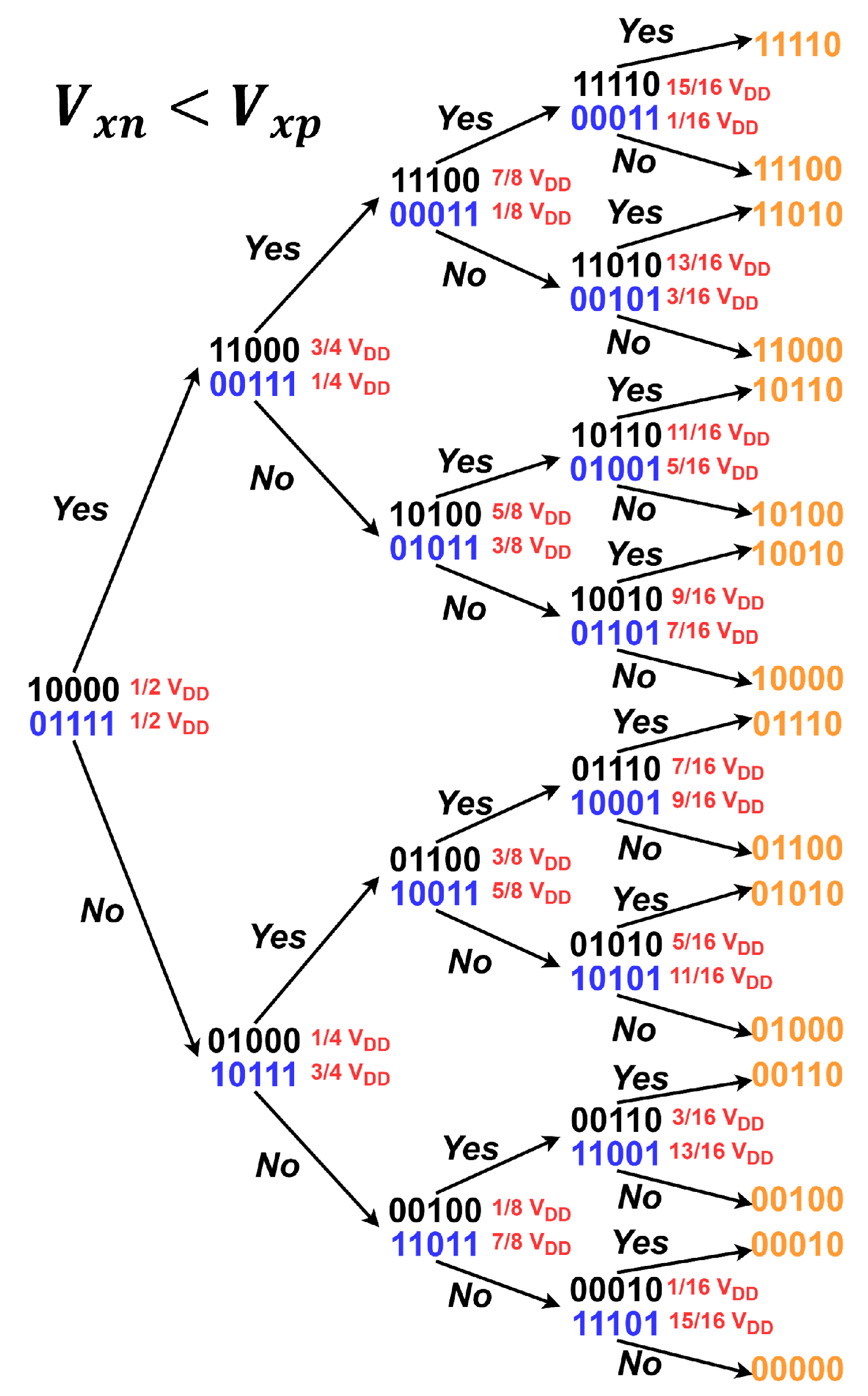
Figure 8.
Differential conversion process of a 10-bit SAR ADC.
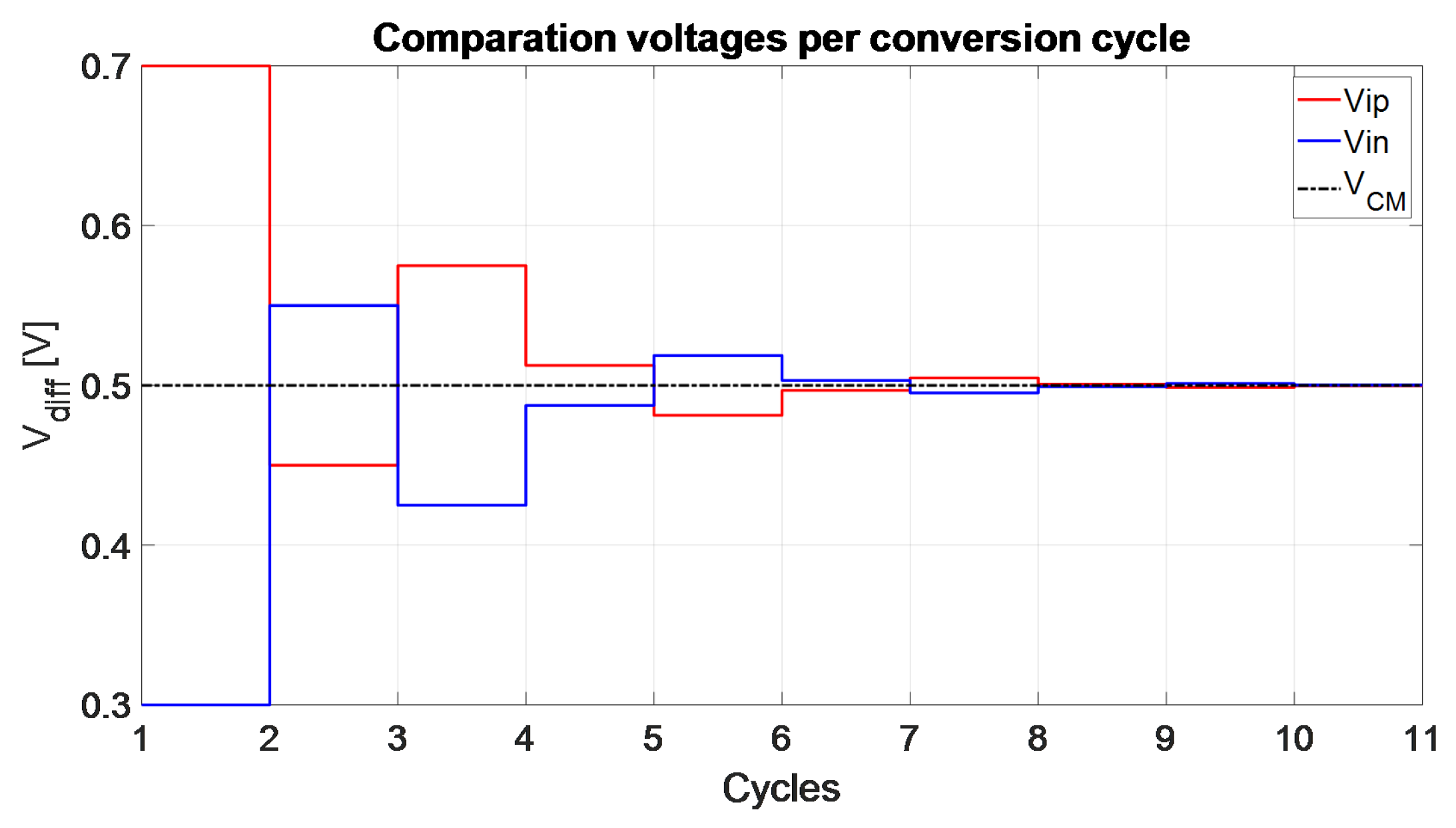
Figure 9.
Error Feedback NS SAR schematics.
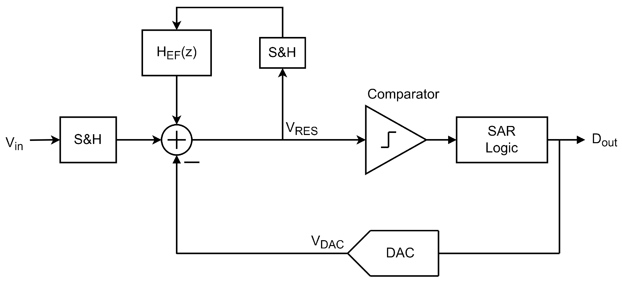
Figure 10.
Cascade Integrator Feed-Forward NS SAR schematics.

Figure 11.
EF NS SAR ADC block diagram.

Figure 12.
CIFF NS SAR ADC block diagram.
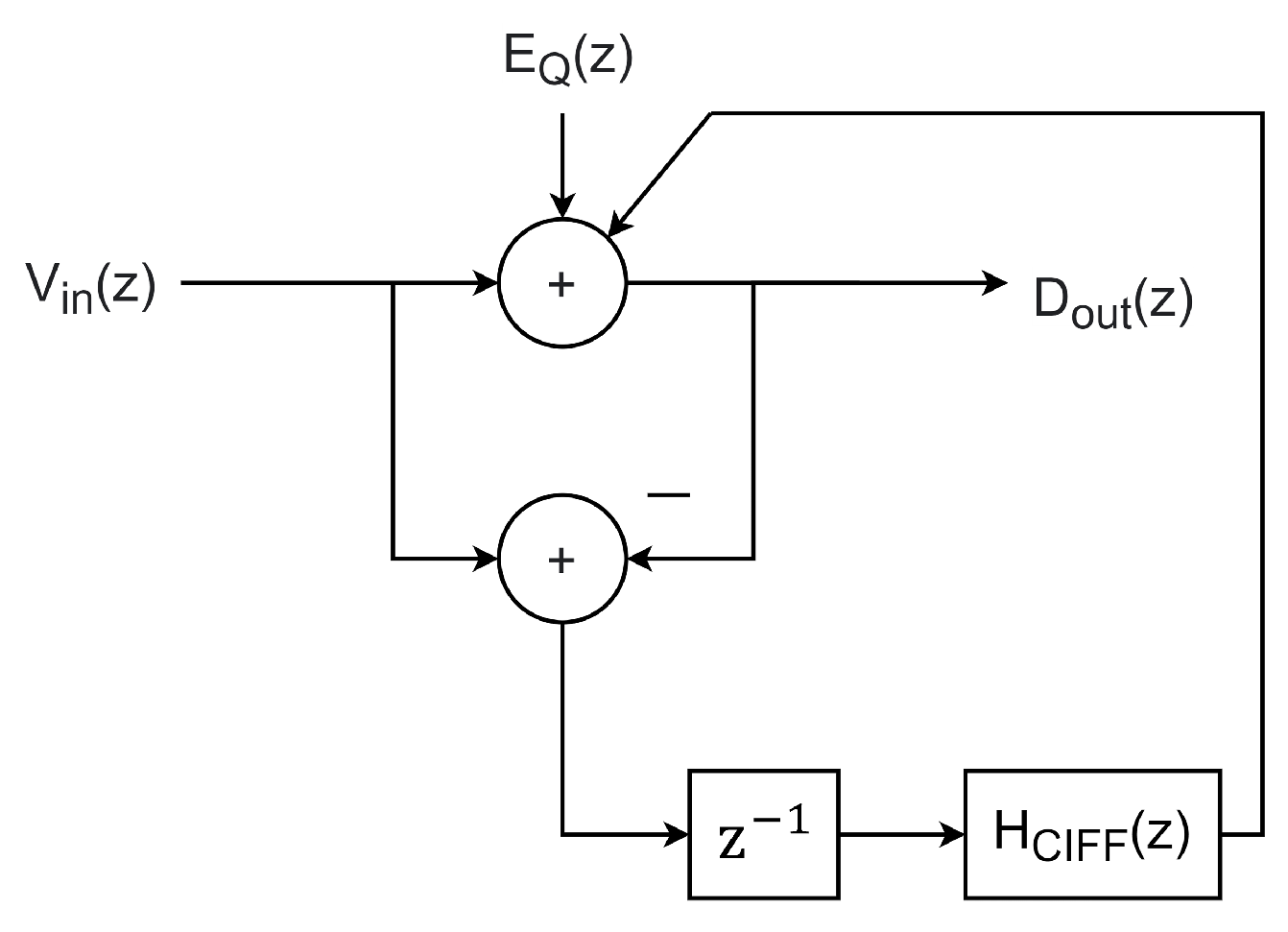
Figure 13.
Representation of the value of in a unit circle.
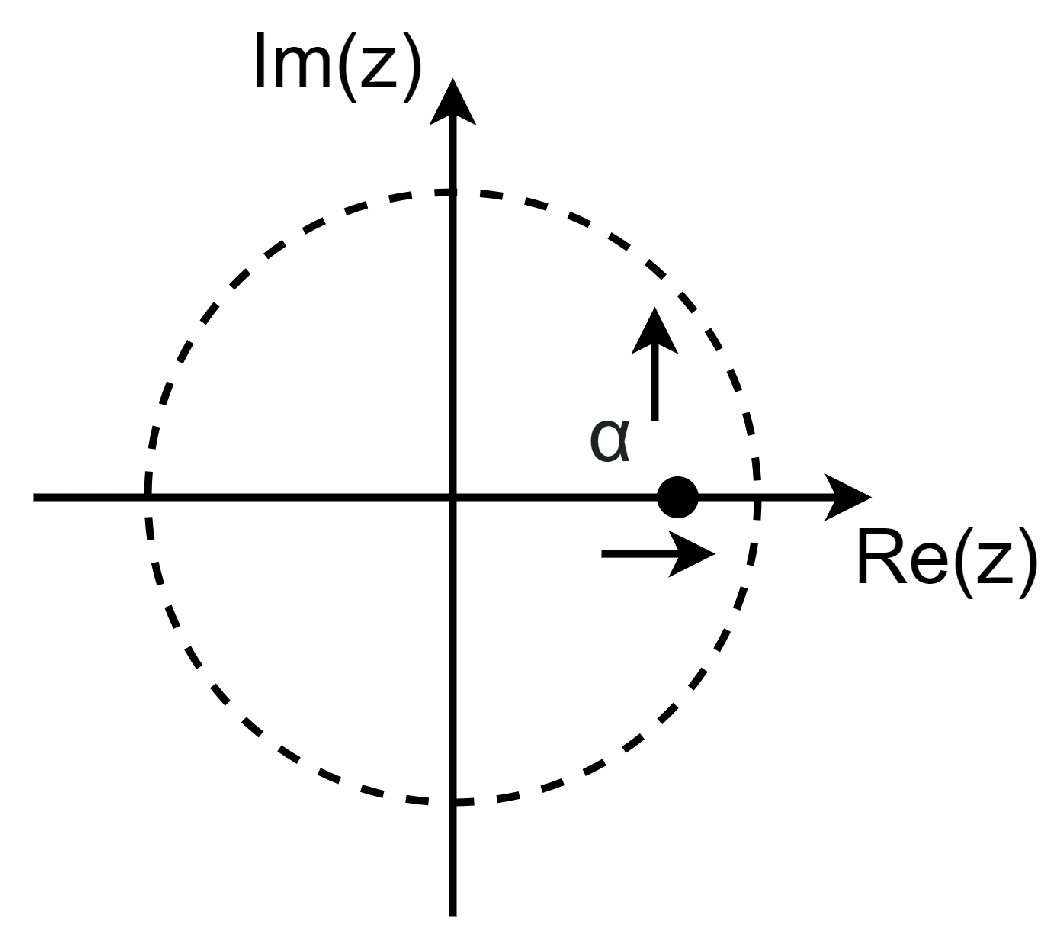
Figure 14.
Active SC third-order implementation [21].
Figure 14.
Active SC third-order implementation [21].
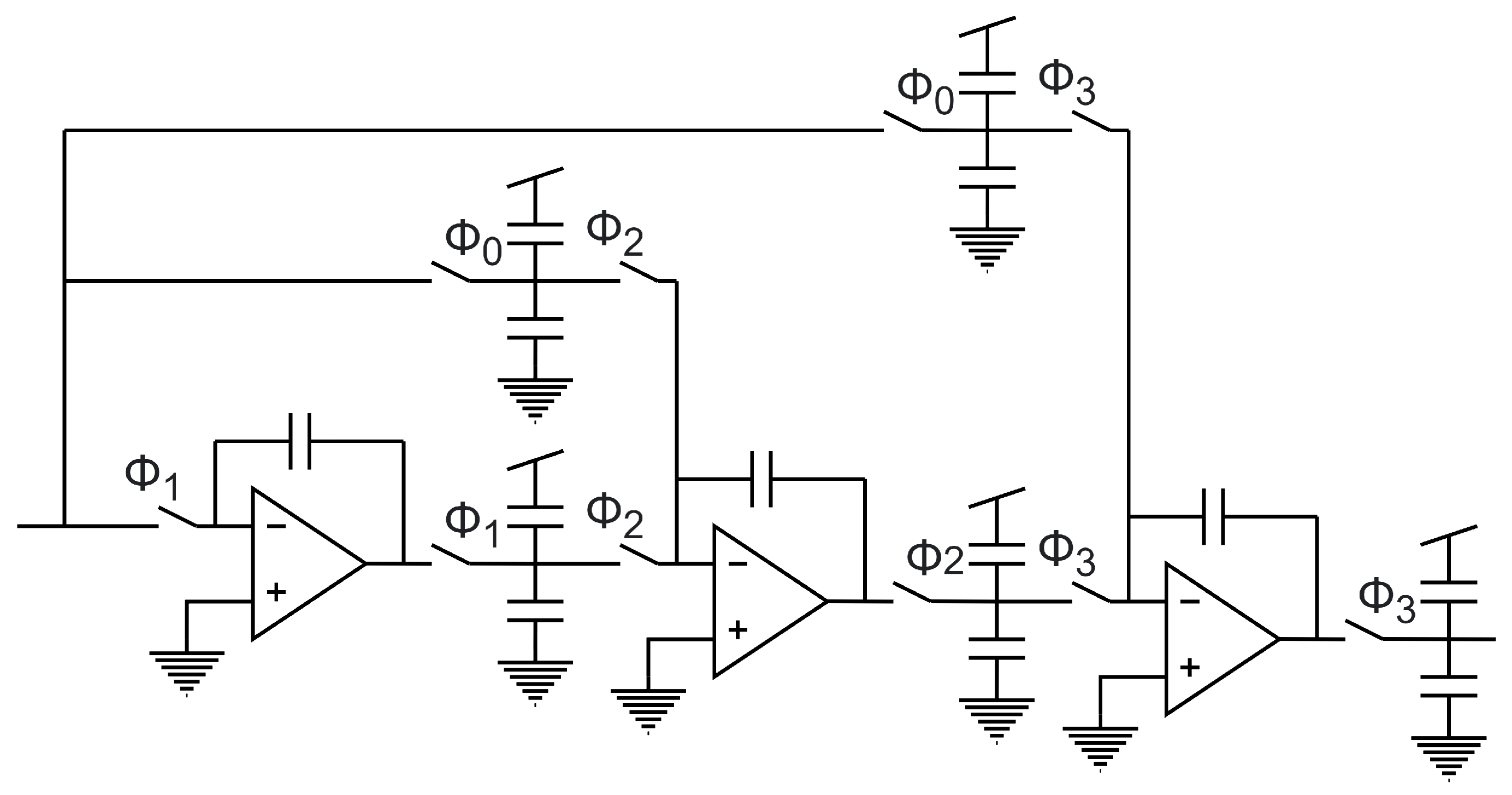
Figure 15.
DA-based multi-input comparator.
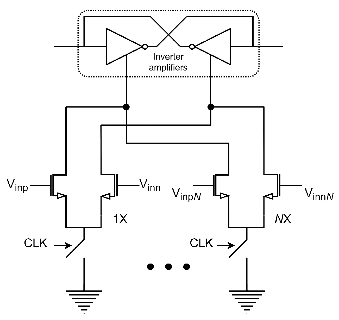
Figure 16.
Capacitor stacking to double voltage.
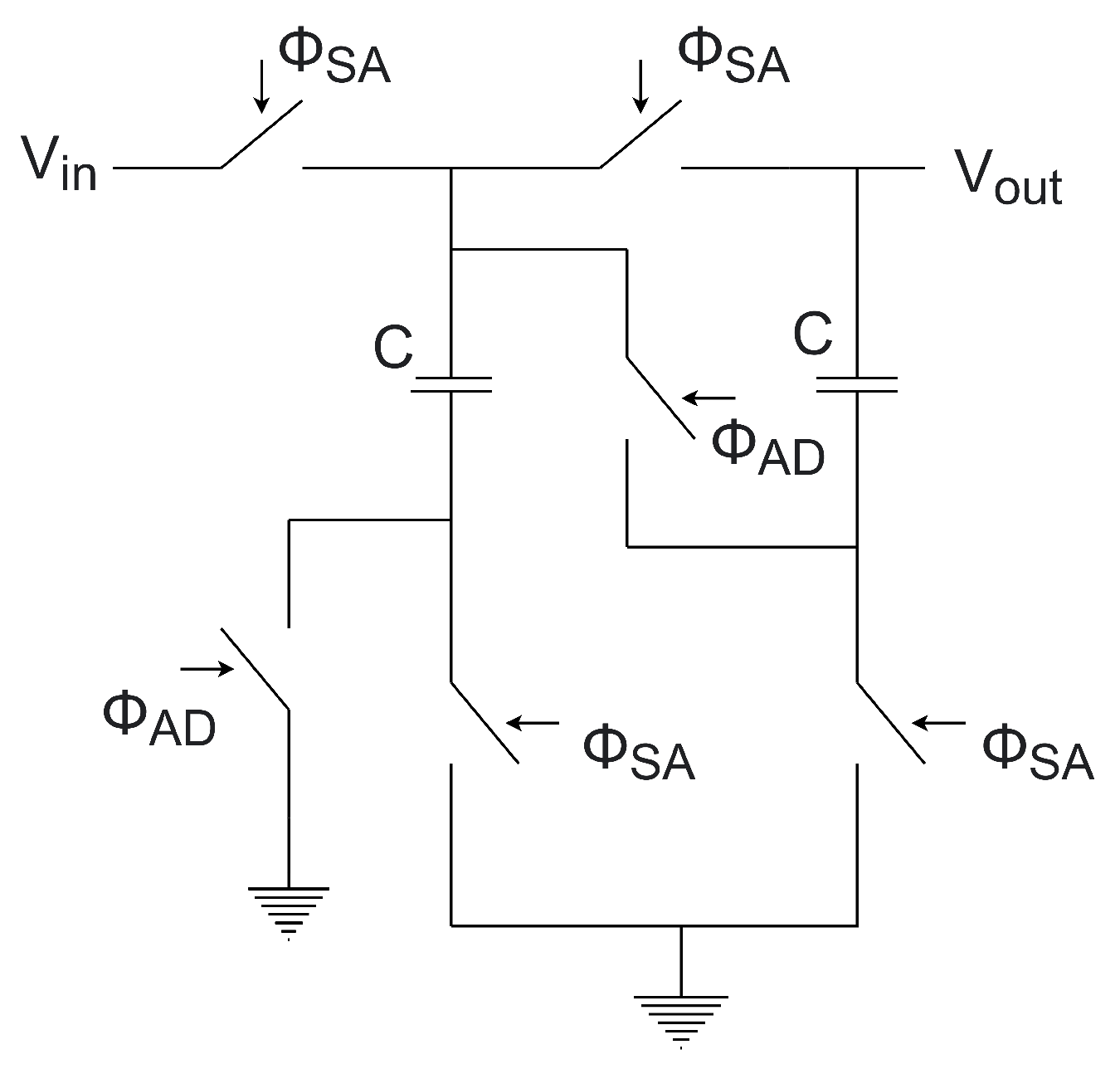
Figure 17.
PSD without noise shaping.
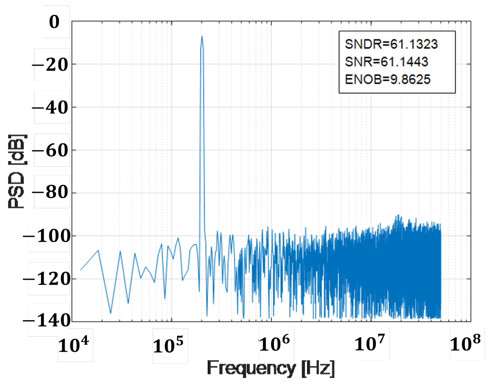
Figure 18.
PSD with first-order noise shaping.
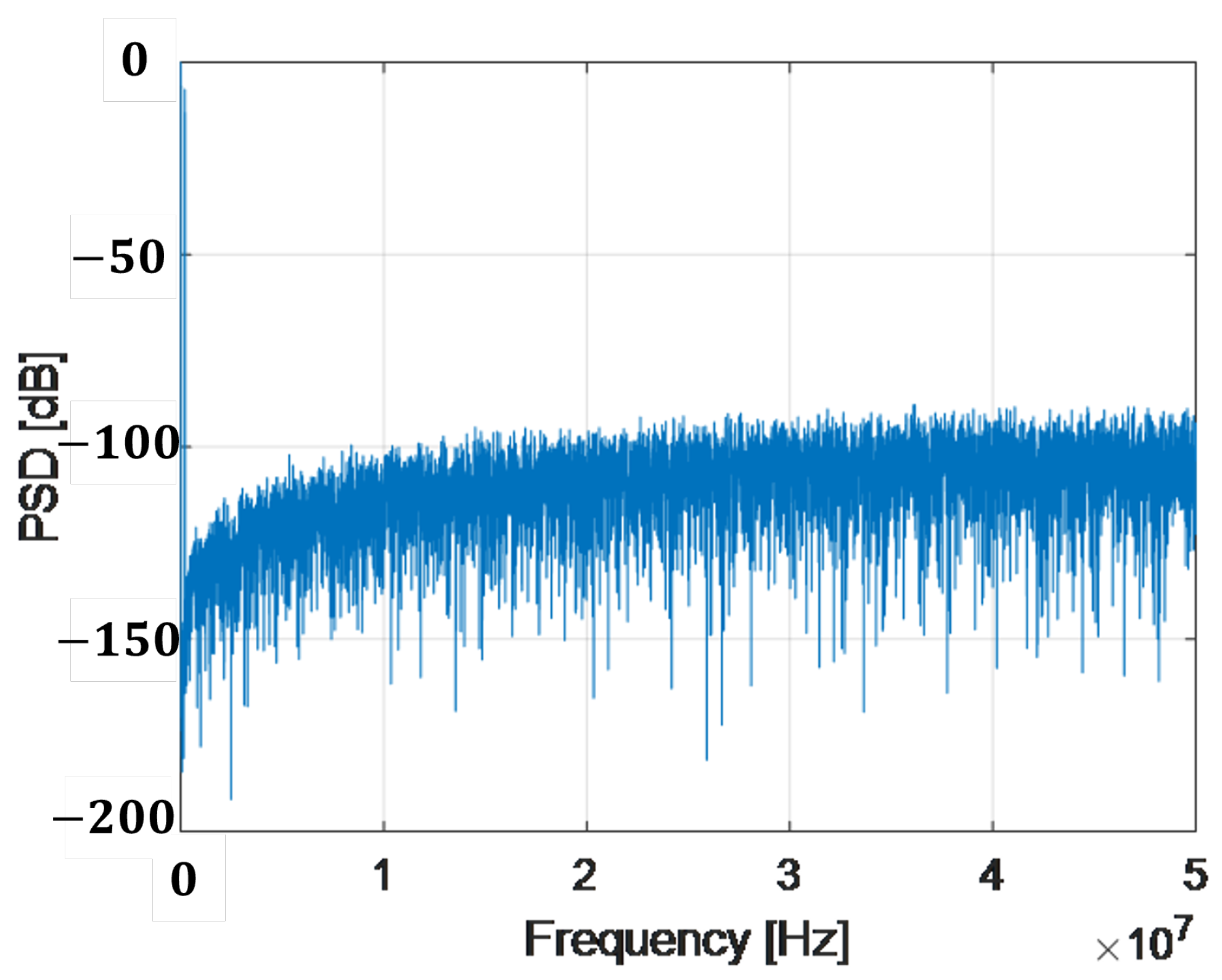
Figure 19.
Semilog chart of PSD with first-order noise shaping and 20 dB/dec slope.

Figure 20.
PSD with second-order noise shaping.
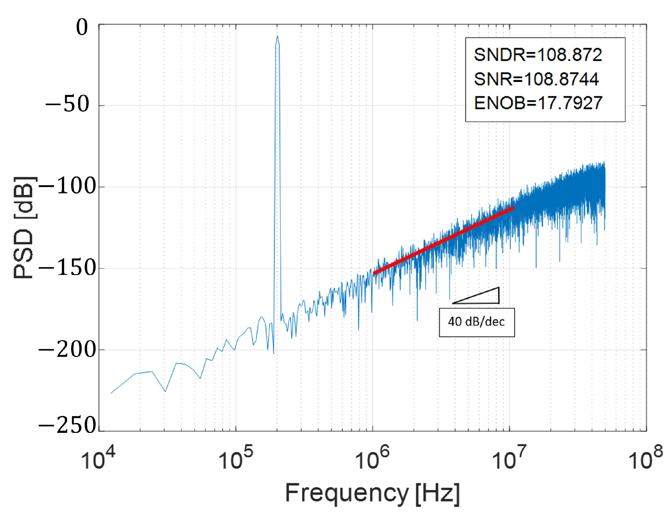
Figure 21.
PSD with third-order noise shaping.
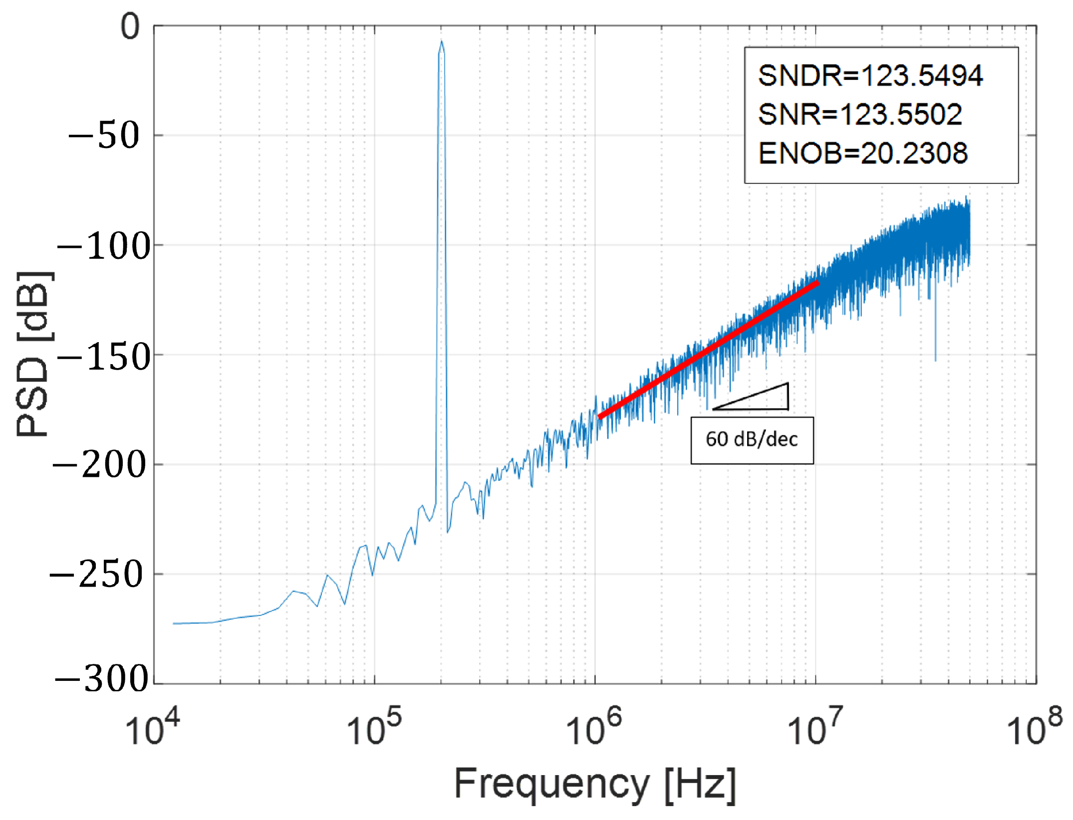
Figure 22.
Linear and non-linear characteristics in A/D conversion.
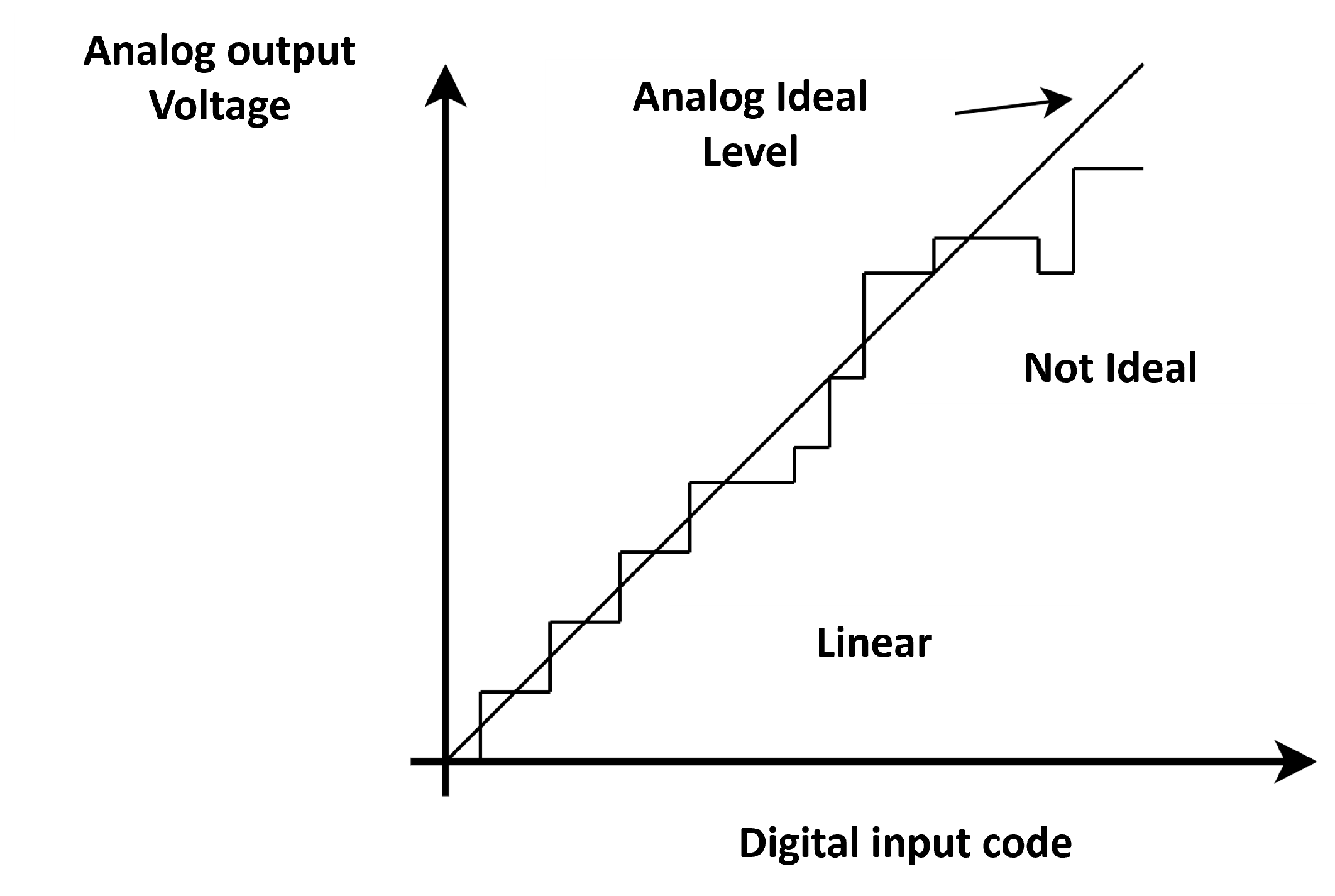
Figure 23.
PSD with one mismatch in a first-order implementation EF.
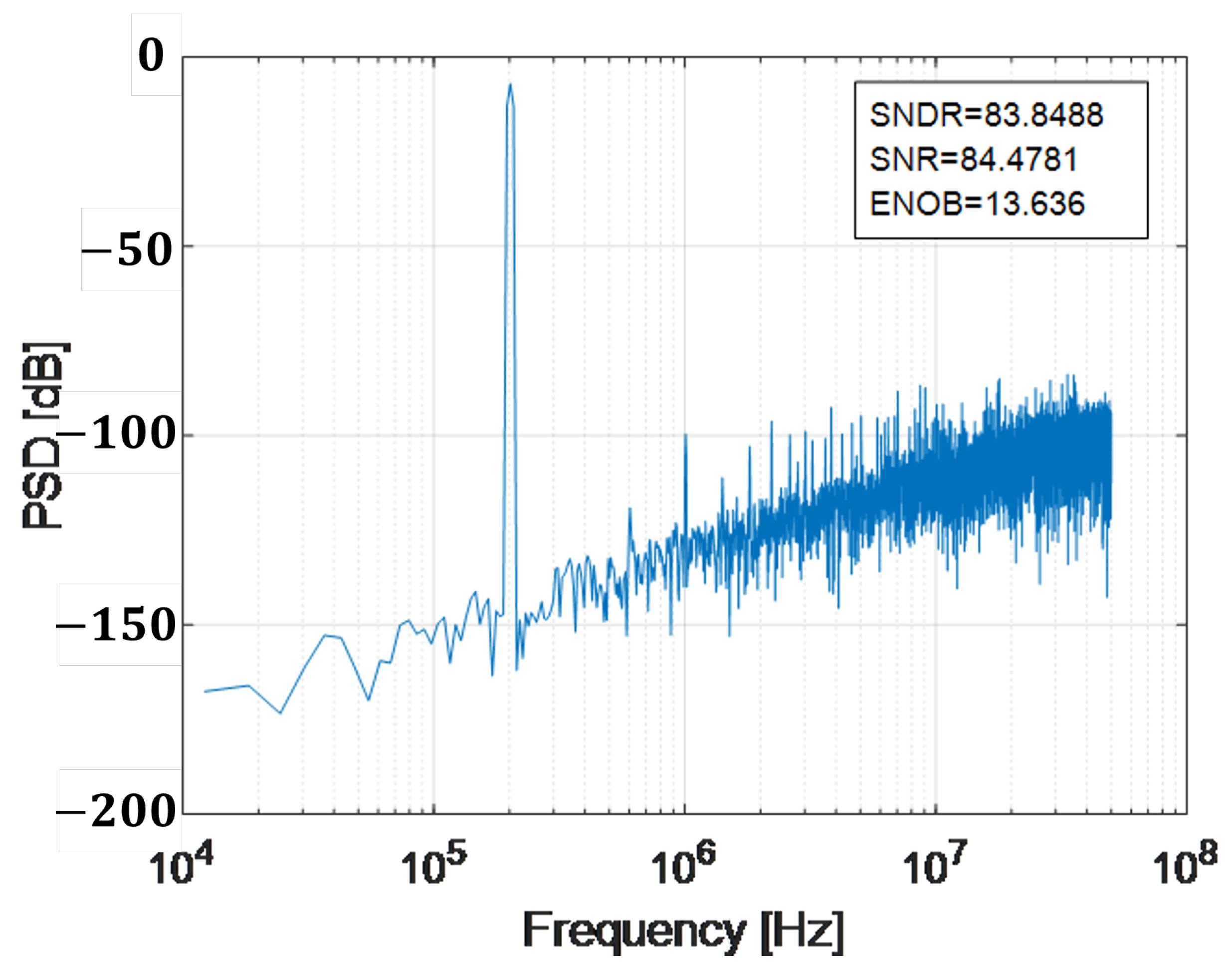
Figure 24.
First-order MES. Sampling phase and LSBs reset stage.
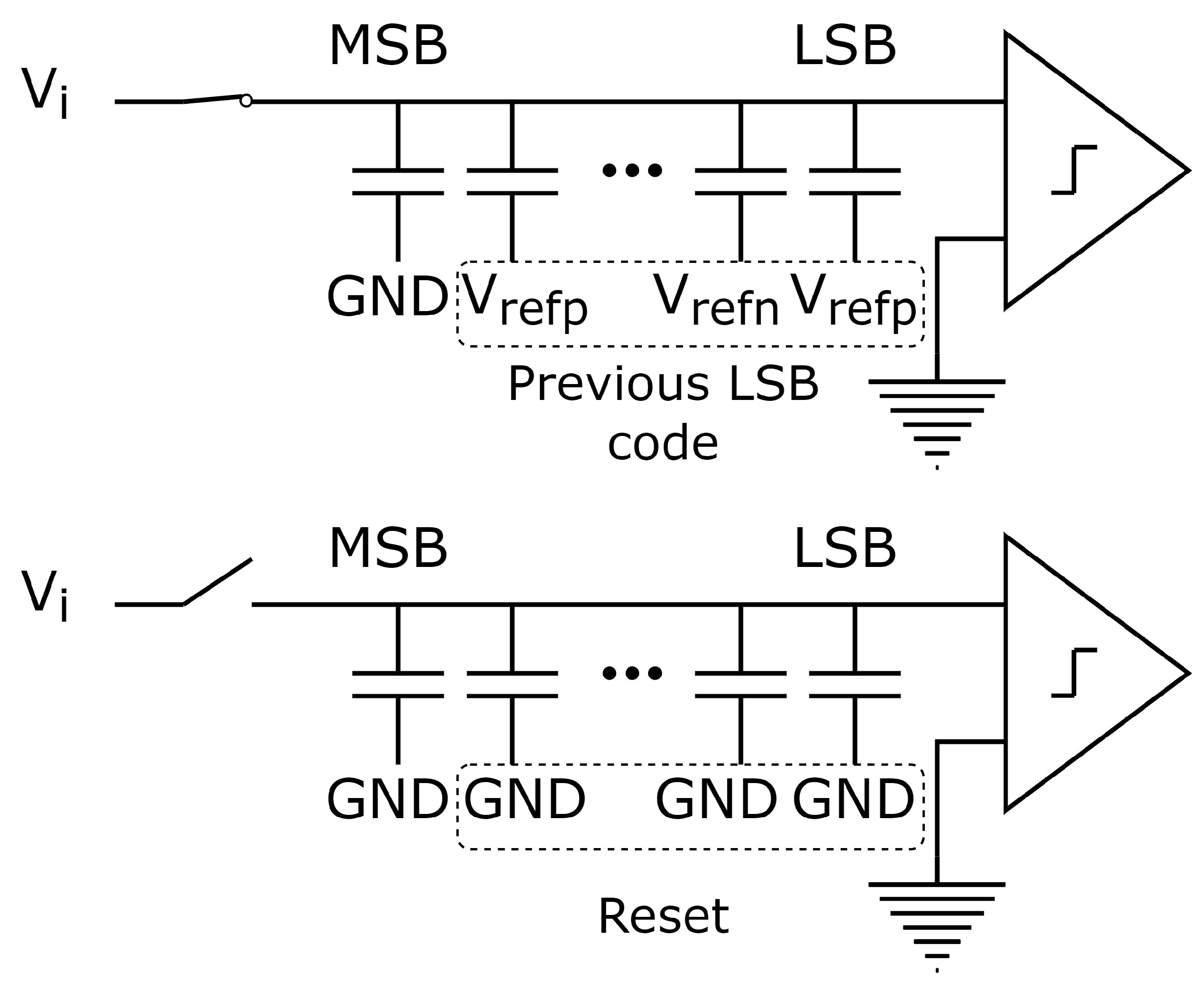
Figure 25.
DEM process.
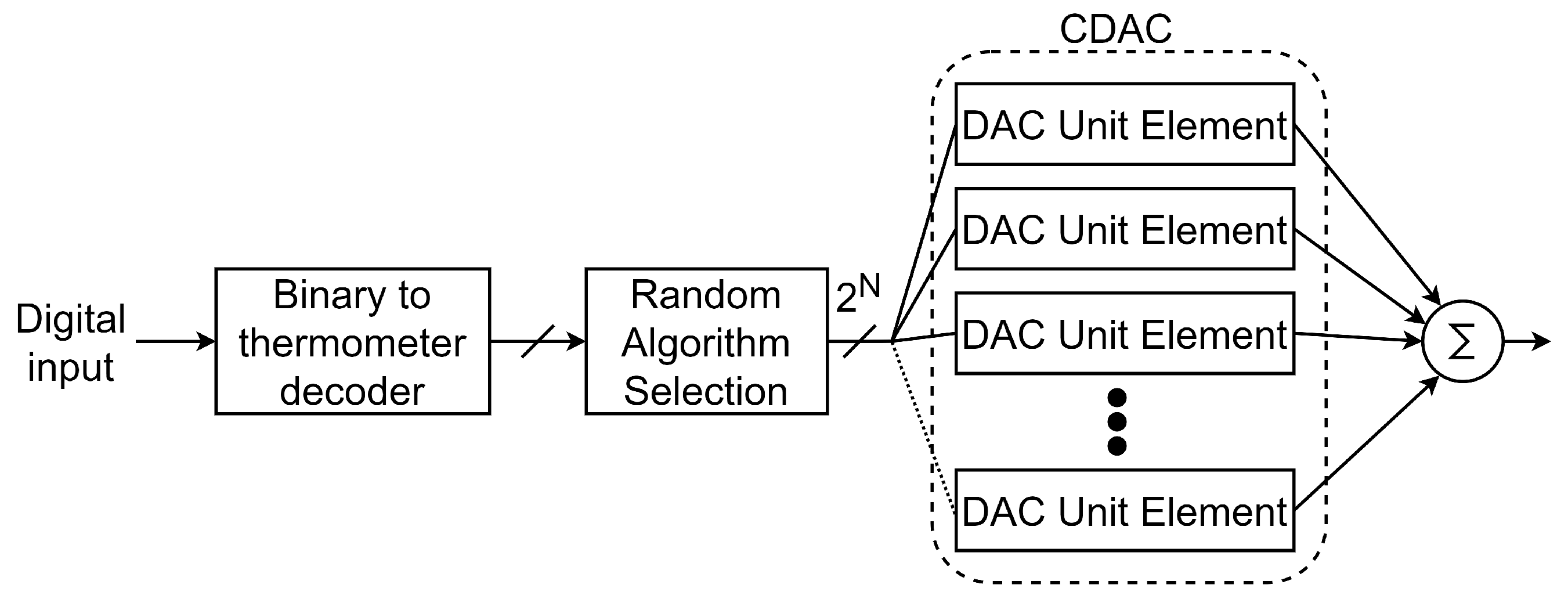
Figure 26.
Unit element selection using DWA algorithm.
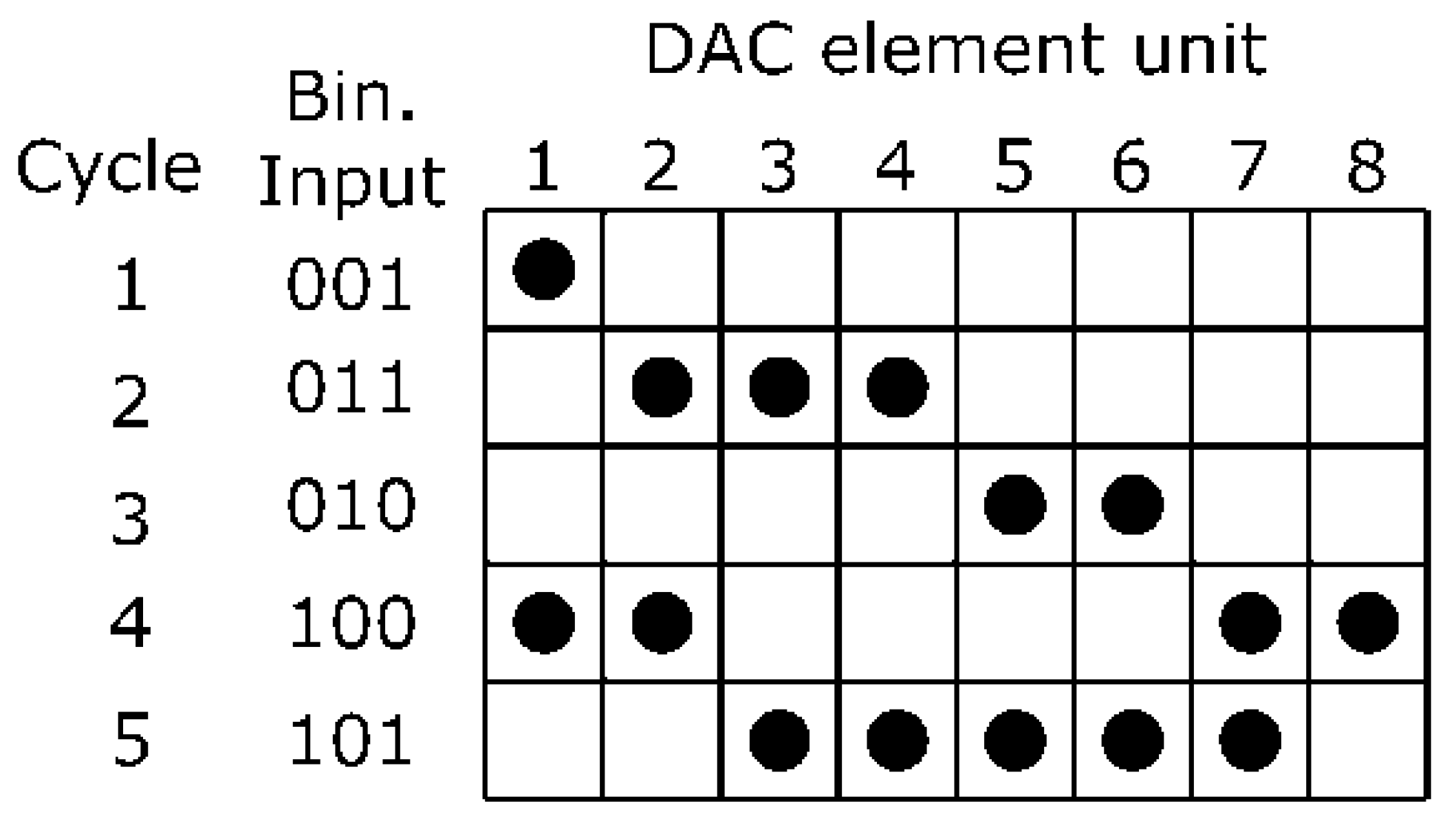
Figure 27.
Block diagram of a NS SAR with the different error sources. The block L(z) that is added to the error, (z), is intended to perform a noise shaping.
Figure 27.
Block diagram of a NS SAR with the different error sources. The block L(z) that is added to the error, (z), is intended to perform a noise shaping.
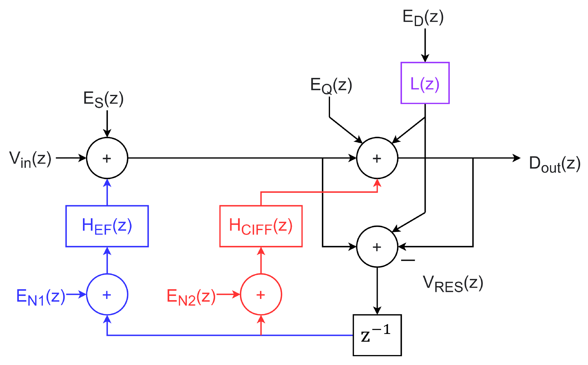
Figure 28.
StrongArm Latch.
Figure 29.
Double Tail Comparator.
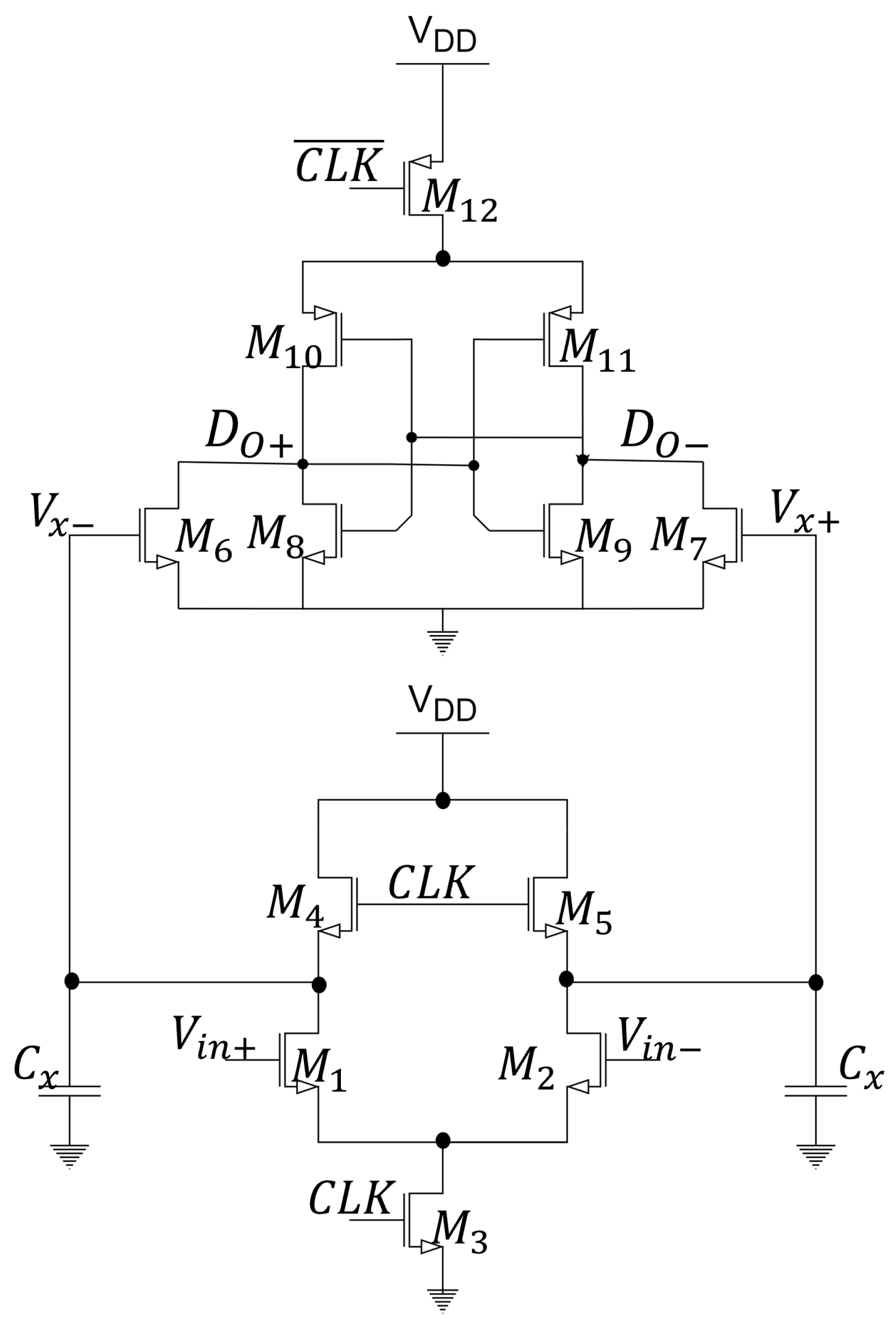
Figure 30.
(a) Dynamic two-stage comparator and (b) dynamic bias comparator.
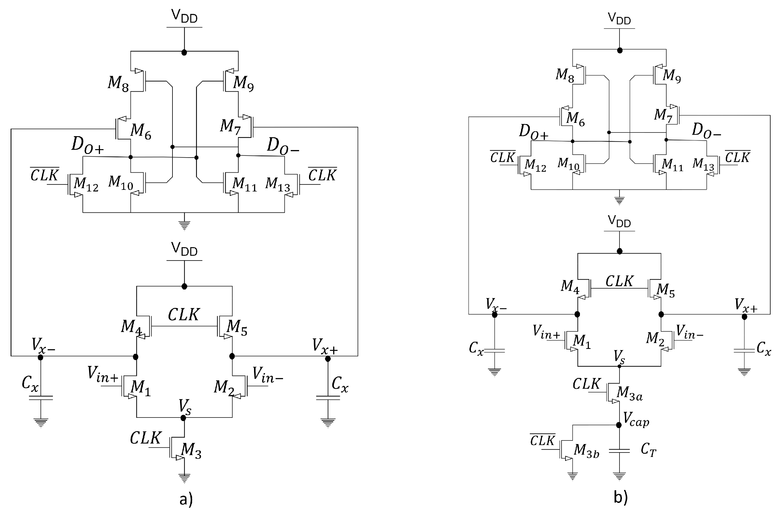
Figure 31.
(a) Floating inverter amplifier and (b) SA latch.

Figure 32.
Low-power dynamic comparator.
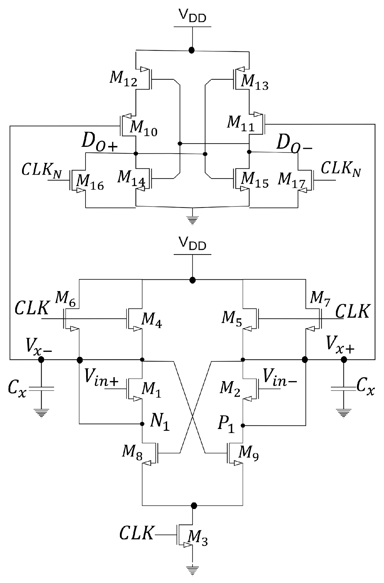
Figure 33.
NS SAR MASH 2-2 fourth-order without OTA [71].
Figure 33.
NS SAR MASH 2-2 fourth-order without OTA [71].
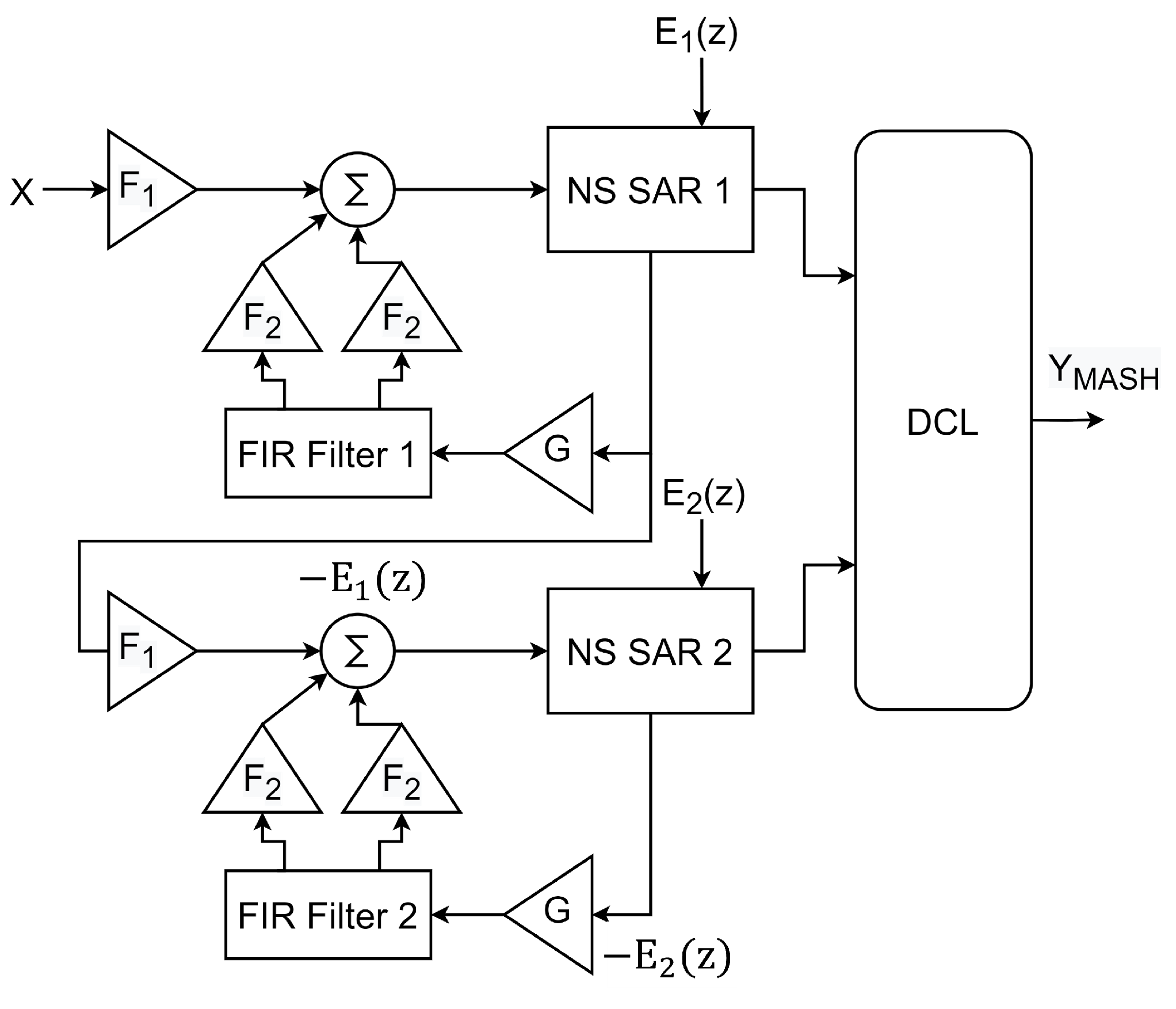
Table 2.
Comparative performance of cascaded/hybrid implementations.
| Specification | Lu 2020 [31] | Wang 2021 [32] | Zhang 2022 [33] | Wang 2022 [34] | Fu 2022 [35] |
|---|---|---|---|---|---|
| Filter | Cascade-EF | EF-CIFF | EF-CIFF | EF-CRFF | CRFF |
| Process | 28 nm | 65 nm | 130 nm | 65 nm | 180 nm |
| Order | 4 | 3 | 3 | 4 | 2 |
| Supply | 1 V | 1.1 V | 1.2 V | 2 V | 1.8 V |
| Bits | 10 | 10 | 8 | 10 | 10 |
| BW | 100 kHz | 625 kHz | 125 kHz | 500 kHz | 1 MHz |
| OSR | 10 | 8 | 8 | 5 | - |
| SNDR | 87.6 dB | 84.8 dB | 79.5 dB | 84.1 dB | 89.4 dB |
| Power | 120 µW | 119 µW | 96 µW | 134 µW | 880 µW |
| FoMs | 176.8 dB | 182 dB | 170.7 dB | 182.4 dB | 187.3 |
Table 3.
Challenges and solutions in the design of NS SAR.
| Problem | Solutions | Techniques |
|---|---|---|
| Mismatch in DAC | Increment in CDAC area | · Larger DAC unit elements |
| Digital calibration | · Foreground · Background | |
| Digital Mismatch Shaping-Dynamic Element Matching (DEM) | · Data Weighted Averaging (DWA) · Segmented DEM | |
| Mismatch Error Shaping (MES) | · Preset of LSBs | |
| kT/C and flicker noise + offset | Switches and amplifiers designs | · Clock Boosting · Bootstrapping · Buffer design · Chopper modulation |
Table 4.
Comparative mismatch correction techniques.
| Reference | Calibration Technique | SFDR [dB] |
|---|---|---|
| Li 2018 [17] | Background LMS | 89 |
| Zhuang 2019 [24] | Background LMS | 90 |
| Jie 2020 [47] | LUT Foreground | 102.8 |
| Liu 2021 [39] | Foreground | 104.4 |
| Wang 2021 [32] | Foreground LMS | 103 |
| Liu 2019 [42] | MES | 122* |
| Yang 2022 [40] | MES | 104.5 |
| Li 2021 [41] | MES | 98 |
| Shen 2022 [43] | MES | 103 |
| Li 2022 [16] | MES | 98 |
| Obata 2016 [21] | DEM + Dither | 112 |
| Miyahara 2017 [48] | Binary mode DEM | 84.3 |
| CC Liu 2017 [49] | DWA | 92.2 |
| Zhang 2020 [50] | DWA | 97.34 |
| Zhang 2021 [27] | DWA | 92.9 |
| Shu 2016 [20] | MES + DWA | 105.1 |
| Liu 2020 [23] | MES + DWA | 102.2 |
| Hasebe 2022 [46] | MES + DWA | 108.5 |
Disclaimer/Publisher’s Note: The statements, opinions and data contained in all publications are solely those of the individual author(s) and contributor(s) and not of MDPI and/or the editor(s). MDPI and/or the editor(s) disclaim responsibility for any injury to people or property resulting from any ideas, methods, instructions or products referred to in the content. |
© 2024 by the authors. Licensee MDPI, Basel, Switzerland. This article is an open access article distributed under the terms and conditions of the Creative Commons Attribution (CC BY) license (https://creativecommons.org/licenses/by/4.0/).
Share and Cite
MDPI and ACS Style
Arzate-Palma, V.H.; Rivera-Orozco, D.G.; Molina Salgado, G.; Sandoval-Ibarra, F. A Review on Fundamentals of Noise-Shaping SAR ADCs and Design Considerations. Chips 2024, 3, 153-181. https://doi.org/10.3390/chips3020007
AMA Style
Arzate-Palma VH, Rivera-Orozco DG, Molina Salgado G, Sandoval-Ibarra F. A Review on Fundamentals of Noise-Shaping SAR ADCs and Design Considerations. Chips. 2024; 3(2):153-181. https://doi.org/10.3390/chips3020007
Chicago/Turabian StyleArzate-Palma, Victor H., David G. Rivera-Orozco, Gerardo Molina Salgado, and Federico Sandoval-Ibarra. 2024. "A Review on Fundamentals of Noise-Shaping SAR ADCs and Design Considerations" Chips 3, no. 2: 153-181. https://doi.org/10.3390/chips3020007