Article

Possibility of Fabricating Anisotropic Conductive Film with a Line-and-Space-Like Pattern by Stick-Slip Accompanying Abrasion

Faculty of Engineering, Gifu University, 1-1 Yanagido, Gifu-shi, Gifu 501-1193, Japan
*
Author to whom correspondence should be addressed.
J. Manuf. Mater. Process. 2019, 3(3), 60; https://doi.org/10.3390/jmmp3030060
Submission received: 28 June 2019 / Revised: 12 July 2019 / Accepted: 22 July 2019 / Published: 23 July 2019

Abstract

:
The development of an anisotropic conductive film was attempted using original microfabrication (stick-slip (SS) processing) involving SS accompanying abrasion. During SS processing, the film surface was periodically scraped with a razor. For a metal-deposited polyethylene terephthalate (PET) film (metal/PET film), fine periodic structures (line and space (L/S)-like patterns) were formed on its surface because the metal layer was periodically scraped. This result proved that SS processing can be applied not only to polymers but also to metals. Moreover, the line interval of an SS-processed metal/PET film shortened as the contact force decreased, and the depth of the line became shallower in proportion to the line interval. In addition, SS-processed copper/PET (Cu/PET) film did not conduct electricity in the direction perpendicular to the Cu line; however, it conducted electricity in the direction parallel. Thus, this study shows the possibility of using SS processing for fabricating an anisotropic conductive film.

1. Introduction

An original, simple, and low-cost microfabrication method (stick-slip (SS) processing) was developed by the authors [1]. This process utilizes SS [2,3] accompanying abrasion [4,5,6], wherein the sample surface is periodically scraped. The films produced using this technique have a fine periodic structure with a pitch of several hundred nanometers to several tens of micrometers on their surfaces. We already reported several applications involving fabrication using this technique. And that applications are a film with anisotropic wettability and fiber with wavy periodic structure on its surface [7,8]. In the past, SS processing has only been used for polymer films (insulators that do not conduct electricity), though SS processing can in principle also be applied to any materials, including metals, as long as friction occurs under the condition that the static friction coefficient is larger than the kinetic friction coefficient. However, the current SS processing device can only process films and fibers. If SS processing were to be applied to metal films, it would likely break during the process.
Therefore, in this study, we attempted to perform SS processing of polymer films with surface metal layers. If the metal layer can be periodically scraped off, it can be expected to become an anisotropic conductive film having line-and-space (L/S)-like patterns (width of wiring and intervals in wiring) consisting of metal layers (lines) and grooves (spaces). The anisotropic conductive film will not conduct electricity in the direction perpendicular to the metal line (parallel to the SS processing direction), though it will conduct electricity in the direction parallel to the metal line (perpendicular to the SS processing direction).

2. Materials and Methods

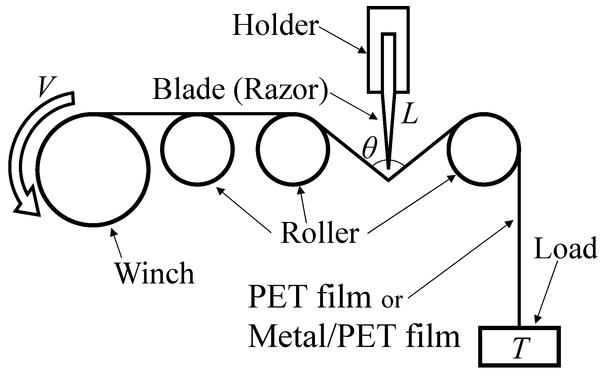
2.1. Materials and Processing Blade

Polyethylene terephthalate (PET) film, commonly used as a base film for conductive films, was selected as the base film. We used a biaxially stretched PET film (FE 2000, Futamura Chemical, Nagoya-shi Aichi, Japan) (thickness: 37 μm, density: 1.38 g/cm3). In addition, we selected copper (Cu), commonly used as a wiring material for electronic circuits, as the material for the metal layer. We also used silver (Ag) for comparison. We used Cu wire (CU-111527, Nilaco, Chuo-ku Tokyo, Japan) and Ag wire (AG-401485, Nilaco, Chuo-ku Tokyo, Japan) for vacuum deposition. Commercially available razors (FAS-10, Feather, Osaka-shi Osaka, Japan) with a sharp tip (tip angle: 15.5°, tip radius: 2.91 μm) were used as blades during SS processing. The raw material of the razors is TE-2 (high-carbon steel). Table 1 shows the Young’s modulus and tensile strength values of the PET film and TE-2 sheet.

2.2. Formation of Metal Layer through Vacuum Deposition

Cu and Ag were deposited on the PET film through vacuum evaporation. A vacuum evaporation apparatus (HUS-5GB, Hitachi, Chiyoda-ku Tokyo, Japan) and tungsten (W) basket (B-110, Nilaco) were used for this purpose. We used a 20 mm wide and 150 mm long rectangular sample film. Its long and short sides were aligned in the machine direction (MD) and transverse direction (TD), respectively. The source-to-substrate distance was 90 mm, and the deposition time was 40 s for Cu and 15 s for Ag. Hereafter, the PET film with deposited metal will be referred to as the metal/PET film. In particular, a Cu-deposited PET film is a Cu/PET film, and an Ag-deposited PET film is an Ag/PET film. Table 2 shows the static and kinetic friction coefficients between the samples (PET or metal/PET film) and the TE-2 sheet. The friction coefficients were measured according to JIS K 7125 (related to ISO 8295, ASTM D 1894).

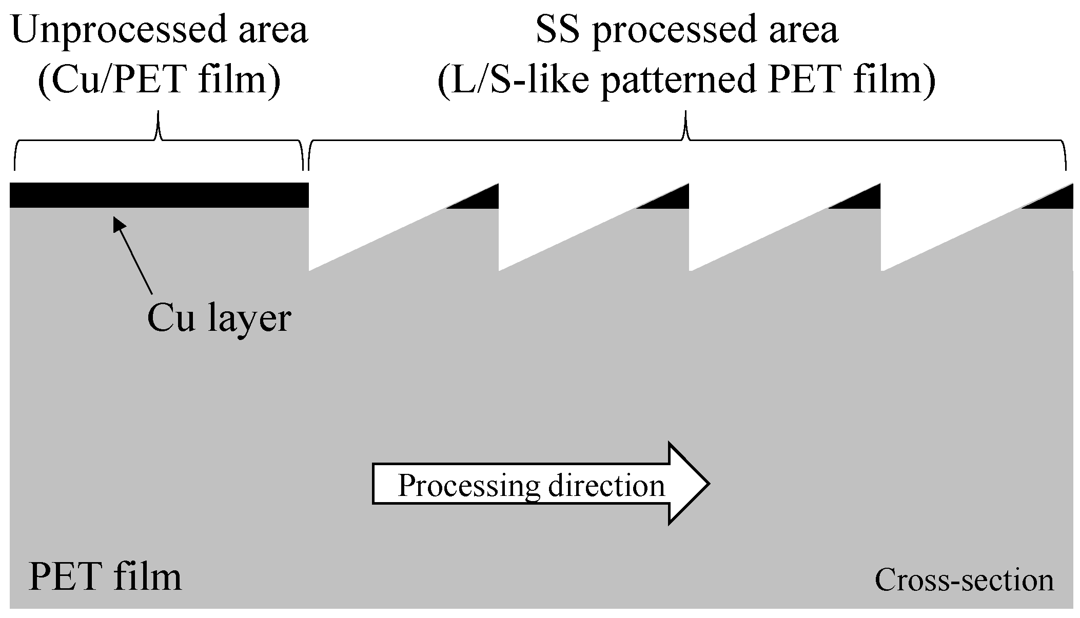
2.3. Formation of L/S-Like Pattern Using Stick-Slip Processing

Figure 1 shows a schematic diagram of the SS processing device. This device consists of a winch for rolling up the sample film, rollers, and a holder for the processing blade. The rotary speed of the winch can be controlled using the control unit; therefore, the processing (rolling-up) speed (V) can be changed. Moreover, the vertical position of the holder can be changed; therefore, the processing angle (θ, the bending angle of the film) can also be changed. We prepared several holders; therefore, the free-end length (L) of the processing blade can be changed by selecting the holder. Furthermore, when one end of the film is held in place by the winch and a weight is hung at its other end, the film becomes taut. Thus, the processing load (T) can be changed by changing the weight. This device can be started after setting the above processing conditions (V, θ, L, T). Consequently, the film was rolled up, and SS accompanying abrasion occurred at the contact area between the sample film and processing blade. A fine periodic structure was then generated on the surface of the film.
In this study, we periodically scraped off the metal layer of the metal/PET film using SS processing to prepare an anisotropic conductive film with an L/S-like pattern on its surface. In addition, we paid attention to the influence of the contact force (W = 2Tcos(θ/2)) between the film and processing blade on the formation of the L/S-like pattern. Therefore, we only adjusted T while the other conditions were unchanged (Table 3). When the metal/PET film underwent SS processing, its metal-coated surface was in contact with the processing blade. In addition, we used a new processing blade for each experiment, since the tip of the processing blade could be damaged during SS processing. Henceforth, the PET film that underwent SS processing will be referred to as the SS-processed film, while the metal/PET film that underwent SS processing will be referred to as the SS-processed metal/PET film (SS-processed Cu/PET film, SS-processed Ag/PET film).

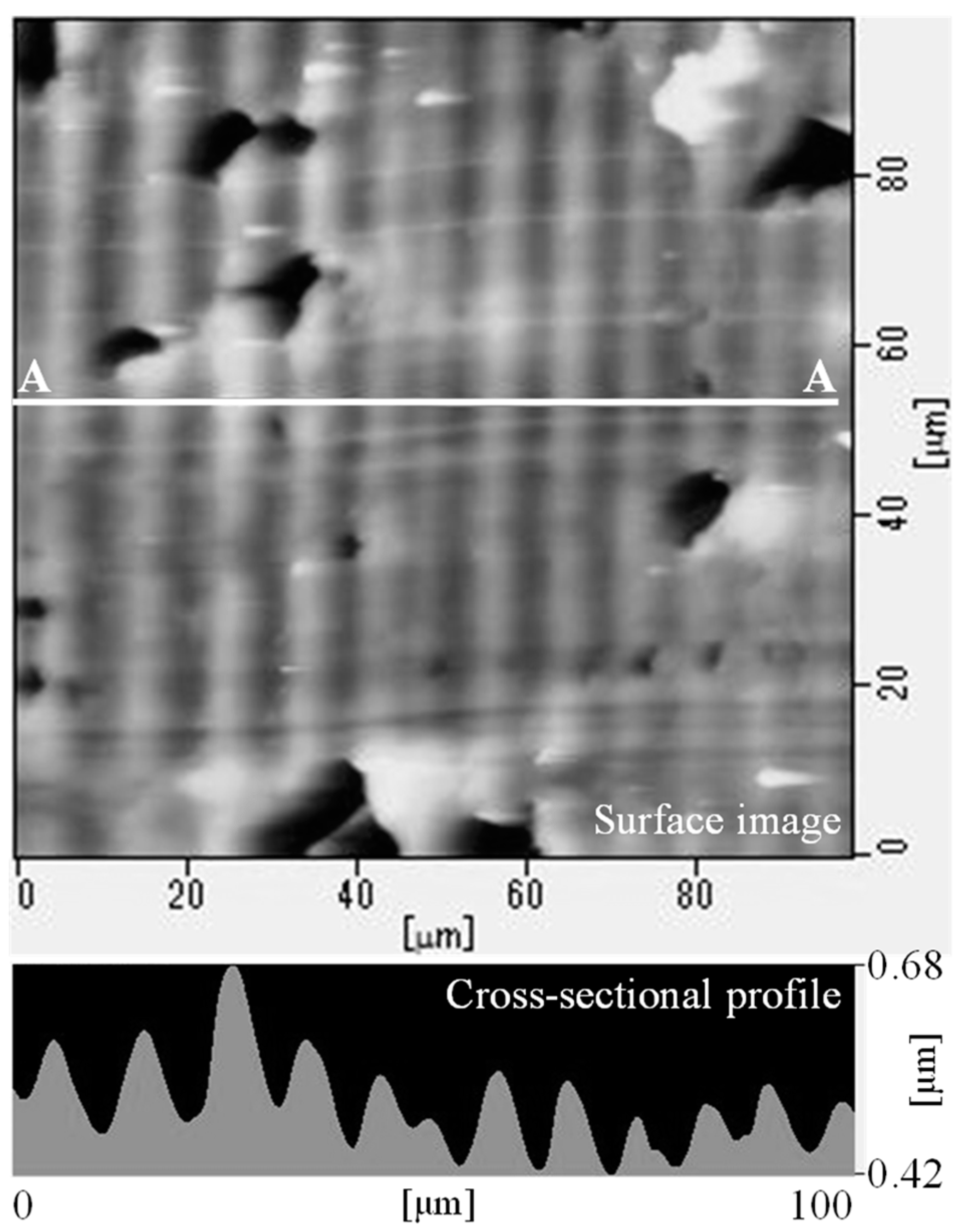
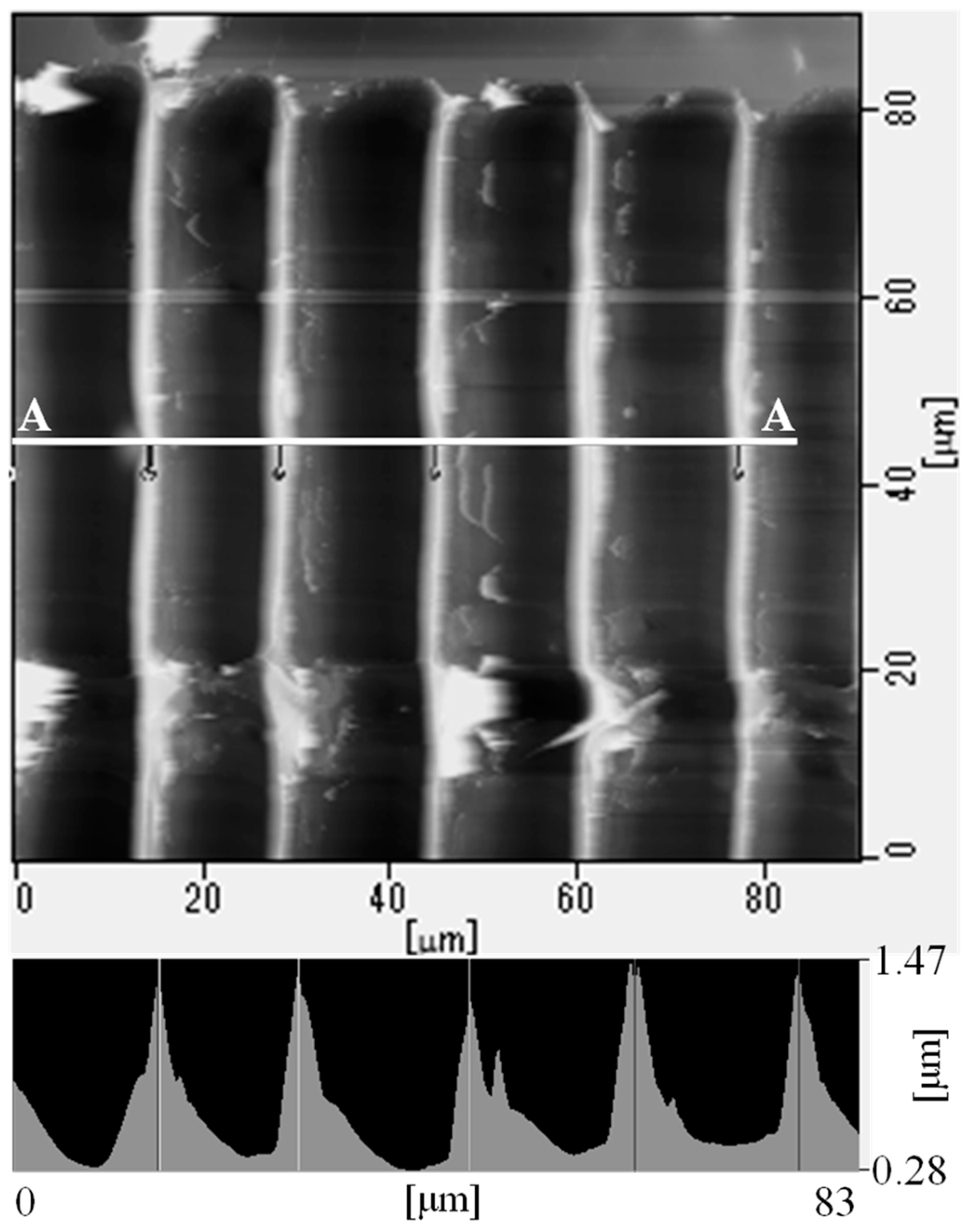
2.4. Observation of Surface Morphology and Measurement of the Formed Structure

We observed the surfaces of the PET and metal/PET films before and after SS processing using scanning electron microscopy (SEM) (S-4300, Hitachi High-Technologies, Minato-ku Tokyo, Japan) and scanning probe microscopy (SPM) (AFM 5400 L, Hitachi High-Technologies, Minato-ku Tokyo, Japan). In addition, when a fine periodic structure was present on the surface of the PET film and metal/PET films after SS processing, its period and depth were measured using SPM in the same way as in previous papers [1,7]. Hereafter, the period of the fine periodic structure formed by SS processing will be referred to as the structural period, and the depth of that structure will be referred to as the structural depth.

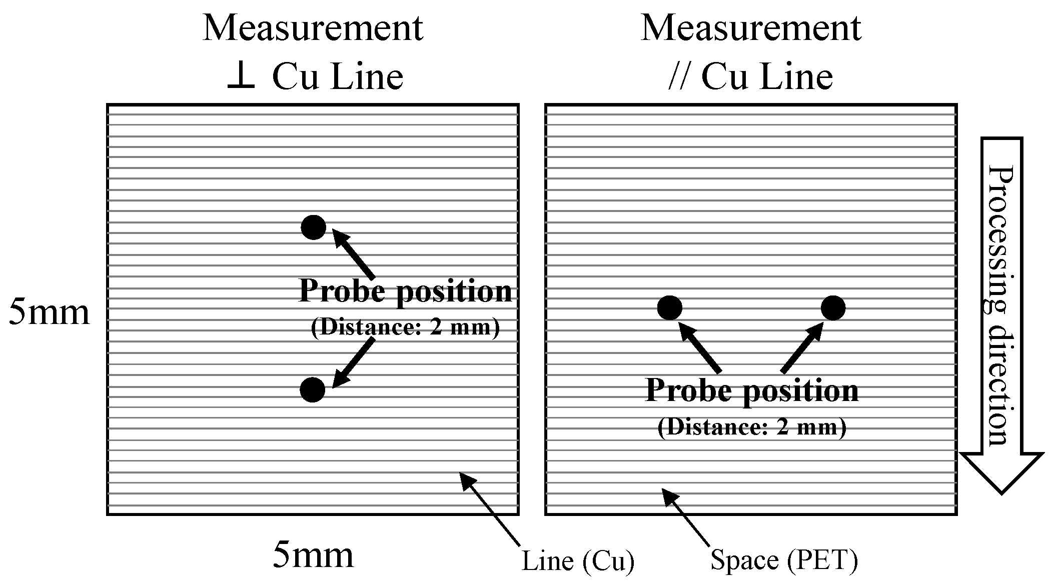
2.5. Measurement of Electrical Conductivity and Evaluation of its Anisotropy

The electrical conductivity and anisotropy of the surface of the SS-processed Cu/PET film were evaluated. Sheet resistance [Ω/sq.] needed to be measured using the four-probe method because resistance [Ω] is influenced by the distance between the probes. However, in this study, conductivity [S/m] was calculated from the resistance measurements for the reasons described below. For resistance measurements, we used a digital multimeter (CDM-16D, CUSTOM) and ten specimens (5 mm × 5 mm) cut from the SS-processed Cu/PET films (one specimen from each film). The probe interval was fixed at 2 mm (each probe located 1 mm from the center of film) (Figure 2). In order to evaluate the anisotropy, this measurement was performed in two directions: parallel and perpendicular to the Cu line.

3. Results and Discussion

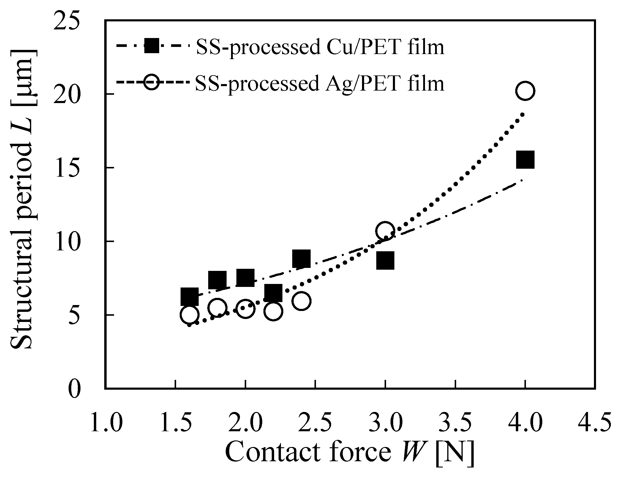
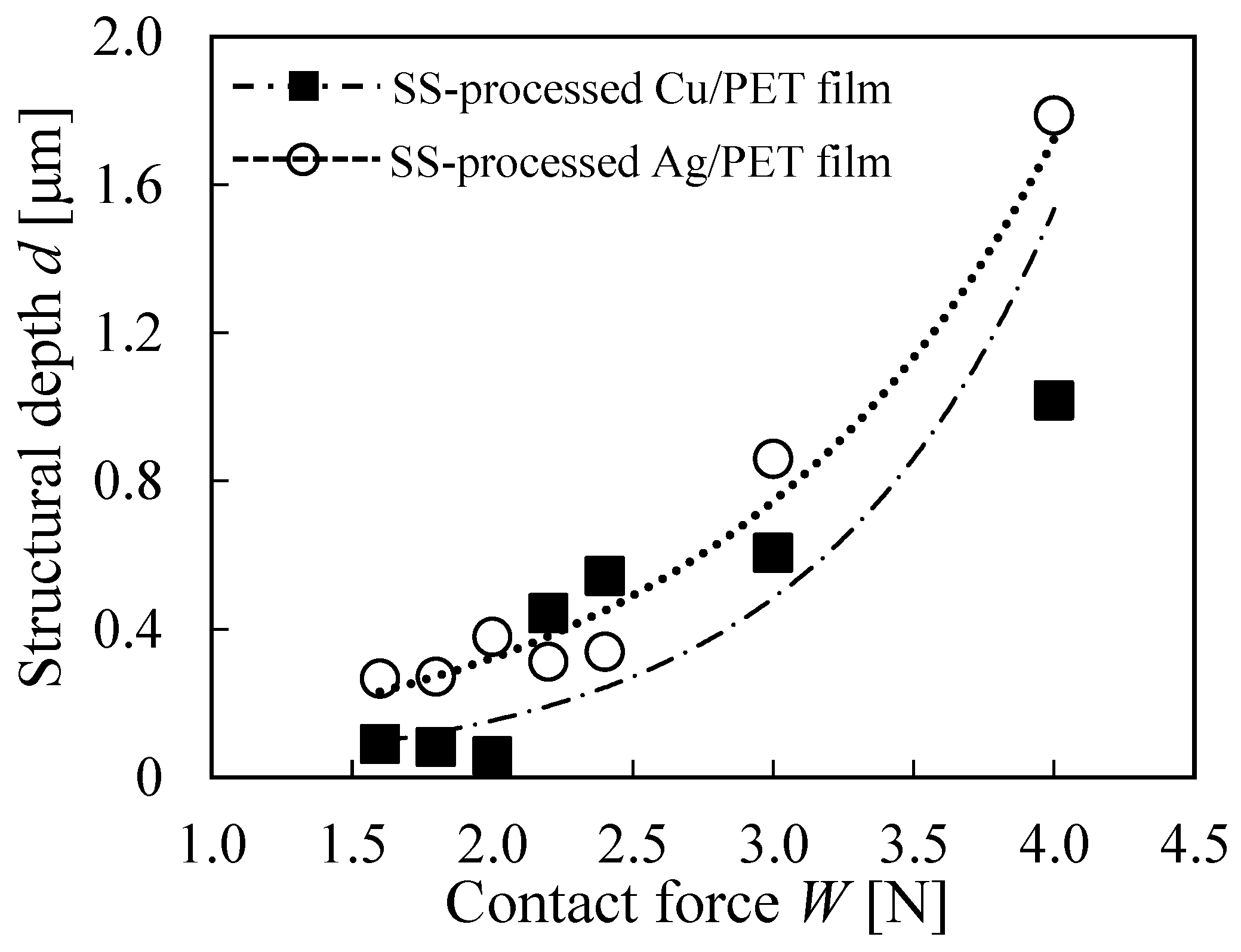
3.1. Relationship between the L/S-Like Pattern and Contact Force of SS Processing

Figure 3 and Figure 4 show the SPM images of the SS-processed PET Film and Cu/PET film, respectively. In both figures, the horizontal direction is the SS processing direction, the top images represent surface images, and the bottom images represent the cross-sectional profiles corresponding to the A–A section in the top figures. Stripes are observed in the vertical direction in the top images (height increases as contrast becomes brighter), and wavy periodic structures are observed in the horizontal direction in the bottom figures.
In principle, SS processing can be applied to any material as long as SS occurs. From Figure 3, it is clear that fine periodic structures can form using SS processing on PET. Moreover, the results in Figure 4 proved that SS processing can also be applied to metals. Thus, our study clarified that SS processing can be applied to not only polymers but metals as well. However, in the case of the SS-processed Cu/PET film, whether the metal layer was maintained on the surface of the PET could not be judged only from the SPM images and was further determined by measuring the electric resistance of the surface. Figure 5 shows the relationship between the contact force and structural period of the SS-processed PET and metal/PET films, while Figure 6 shows the relationship between the contact force and structural depth. The structural period shortened and structural depth shallowed as the contact force decreased for both the samples. This occurred because the penetrated depth of the processing blade became shallower as the contact force decreased [1].
A mathematical model of SS without abrasion (Equations (1) and (2) below) has already been proposed by Nakano et al. [2,3] and is based on a single-degree-of-freedom system with Coulomb friction:
λ = ( μ s μ k ) W V m k
f ss = 1 2 k m ( 1 π + λ tan 1 λ )
where W [N] is the normal load (contact force), V [m/s] is the driving speed, k [N/m] is the stiffness (spring constant), m [g] (= W/g, g [m/s2]) is the mass, μs is the static friction coefficient, μk is the kinetic friction coefficient, λ is a dimensionless parameter (known as the SS parameter), and fss [s−1] is the frequency. The wavelength of SS (moving distance of the contact point) Lss [m] can be expressed as follows:
L ss = V / f ss .
As mentioned above, Equations (1)–(3) are models of SS that do not account for the influence of abrasion [4,5,6]. Therefore, this model cannot quantitatively predict SS accompanying abrasion processes such as in SS processing. However, the model is useful for qualitatively predicting the relationship between processing conditions and the structural period. In fact, the wavelength of SS increases exponentially as the contact force increases in this model. This trend is in agreement with the tendency of SS processing (Figure 5). Thus, the L/S-like pattern can be adjusted by controlling the contact force.

3.2. Influence of Surface Material for SS Processing

When a blade is stabbed into a solid sample, its process shifts from pressing (elastic deformation) to indentation (plastic deformation) and further to cutting [9]. The tip shape of the razor used in this study was a macroscopically sharp triangle. However, the curvature radius of the tip of the razor was 2.91 μm; therefore, it can be regarded as a cylinder microscopically. Equation (4) expresses the maximum contact pressure pmax [Pa] obtained from the Hertzian theory [10] for the contact between a cylinder and a plane:
p max = F π R L cyl 1 ( 1 ν 1 2 ) / E 1 + ( 1 ν 2 2 ) / E 2
where F [N] is the pressing force (= W), Lcyl [m] is the width of a sample, R [m] is the curvature radius of the tip of the razor, ν1 is the Poisson’s ratio of the razor, ν2 is the Poisson’s ratio of the sample, E1 is the Young’s modulus of the razor, and E2 is the Young’s modulus of the sample. In the Hertzian theory, in the case of contact between a ball and a plane, the elastic displacement can be obtained from the pressing force. However, in the case of contact between a cylinder and a plane, the elastic displacement cannot be obtained from the pressing force, because its state is a plane strain state. On the other hand, the elastic displacement h [m] can be obtained geometrically as in Equation (5), although it is not synonymous with the elastic displacement of Hertzian theory.
h = R R 2 4 F R π L cyl ( 1 ν 1 2 E 1 + 1 ν 2 2 E 2 ) .
During SS processing, the sample is plastically deformed because the razor penetrates into the sample. Unfortunately, there is no theory that can predict an indentation (plastic deformation) process without empirical parameters. However, it is unlikely that a blade will easily penetrate a sample during an indentation process since it is hard to press a blade into a sample during a pressing process. Therefore, the relationship between the contact force and the penetrated depth was qualitatively examined using the above equation. From Equation (5), the elastic displacement deepens as the Young’s modulus of the surface material becomes lower. Generally, the Young’s modulus of Cu is bigger than that of Ag. Therefore, the structural depth of the SS-processed Cu/PET film was shallower than that of the SS-processed Ag/PET film (Figure 6).

3.3. Electrical Conductivity and its Anisotropy for the SS-Processed Cu/PET Film

Figure 7 shows a SEM image of the surface of the SS-processed Cu/PET film. Figure 8 presents a schematic of the ideal L/S-like pattern of the SS-processed Cu/PET film determined using the results from Figure 4 and Figure 7. As can be seen in Figure 7, the L/S-like pattern was broken in some places. This is due to the number of microscratches irregularly generated parallel to the processing direction due to the inherent defects at the tip of the processing blade (Figure 9).
The measured sheet resistance almost invariably incorporated the influence of microscratches when the four-probe test (distance between probes at both ends: 6 mm) was carried out during the preliminary experiments. Therefore, in this study, in order to eliminate the influence of microscratches as much as possible, the sheet resistance was calculated using the method described in the previous section.
Table 4 shows the conductivity of the SS-processed Cu/PET films and the presence or absence of anisotropic conductivity. Specimens #2, #3, and #9 have anisotropic conductivity: they conduct electricity in a direction parallel to the Cu line (perpendicular to the SS processing direction) and do not conduct electricity in a direction perpendicular to the Cu line (parallel to the SS processing direction). Thus, it was proved that the SS-processed Cu/PET film is an anisotropic conductive film. From Figure 4 and Figure 7 and Table 4, the surface metal layer is considered to be periodically scraped off as illustrated in Figure 8. However, the event probability of anisotropic conductivity of the film was remarkably low and the reproducibility was also poor. This was due to the influence of the inherent defects of the tip of the processing blade, as mentioned above.
Here, electrical conductivity values in the directions parallel and perpendicular to the Cu line were predicted by the rule of mixture. From Figure 7, when a comparatively narrow Cu line was chosen, both the width of the Cu line and the space (PET film) were approximately 4.4 μm. The electrical conductivities of the surface of the Cu/PET film and the PET film were 8.06 mS/m and 0 mS/m, respectively. Thus, the predicted values in the directions parallel and perpendicular to the Cu line are 4.03 mS/m (= 8.06 mS/m × 0.5) and 0 mS/m, respectively. In contrast, the averages of the electrical conductivities of specimens # 2, # 3, and # 9 were 0.28 mS/m and 0 mS/m in the directions parallel and perpendicular to the Cu line, respectively. This is because disconnection of the Cu line occurred in many places due to scratches caused by the inherent defects of the tip of the razor, as seen in Figure 7.
Preparing a defect-free blade is one solution for the problem of electrical conductivity, but the best solution to eliminate these inherent defects completely has not yet been found. However, given some of our successful experiments, this study clarified that SS processing has potential as a method for fabricating anisotropic conductive films with a simple L/S-like pattern. In addition, it is possible that the L/S-like pattern of the SS-processed Cu/PET film is in the submicron range, because the structural period of the SS-processed PET film was in the submicron range for some SS processing conditions [1]. Moreover, high-speed processing can be performed as long as SS occurs, and large-area processing can also be performed using wide blades.

4. Conclusions

In this study, we attempted to perform SS processing of a PET film with a surface metal layer. The findings of our study can be summarized as follows:
(1)
When the metal/PET film underwent SS processing, a fine periodic structure formed on the surface of the film because the metal layer was periodically scraped due to the occurrence of SS. Thus, an L/S-like pattern could be formed on the PET film using SS processing.
(2)
A fine periodic structure could be formed on both PET films and metal layers. Thus, it was proved that SS processing can be applied not only to polymers but also to metals.
(3)
The structural period shortened as the contact force decreased for both the SS-processed metal/PET film and the SS-processed PET film. Moreover, the structural depth, corresponding to the height of the metal line, became shallower in proportion to the structural period.
(4)
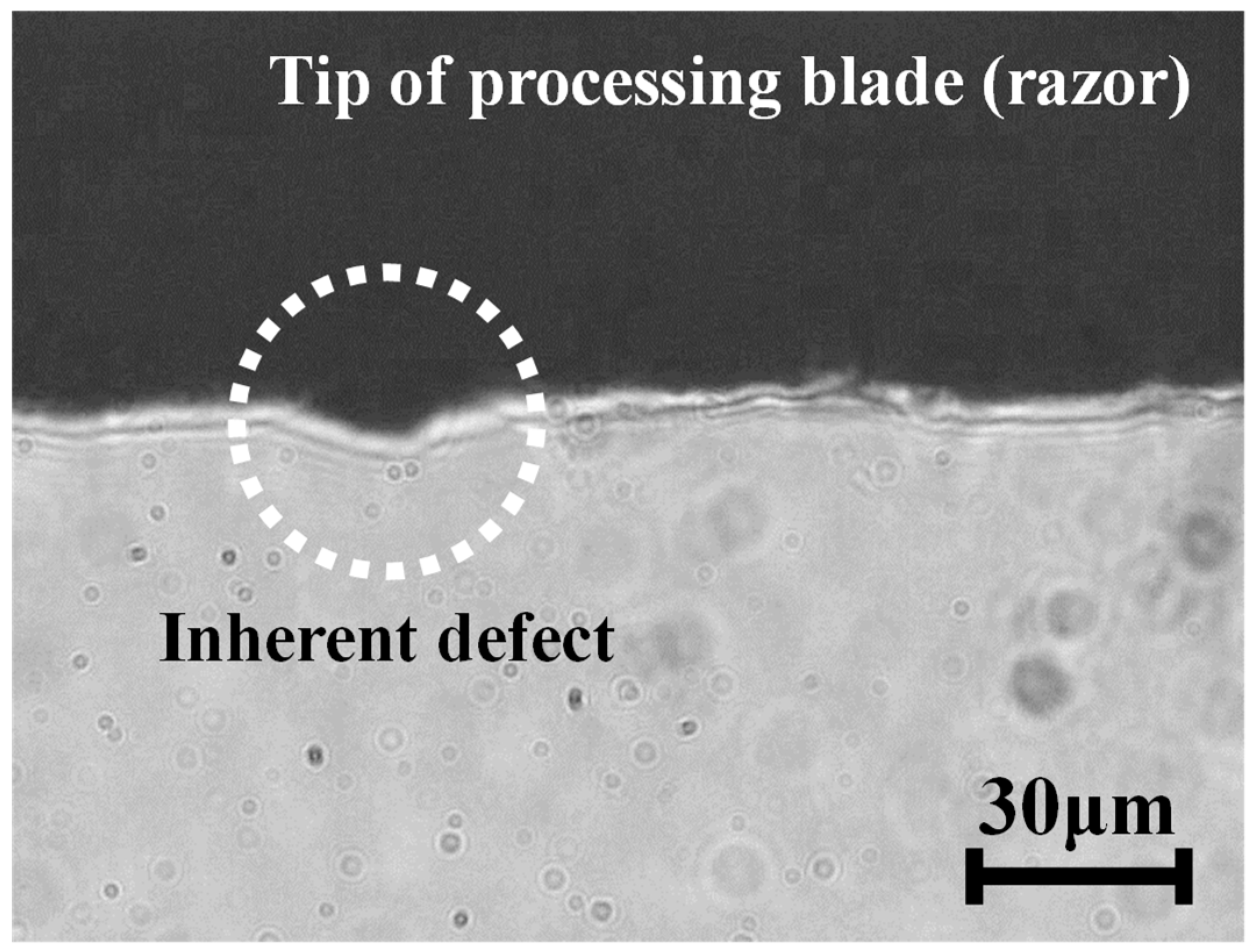
The SS-processed Cu/PET film has anisotropic conductivity: it conducts electricity in the direction parallel to the Cu line (perpendicular to the SS processing direction) but is non-conductive in the direction perpendicular to Cu line (parallel to the SS processing direction). However, the fabrication yield of an anisotropic conductive film is remarkably low at present due to inherent defects at the tip of the processing blade.
An anisotropic conductive film with L/S-like patterns was fabricated using SS processing, although there are still yield problems. An expansion of the application range of SS processing is expected in the future.

Author Contributions

Conceptualization, methodology, validation, formal analysis, resources, data curation, writing—original draft preparation, writing—review and editing, visualization, project administration and funding acquisition, K.N.; investigation, Y.K. and K.N.; supervision, K.Y and K.N.

Funding

This research was supported by JSPS KAKENHI Grant Number JP18K13669.

Acknowledgments

The authors are grateful to Futamura Chemical Co. for providing the PET film.

Conflicts of Interest

The authors declare no conflict of interest.

References

  1. Naito, K.; Tsutsumi, T.; Yamada, T.; Yashiro, K. Processing method utilizing stick-slip phenomenon for formingperiodic micro/nano-structure. J. Mat. Proc. Technol. 2016, 238, 267–273. [Google Scholar] [CrossRef]
  2. Nakano, K. Two dimensionless parameters controlling the occurrence of stick-slip motion in a 1-DOF system with Coulomb friction. Trib. Lett. 2006, 24, 91–98. [Google Scholar] [CrossRef]
  3. Nakano, K.; Maegawa, S. Occurrence limit of stick-slip: Dimensionless analysis for fundamental design of robust-stable systems. Lubr. Sci. 2010, 22, 1–18. [Google Scholar] [CrossRef]
  4. Schallamach, A. Friction and abrasion of rubber. Wear 1958, 1, 384–418. [Google Scholar] [CrossRef]
  5. Fukahori, Y.; Yamazaki, H. Mechanism of rubber abrasion. Part I: Abrasion pattern formation in natural rubber vulcanizate. Wear 1994, 171, 195–202. [Google Scholar] [CrossRef]
  6. Wang, J.; Chen, B.; Yan, F.; Xue, Q.; Zhao, F. Pattern abrasion of ultra-high molecular weight polyrthylene: Microstructure reconstruction of worn surface. Wear 2011, 272, 176–183. [Google Scholar] [CrossRef]
  7. Naito, K.; Yamada, T.; Tsutsumi, T.; Yashiro, K. Wettability of a microgrid-structured polymer film with microfabrication utilizing the stick–slip phenomenon. J. Appl. Polym. Sci. 2017, 134, 45140. [Google Scholar] [CrossRef]
  8. Naito, K.; Nimura, K.; Yashiro, K. Influence of frictional vibration on wear when razor rubs polypropylene single fiber. J. Fiber Sci. Technol. 2018, 74, 47–52. [Google Scholar] [CrossRef]
  9. McCarthy, C.T.; Hussey, M.; Gilchrist, M.D. On the sharpness of straight edge blades in cutting soft solids: Part I–indentation experiments. Eng. Fract. Mech. 2007, 74, 2205–2224. [Google Scholar] [CrossRef]
  10. Timoshenko, S.P.; Goodier, J.N. Theory of Elasticity, 3rd ed.; McGraw-Hill: New York, NY, USA, 1970. [Google Scholar]
Figure 1. Schematic of the stick-slip processing device.
Jmmp 03 00060 g001
Figure 2. Measurement of electrical resistance and evaluation of anisotropic electrical conduction for SS-processed Cu/PET films.
Jmmp 03 00060 g002
Figure 3. Scanning probe microscopy (SPM) images of the SS-processed PET film at W = 2.54 N (T = 4.90 N, θ = 150.0°): surface image (top) and cross-sectional profile at the A–A section in the surface image (bottom). Processing conditions: V = 10.0 mm/min and L = 1.0 mm.
Jmmp 03 00060 g003
Figure 4. SPM images of the SS-processed Cu/PET film at W = 4.00 N (T = 7.73 N, θ = 150.0°): surface image (top) and cross-sectional profile at the A–A section in the surface image (bottom). Processing conditions: V = 10.0 mm/min and L = 1.0 mm.
Jmmp 03 00060 g004
Figure 5. Contact force dependence of the structural period for the SS-processed metal/PET films. Processing conditions: T = 3.09–7.73 N, θ = 150.0°, V = 10.0 mm/min, and L = 1.0 mm.
Jmmp 03 00060 g005
Figure 6. Contact force dependence of structural depth for the SS-processed metal/PET films. Processing conditions: T = 3.09–7.73 N, θ = 150.0°, V = 10.0 mm/min, and L = 1.0 mm.
Jmmp 03 00060 g006
Figure 7. SEM image of the SS-processed Cu/PET film at a W = 3.0 N contact force. Processing conditions: T = 5.80 N, θ = 150.0°, V = 10.0 mm/min, and L = 1.0 mm.
Jmmp 03 00060 g007
Figure 8. Schematic of the ideal line and space (L/S)-like pattern of the SS-processed Cu/PET film.
Jmmp 03 00060 g008
Figure 9. Inherent defect at the tip of the processing blade.
Jmmp 03 00060 g009
Table 1. Mechanical properties of materials.
ItemPET Film (FE2000)TE-2 Sheet
Young’s modulus E [GPa]4202
Tensile strength σ [MPa]172325
Table 2. Friction coefficients between materials.
ItemPET Film
TE-2 Sheet
Cu/PET Film
TE-2 Sheet
Ag/PET Film
TE-2 Sheet
Static friction coefficient μs0.2160.1800.166
Kinetic friction coefficient μk0.1580.1610.152
Table 3. Stick-slip (SS) processing conditions.
Processing LoadProcessing SpeedProcessing AngleFree-Edge Length of Blade
T [N]V [mm/min]θ [°]L [mm]
3.09–7.7310.0150.01.0
Table 4. Evaluation of anisotropic conductivity for SS-processed Cu/PET films.
Specimen Number12345678910
Electrical conductivity [mS/m]
⊥ Cu line
0.000.000.000.000.740.710.000.000.012.00
Electrical conductivity [mS/m]
// Cu line
0.000.120.590.001.300.830.000.000.122.90
Anisotropic conductive-------
The surface electrical conductivity values of PET and Cu/PET were 0 and 8.06 mS/m, respectively. Processing conditions: W = 3.0 N (T = 5.80 N, θ = 150.0°), V = 10.0 mm/min, and L = 1.0 mm.

