1. Introduction
The superlattice (SL) based on III-V materials has recently shown significant development in infrared (IR) detector technology. Fundamental properties of SLs provide several advantages in comparison to the HgCdTe alloy:
large splitting between heavy-hole and light-hole valence sub-bands due to strain in SLs contributes to the suppression of Auger generation-recombination (GR) mechanisms;
not directly bandgap energy dependent effective masses leading to reduction of tunneling currents in SL detectors
less ionic chemical bonding of III-V semiconductors leading to better stability.
InAs/GaSb SLs have a type II misaligned band offsets between InAs and GaSb. The conduction band (CB) level of InAs is lower than the valance band (VB) of GaSb, what creates a spatial separation of electrons and holes in the InAs/GaSb heterostructure. The bandgap is determined by the energy difference between the electron miniband C1 and the first heavy hole state HH1 at the Brillouin zone center. However, GaSb layer in InAs/GaSb SLs impose the carrier lifetime limitations [
1,
2]. For materials with the same cut-off wavelength, a significant longer minority carrier lifetime has been obtained in the InAs/InAsSb SL system (Ga-free SLs) in comparison to the InAs/GaSb SLs.
InAs/InAsSb SLs are in the early stage of development and are less studied than InAs/GaSb counterparts. Due to only two common elements (In and As) in SL layers and a relatively simple interface structure with Sb-changing element, the InAs/InAsSb SL growth is characterized by a better controllability and a simpler manufacturability.
The sophisticated physics associated with type-II superlattices (T2SLs) gave a new impact on detector design by introducing a class of IR detectors named barrier detectors [
3,
4,
5,
6]. The most popular is the nBn structure, where the n-type semiconductor on one side of barrier is a contact layer for device biasing, while the n-type semiconductor on the other side is absorber with a thickness comparable to the absorption length. This structure is a hybrid between a photoconductor and a photodiode. An unipolar barrier blocks one carrier type (electrons) but allow the unimpeded flow of the other (holes). The introduction of the wide bandgap barrier instead of depletion layer causes the suppression of Shockley-Reed-Hall (SRH) thermal GR contribution to dark current. This generates lower dark current and creates condition for higher detector operating temperature.
2. Experimental Results
Detector’s epitaxial structure was grown on GaAs (001) substrate by a solid source RIBER COMPACT 21 DZ molecular beam epitaxy (MBE) system, equipped with standard effusion cells for gallium (Ga) and indium (In), and with valve cracked cells for arsenic (As) and antimony (Sb) [
7]. As
4 and Sb
2 have been used. In situ RHEED (Reflection High Energy-Electron Diffraction) was used to monitor the growth process. The crystallographic properties of the samples, as well as Sb mole fractions were determined using a high-resolution X-ray diffractometer of PANalytical X’Pert.
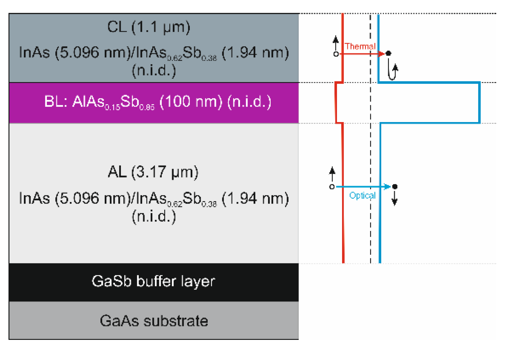
In order to achieve low dark currents, the nBn device architecture was used. The barrier layer (BL) material was a bulk AlAs
0.15Sb
0.85 while InAs/InAsSb SL was used for the absorber layer (AL) and contact layer (CL). The whole structure was non-intentionally doped (n.i.d.) what provides n-type conductivity. Details of the nBn detector structure are given in
Figure 1.
To determine the position of the CB and VB and ensure a correct band alignment between the BL and AL, we have used a k·p model which can also predict the absorption spectrum and the cut-off wavelength of the AL, from a knowledge of the thicknesses of the InAs and InAsSb in each superlattice period.
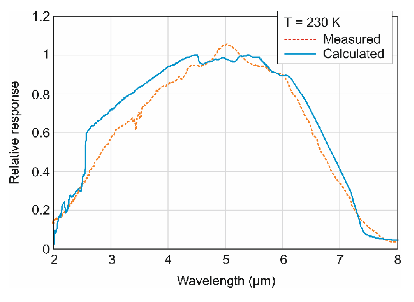
Figure 2 compares the spectral response of the nBn T2SL detector measured at 230 K with the simulated spectrum based on the k·p calculations with a commercial APSYS software. It can be seen that a good agreement was obtained by the simulation, for the T2SL with the thicknesses of the InAs layer of a 5.096 nm and InAs
0.62Sb
0.38 layer of a 1.94 nm in each superlattice period. The obtained 50% cut-off wavelength is of about 6.7 µm at 230 K.
Figure 3 displays the calculated band diagram of the chosen InAs (5.096 nm)/InAs
0.62Sb
0.38 (1.94 nm) T2SL structure at 230 K. The figure also shows the probability distribution functions for electrons and heavy holes. Electrons are confined in the InAs layer, whereas holes are confined to the InAsSb layer, therefore the transition occurs only where the probability distribution functions overlap.
For heterostructure devices, the consideration of the CB and VB alignments that result when the materials are joined is necessary. Especially in the nBn design, the valence band offset (VBO) and the conduction band offset (CBO) are important parameters which governs carrier blocking and transport throughout the heterostructure. The CB and VB position as a bulk parameter for binary compounds (InAs, InSb, AlAs and AlSb) can be subtracted to determine the relative band alignment between each materials. To derive bands position for an AlAsSb ternary alloy, linear interpolation between the pure corresponding materials can be used. The position of the VB edge for the AlAs
1-xSb
x ternary material can be calculated from the dependence:
where
CVB is the VB bowing parameter often given in the literature. Ref. [
8] provides the value of the
CVB of −1.71 eV for AlAsSb alloys lattice matched to GaSb. It is difficult to determine which bowing is in the case of thin layer sandwiched between two SLs, thus in our calculations, the VB bowing for AlAsSb was a matching parameter. As the results show, it strongly influences the bands alignment, and hence transport of carriers.
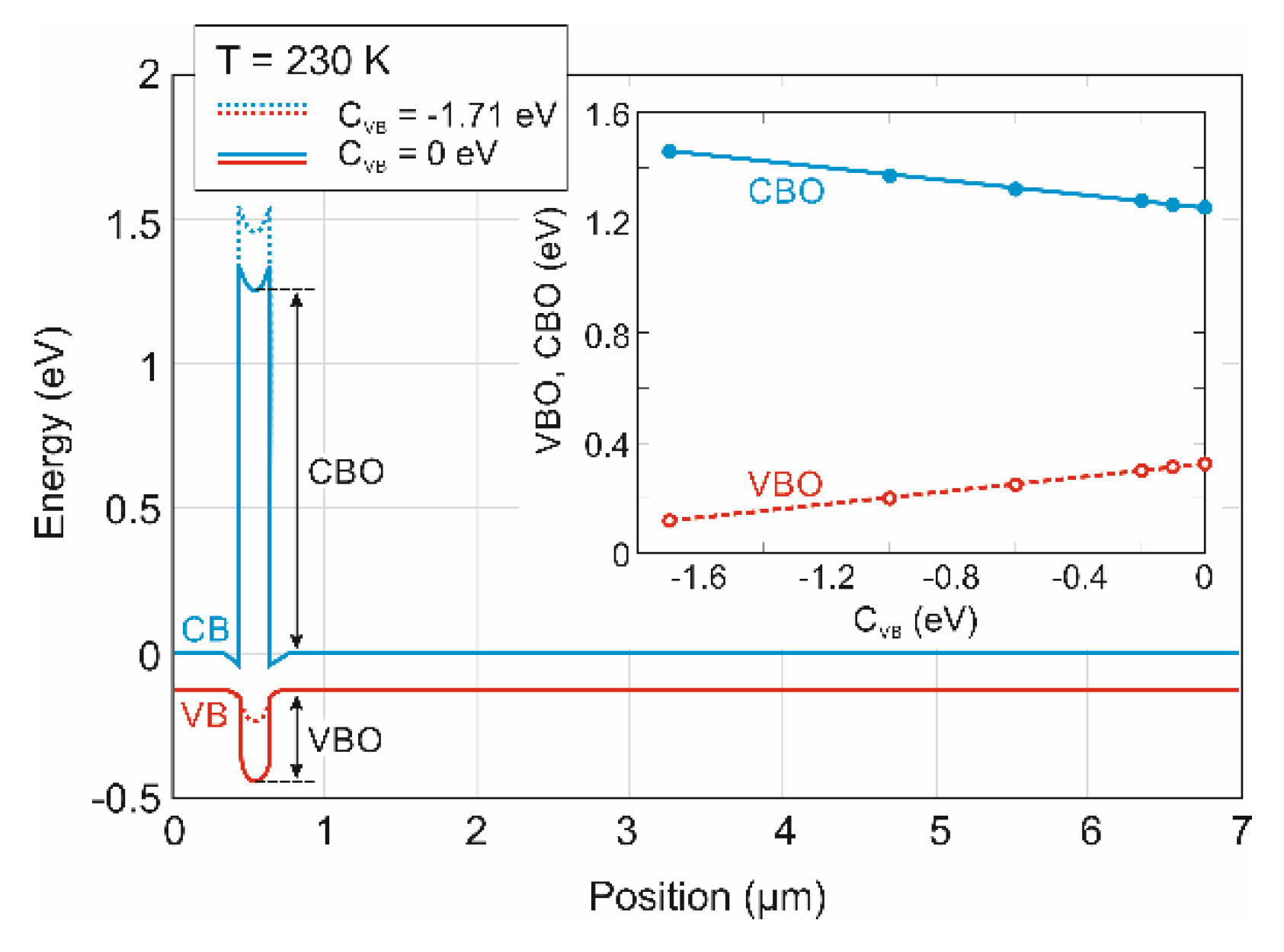
Figure 4 shows calculated band diagram for unbiased nBn T2SL detector operated at 230 K. The CB and VB alignments have been calculated for different values of the VB bowing for AlAsSb. The VBO and CBO as a function of the VB bowing parameter for AlAsSb is presented inset
Figure 5. In any case, the height of the barrier in the CB is large enough to block the flow of electrons. The height of the barrier in the VB determines the value of dark currents.
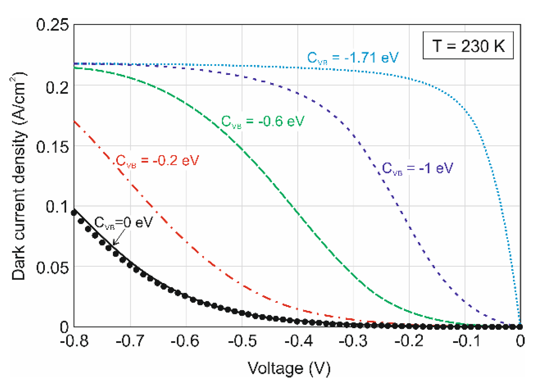
Figure 5 shows the measured current-voltage characteristic for the nBn T2SL detector operated at 230 K and calculated plots for different values of the VB bowing for AlAsSb. Very good fit of the calculated plot to the experimental data was obtained for a zero VB bowing parameter for AlAsSb layer. Sufficiently high barrier in the VB, of 318 meV, blocks both the flow of electrons and holes, hence extremely low dark current densities are observed. The lack of the current responsivity is also the consequence of large VBO. Nearly zero VBO can be obtained assuming
CVB = −1.71 eV. The barrier of 113 meV in the VB allows for the flow of holes after biasing the detector with relatively low voltage. This causes an increase of current responsivity, but also an increase dark currents due to the current of minority carriers. Nevertheless, in our case it is not possible to obtain a correct band alignment between the AlAs
0.15Sb
0.85 BL and the InAs (5.096 nm)/InAs
0.62Sb
0.38 (1.94 nm) T2SL AL. Thus in further works we examine an AlInSb ternary alloy for the BL, as a material potentially better aligned to the AL.
