Proceeding Paper

Miniaturized Plasma Actuator Flow Measurements by MEMS-Based Thermal Conductivity Sensors †

by
Dominik Berndt
1,*,
Matthias Lindner
1,
Karl Tschurtschenthaler
2,
Christoph Langer
1 and
Rupert Schreiner
1
1
Faculty of General Sciences and Microsystems Technology, OTH Regensburg, 93047 Regensburg, Germany
2
Faculty of Mechanical Engineering, OTH Regensburg, 93047 Regensburg, Germany
*
Author to whom correspondence should be addressed.
Presented at the Eurosensors 2018 Conference, Graz, Austria, 9–12 September 2018.
Proceedings 2018, 2(13), 939; https://doi.org/10.3390/proceedings2130939
Published: 19 December 2018
(This article belongs to the Proceedings of EUROSENSORS 2018)

Abstract

:
The gasflow created by a minaturized dielectric barrier discharge (DBD) plasma actuator is measured by a MEMS-based thermal conductivity gas sensor giving an indication of flow velocity and flow direction. The possiblity of several sensors in a small area gives a far better accuracy of local flow phenomena compared to conventional sensors. This is important for a better understanding of plasma- induced flow characteristics.

1. Introduction

Micro-plasma discharges arranged in the geometric shape of a miniaturized DBD actuator cause ionic wind behind the exposed electrode resulting in a gas flow due to conservation of momentum [1]. Established measuring methods have the disadvantage that the flow generated by a miniaturized plasma actuator is strongly influenced by the sensor itself, like it is the case with Pitot-tubes [2], whereas techniques like particle imaging velocimetry (PIV) require a more complex setup and signal processing [3]. We present a new measurement method for micro DBD-plasma actuator flow using thermal conductivity MEMS-based surface hotfilms that provide a faster operating time, high frequency response and a less disturbing setup [4]. The measurement of the plasma-induced airflow could then be used to control and compensate the generation of instabilities leading to turbulent flow.

2. Material and Methods

2.1. Sensor Chip

A (100)-oriented silicon wafer serves as substrate material of the sensor. Front- and backside are covered with a layer of silicon nitride (SiN). Due to its low thermal conductivity it is suitable for building the sustaining filament structure. The pattern of the filament is defined by optical lithography and metallized with chromium and nickel; gold is used for the bondpads. The removal of the residual resist is done by a lift-off process in acetone. A further SiN layer is afterwards deposited on top of the metal film and creates an embedding of those structures. Subsequently the nitride layer is removed by reactive ion etching (RIE) at the places around the filament where an etching attack to the underlying silicon has to be provided and additionally above the gold bondpads for electrical contacting. Two sensor designs have been focused yet which can be seen in Figure 1.

2.2. Miniaturized Plasma Actuator

The miniaturized plasma actuator (PA) is realized on borofloat glass substrate with a thickness of 500 μm. Thereby front- and back-side are consecutively patterned by optical lithography and metallized with gold for cascaded HV-electrodes with sawtooth tips and chrome/copper for ground electrodes respectively. The lift- off process is done in acetone. The singularized sensor chips are glued onto the PA-wafer with a distance of a few mm regarding to the ground electrode which can be seen in Figure 2.

2.3. Measurement Setup

A constant current is applied to each of the two sensors on a chip by a HP semiconductor parameter analyzer acting as a DC source. The voltage experienced at the heated filament can be measured by a Keithley DMM. For plasma generation a function generator with a frequency of 1 kHz is used. A high voltage amplifier produces voltages up to 10 kV. The consumed power of the plasma actuator can be calculated from a measurement of the induced current of a Rogowski coil. All measurements are performed in constant current mode by measuring the voltage experienced on the sensor.

3. Results

The first measurement is performed with a chip of the design C1. The chip consists of two sensors, where one filament is freely suspended over a completely etched trench whereas the other is not under-etched and therefore has high thermal losses into the silicon substrate. A constant current is applied to the sensor filament. The electrical resistance and therefore the voltage of the metal film decreases during DBD-induced gas flow. Figure 3 shows the behavior of both sensors. The filament located on the freely suspended membrane shows a much lower rise time in contrast to the filament that is directly coupled to the substrate. The fall time of the freely suspended filament moreover is smaller than the substrate-coupled filament. To get a better understanding of the behavior of the sensors in dependence of the plasma voltage and distance to the PA, a sensor of the design D3 was exposed to different high voltages from 1.65 kV to 6.6 kV.
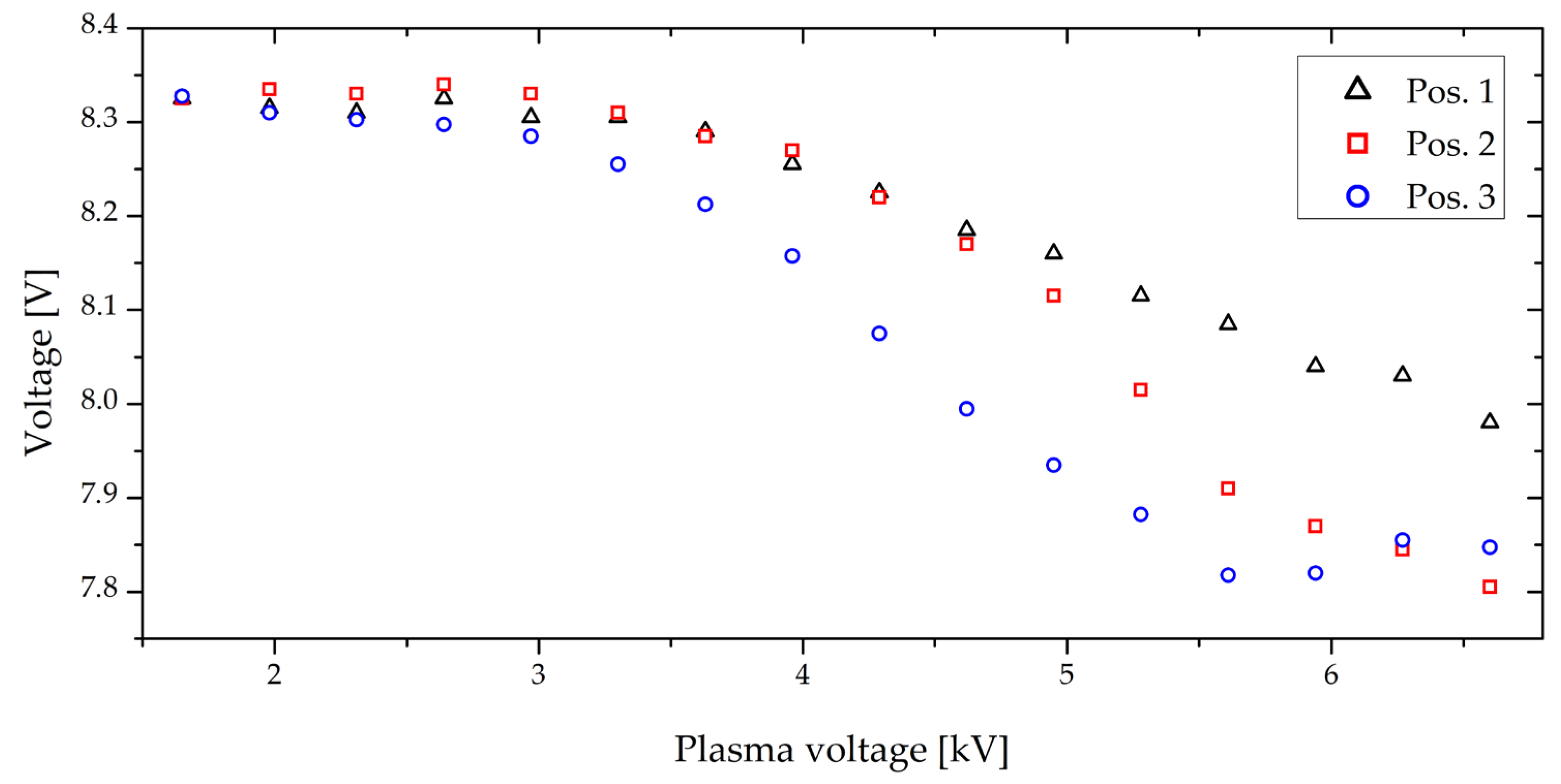
Figure 4 shows the plot of the sensor voltage over the plasma voltage for three different positions Pos. 1 (25 mm), Pos. 2 (15 mm) and Pos. 3 (5 mm) respectively to the ground electrode. The closer to the PA the heavier is the cooling due to the plasma induced airflow. Placed directly next to the PA at Pos. 3, the sensor voltage seems to be saturated at high plasma voltages.
Figure 5 shows a plot of the sensor voltage over the time with two different high voltages. The voltage drops during the plasma operation and the fluctuations are due to the high superimposed electrical field generated by the plasma source. A FFT was done for the area of 5.9 kV operation voltage by Origin showing a frequency of 1 kHz which matches the driving frequency of the plasma source. To get the frequency contribution of the airflow itself the sensor was shielded by a glass slide and two measurements with and without shielding were performed. The distance of the sensors remained the same between the two measurements, so it can be assumed that the electrical field has not changed. The subtraction of the signals therefore results in the flow component induced by the DBD plasma actuator and the electrical field can be eliminated.
The voltages of the shielded and unshielded setups are plotted in Figure 6. The difference in amplitude between both setups is about 350 mV and arises from the DBD induced airflow that cools the sensor that is not shielded by a glass slide. The subtraction of the phase-matched voltages gives the signal of the airflow, when the electrical field is eliminated.

4. Discussion and Outlook

We have shown that the voltage drop of the heated filament during plasma operation is due to the plasma- induced airflow, shielding of the sensor results in no voltage drop. Increasing the PA voltage results in a stronger flow, increasing the distance of the sensor to the PA makes the flow weaker. Attempts to eliminate the parasitic frequency created by the electric field of the plasma source demonstrate that there is a non-zero contribution of the airflow itself what is important for subsequent applications of the plasma actuator as an active flow control device. The sensor could then be used to figure out frequencies of the airflow instabilities. With this information the DBD plasma actuator could be driven in an intelligent control circuit for in-situ damping of e.g., Tollmien-Schlichting waves. Next steps are the realization of sensor and plasma actuator on one single substrate and the calibration of the combination in laminar flow.

Author Contributions

D.B., C.L. and R.S. conceived and designed the experiments; D.B. and M.L. performed the experiments; D.B. and K.T. analyzed the data; C.L. fabricated the samples; D.B. and R.S. wrote the paper.

Acknowledgments

We gratefully acknowledge the Bayerisches Wissenschaftsforum BayWISS especially the Verbundkolleg Ressourceneffizienz & Werkstoffe.

Conflicts of Interest

The authors declare no conflict of interest. The founding sponsors had no role in the design of the study; in the collection, analyses, or interpretation of data; in the writing of the manuscript, and in the decision to publish the results.

References

  1. Maden, I.; Maduta, R. Experimental and computational study of the flow induced by a plasma actuator. Int. J. Heat Fluid Flow 2013, 41, 80–89. [Google Scholar] [CrossRef]
  2. Wang, L.; Wong, C.W.; Lu, Z.; Wu, Z.; Zhou, Y. Novel Sawtooth Dielectric Barrier Discharge Plasma Actuator for Flow Separation Control. AIAA J. 2017, 554, 1405–1416. [Google Scholar] [CrossRef]
  3. Simon, B.; Markus, D.; Tropea, C. Cancellation of Tollmien-Schlichting Waves in Direct Vicinity of a Plasma Actuator. AIAA J. 2018, 1–10. [Google Scholar] [CrossRef]
  4. Dams, F.; Schreiner, R. Influencing factor of the sensitivity of MEMS-based thermal conductivity vacuum gauges. J. Vac. Sci. Technol. A 2014, 32, 031603. [Google Scholar] [CrossRef]
Figure 1. Sideview of design D3 (left) and C1 (right) The etching trench of design D3 has a depth of ~150 μm, whereas at design C1 the silicon underneath the filament is completely removed by etching from the backside.
Proceedings 02 00939 g001
Figure 2. (a) Measurement setup for the sensor chip and the plasma actuator HV source. (b) General scheme of the combined device: The hotfilm sensor chip is glued onto the wafer in streamwise direction of the cascaded plasma actuators and bonded to copper leads where the electrical contacting is performed.
Proceedings 02 00939 g002
Figure 3. (a) Comparison of the rise times between a freely suspended filament and one coupled to the silicon. The sensitivity of the filament which is under-etched is much better than the one without under-etching (b).
Proceedings 02 00939 g003
Figure 4. Voltage of the sensor as a function of the PA voltage for different positions of the sensor.
Proceedings 02 00939 g004
Figure 5. (a) Intervals of plasma operation at different high voltages (b) Focus on the plasma source generated fluctuations during operation at 5.9 kV.
Proceedings 02 00939 g005
Figure 6. (a) Voltage over time plot of the shielded and unshielded sensor. The amplitudes are about 50 mV (b) The subtraction of shielded and unshielded sensor voltages shows, that the amplitude has reduced below 5 mV.
Proceedings 02 00939 g006
Publisher’s Note: MDPI stays neutral with regard to jurisdictional claims in published maps and institutional affiliations.