Optimization of Si-Based Waveguides for Evanescent-Field Sensors †
by
 ,
,
Andreas Tortschanoff
1,* ,
,
Christian Ranacher
1,
Cristina Consani
1,
Thomas Grille
2 and
Mohssen Moridi
1 1
Carinthian Tech Research AG, 9524 Villach, Austria
2
Infineon Technologies Austria AG, 9500 Villach, Austria
*
Author to whom correspondence should be addressed.
†
Presented at the Eurosensors 2018 Conference, Graz, Austria, 9–12 September 2018.
Proceedings 2018, 2(13), 739; https://doi.org/10.3390/proceedings2130739
Published: 30 November 2018
(This article belongs to the Proceedings of EUROSENSORS 2018)
Abstract
:We present a detailed study of Si-based optical waveguides, which can be used as evanescent field sensors for the quantitative analysis of various gases and liquids. Direct quantitative comparison of simulation with experimental results of directional coupling structures allows fine-tuning the material parameters and provides important input for future sensor design.
1. Introduction
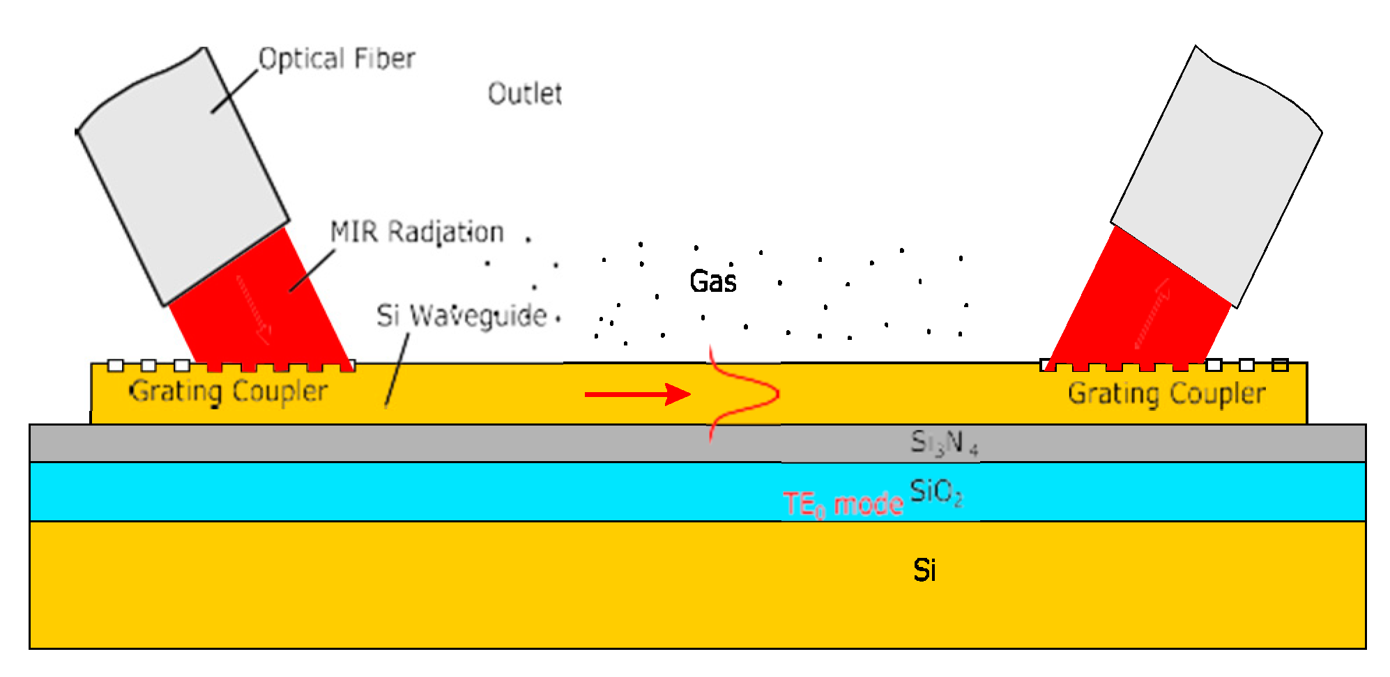
Interest for integrated gas sensors which could be used in mobile devices has grown over the last years and provides the motivation for investigating Si-based photonics in the mid-infrared spectral range [1]. One approach uses waveguide structures and evanescent field infrared absorption as the sensor principle. The radiation is guided in a suitable waveguide but part of the field extends into the cladding, and can interact with the analyte as shown in Figure 1.
2. Experimental
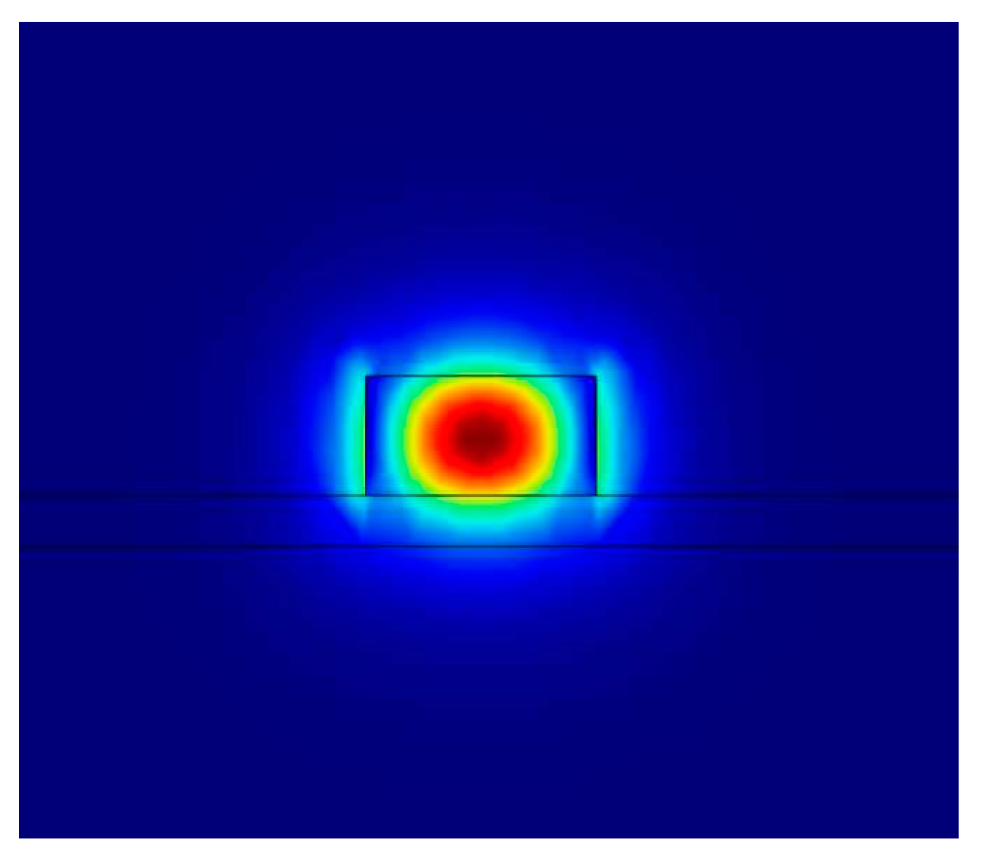
Simulations for designing the dimensions of the waveguide and the grating coupler where carried out using COMSOL-Multiphysics. The dimensions of the waveguide were designed for single-mode wave propagation and a typical calculated mode profile for a strip waveguide on a silicon nitride membrane is shown in Figure 2. Different thicknesses of the silicon nitride membrane were tested.
However, there are quite some uncertainties, connected to the optical parameters. The optical properties of the thin layer of poly-Si also depends on details of the deposition method, and can deviate a lot from literature values, found for crystalline silicon. The same is true for Si3N4 whose properties also depend on the details of the deposition method. In order to characterize our waveguides in detail, we designed directional couplers, the properties of which are very sensitive to the exact shape of the mode. A direct comparison between experiments and simulation thus allows fine-tuning the optical parameters for the simulation. A basic scheme of the layout is shown in Figure 3. The waveguides have a width and height of 1.4 µm and 660 nm, respectively. Light was coupled in and out via grating couplers and taper structures. For the structures measured in this paper, the gap between the waveguides was 400 nm. Measurements were performed at 4.26 µm, which is close to the absorption band of CO2, since CO2 sensing could be a possible application for these waveguides. In the experiments light from a quantum cascade laser is coupled in at port 1 via optical fibers and detectors are placed at port 2 (“through-port”) and 3 (“drop-port”).
3. Results
Measurements on structures with different interaction lengths allow quantitative comparison of the experimental results with the simulation. Simulations for different waveguide-geometries were performed with varying gap sizes and interaction lengths. Optical parameters of the materials were taken from literature [4]. (Specifically, the values used for the refractive indices of silicon and silicon nitride were nSi = 3.42, nSi3N4 =1.89, respectively.)
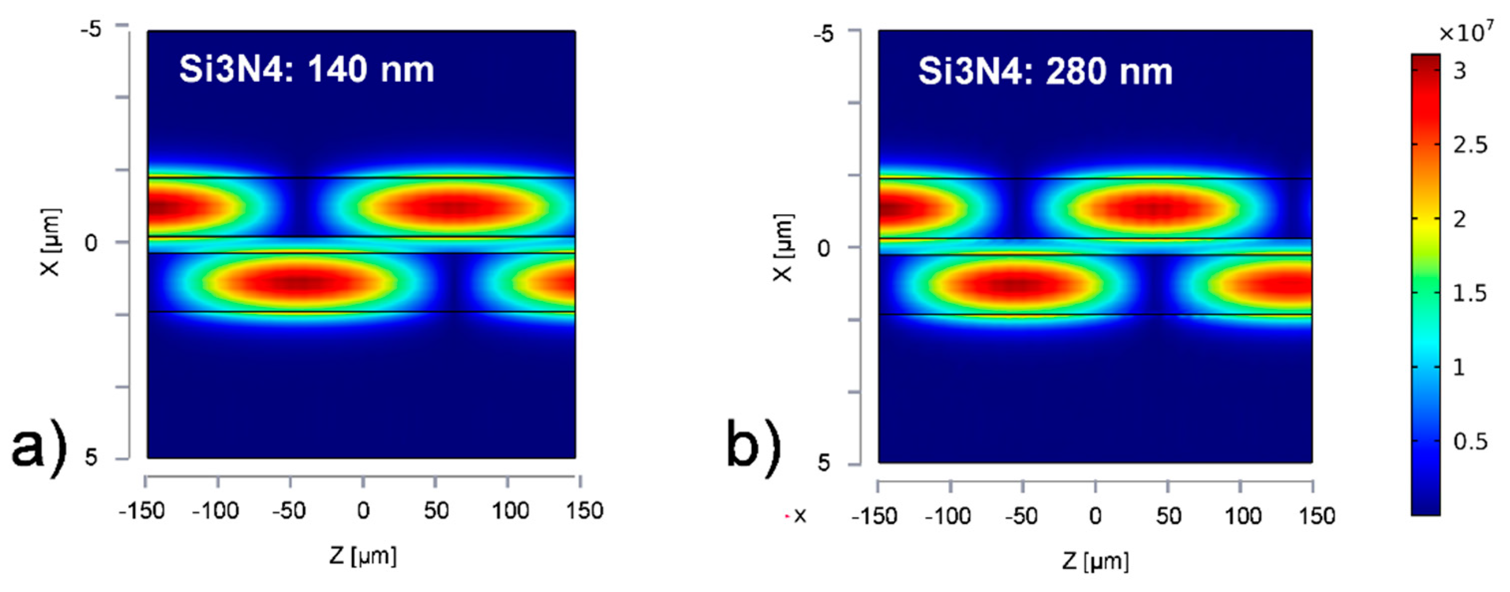
Figure 4 shows simulation results for two different thicknesses of the Si3N4 layer. From these simulations we estimated the coupling length for maximal energy transfer between the waveguides to be 110 µm and 95 µm for thicknesses of the Si3N4-layer of 140 nm and 280 nm, respectively.
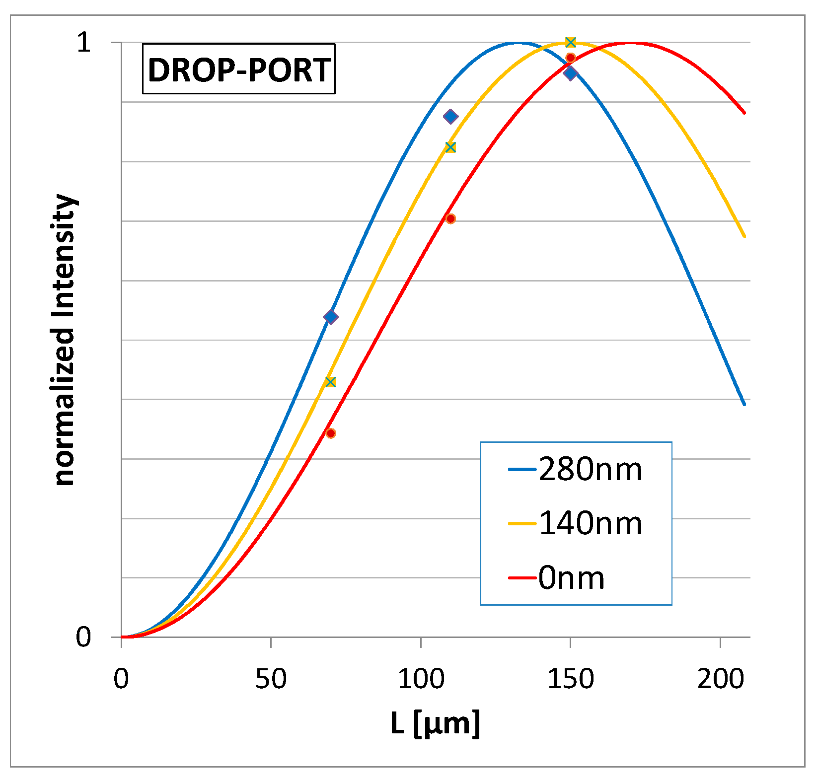
Based on the simulations, test-structures with interaction lengths of 70, 110, and 150 µm were designed and fabricated. Wafers with three different thicknesses of the silicon nitride layer were fabricated. In the experiments we measured the light coupled to the other waveguide by putting a detector at the drop-port. The results are plotted in Figure 5. We found a mismatch of about 20% with regard to the initial estimates of the coupling lengths. However, fine-tuning of the optical parameters nSi and nSi3N4 by some percent provides excellent overlap between experiment and simulation as can be seen in Figure 5. Among others, our results indicate, that the index of refraction of the deposited poly-silicon is about 3% higher in our structures, compared to literature values of bulk silicon.
4. Conclusions
We presented the design and a detailed characterization of silicon strip waveguides. Among others, our results indicate, that the index of refraction of the deposited poly-silicon is about 3% higher in our structures, compared to literature values of bulk silicon. Based on these results, we will proceed in designing and optimizing the next generation of waveguide structures for evanescent field sensing.
Acknowledgments
This work was performed within the Competence Centre ’ASSIC Austrian Smart Systems Integration Research Center’ and ’LCM Linz Centre of Mechatronics’, co-funded by the Federal Ministries of Transport, Innovation and Technology (BMVIT) and Digital and Economic Affairs (BMDW) and the Federal Provinces of Carinthia, Styria and Upper Austria within the COMET — Competence Centers for Excellent Technologies Programme.
Conflicts of Interest
The authors declare no conflict of interest. The founding sponsors had no role in the design of the study; in the collection, analyses, or interpretation of data; in the writing of the manuscript, and in the decision to publish the results.
References
- Lavchiev, V.; Jakoby, B. Photonics in the Mid-Infrared: Challenges in Single-Chip Integration and Absorption Sensing. IEEE J. Sel. Top. Quantum Electron. 2017, 23, 452–463. [Google Scholar] [CrossRef]
- Ranacher, C.; Consani, C.; Hedenig, U.; Grille, T.; Lavchiev, V.; Jakoby, B. A photonic silicon waveguide gas sensor using evanescent-wave absorption. In Proceedings of the 2016 IEEE SENSORS, Orlando, FL, USA, 30 October–3 November 2016; IEEE: Orlando, FL, USA, 2016; pp. 1–3. [Google Scholar]
- Ranacher, C.; Consani, C.; Tortschanoff, A.; Jannesari, R.; Bergmeister, M.; Grille, T.; Jakoby, B. Mid-infrared absorption gas sensing using a silicon strip waveguide. Sens. Actuators A Phys. 2018, 277, 117–123. [Google Scholar] [CrossRef]
- Polyanskiy, M.N. Refractive Index Database. Available online: https://refractiveindex.info (accessed on 2 May 2018).
Figure 1.
Schematic representation of the sensor idea: Mid-Infrared radiation from a quantum cascade laser is guided to the structure via an optical fibre. Diffraction gratings and taper structures on both ends of the waveguide are used for coupling the light into and out of the waveguide.
Figure 1.
Schematic representation of the sensor idea: Mid-Infrared radiation from a quantum cascade laser is guided to the structure via an optical fibre. Diffraction gratings and taper structures on both ends of the waveguide are used for coupling the light into and out of the waveguide.

Figure 2.
Field distribution of the electromagnetic field in the strip waveguide.

Figure 3.
Scheme of the directional coupler. The zoom on the right shows the details of the coupling region. A grating launch-pad with a subsequent taper structure is used to couple light in and out. Light is coupled in at port 1 and detectors are placed at port 2 (“through-port”) and 3 (“drop-port”). Inset on the right shows SEM images of the fabricated structure.

Figure 4.
(a,b) Representative simulation results for directional coupler structures with a thickness of the Si3N4 layer as indicated in the graph. The wavelength is 4.26 µm. The gap between the waveguides was 400 nm. The amplitude of the electric field is plotted. Optical parameters were taken from the COMSOL data base according to literature.

Figure 5.
Comparison of simulation with experimental results. The curves show the simulated relative intensities at the through-port as a function of propagation length for three different layer-thicknesses of Si3N4. The markers show the experimental results measured on structures with interaction lengths of 70, 110, and 150 µm and different thickness of the Si3N4 layer. The values for the refractive indices of Si and Si3N4 used in the simulations, were nSi = 3.53 and nSi3N4 = 1.92 respectively.

Publisher’s Note: MDPI stays neutral with regard to jurisdictional claims in published maps and institutional affiliations. |
© 2018 by the authors. Licensee MDPI, Basel, Switzerland. This article is an open access article distributed under the terms and conditions of the Creative Commons Attribution (CC BY) license (https://creativecommons.org/licenses/by/4.0/).
Share and Cite
MDPI and ACS Style
Tortschanoff, A.; Ranacher, C.; Consani, C.; Grille, T.; Moridi, M. Optimization of Si-Based Waveguides for Evanescent-Field Sensors. Proceedings 2018, 2, 739. https://doi.org/10.3390/proceedings2130739
AMA Style
Tortschanoff A, Ranacher C, Consani C, Grille T, Moridi M. Optimization of Si-Based Waveguides for Evanescent-Field Sensors. Proceedings. 2018; 2(13):739. https://doi.org/10.3390/proceedings2130739
Chicago/Turabian StyleTortschanoff, Andreas, Christian Ranacher, Cristina Consani, Thomas Grille, and Mohssen Moridi. 2018. "Optimization of Si-Based Waveguides for Evanescent-Field Sensors" Proceedings 2, no. 13: 739. https://doi.org/10.3390/proceedings2130739