RF Harvesting Circuit for Batteryless Connected Sensor †
by
Ahcine Safraou
1,2,3,*, 
Patrick Bacot
1,
Stéphane Dudret
4,
Emmanuelle Bourdel
2 and
Bertrand Granado
3 1
Innovation Department Air Liquide Services, Paris-la Défense, Paris, France
2
ETIS UMR 8051, Université Paris Seine, ENSEA/UCP/CNRS, Cergy, France
3
Sorbonne Universités, UPMC Univ Paris 06, UMR7606, LIP6, F75005 Paris, France
4
Air Liquide R&D, Paris-Saclay, Paris, France
*
Author to whom correspondence should be addressed.
†
Presented at the Eurosensors 2017 Conference, Paris, France, 3–6 September 2017.
Proceedings 2017, 1(4), 583; https://doi.org/10.3390/proceedings1040583
Published: 9 August 2017
(This article belongs to the Proceedings of Proceedings of Eurosensors 2017, Paris, France, 3–6 September 2017)
Abstract
:The goal of our work is to optimise the supply chain management of industrial assets with UHF RFID system. This allows simple identification. In this work, we try to go further and enrich the identification information with information about the conditions of the connected assets. To avoid any maintenance operation, we realise an energy harvesting circuit to provide the needed energy to the connected sensor. In this paper, we present the conception of an autonomous connected sensor, which works in UHF RFID band. We set up the global architecture of the measurement system and we focus mainly on the energy supplier circuit and its improvement.
1. Introduction
UHF (Ultra High Frequency) RFID (Radio Frequency IDentification) system is nowadays a technology widely used in the industry, particularly in logistics and stock management. In some cases a simple identification of the tracked items with RFID tag is quite enough. But in others, more information is required to improve the supply chain efficiency and the stock management. An autonomous sensor powered by the RF field could make it possible. Numerous advantages of autonomous sensor can be listed. For instance, it allows getting rid of maintenance, as is the case of batteries which need to be changed or recharged regularly.
In order to bypass this problem, we designed a passive tag with a new circuit architecture for the UHF RFID harvester. It is designed to perform RF energy harvesting in the European RFID band (865.5–868.5 MHz) according to the ISO 18000-6c standard, from a distance of several meters.
In this article, we present the work we achieved from the whole circuit design to the harvester performance characterization. It is organized as follows: in Section 2, we introduce the overall architecture of the system composed of the measurement circuit and the RF harvesting circuit. In Section 3, we detail the method of efficiency optimisation of the energy harvesting circuit and the benefits to use charge capacitor coupled with a supervisor. The Section 4 presents the performances of the multiplier stage and of the overall system, followed by Section 5 with the conclusion.
2. Architecture Design of the Connected Autonomous Sensor
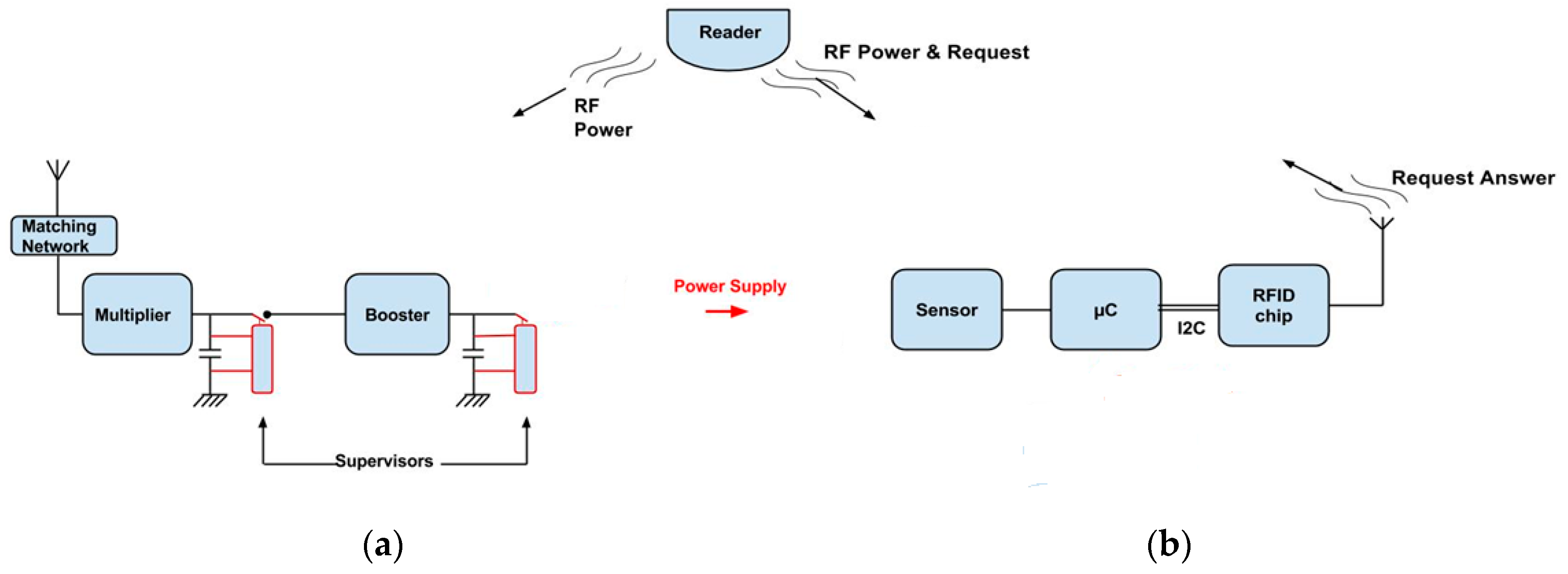
We separate the global architecture in two parts in function of their role. The first one is the connected measurement system. Its role is to measure and communicate with the UHF RFID reader. The second part is the energy harvesting and conditioning circuit. It is designed and optimised to supply the needed energy to the measurement circuit during the measurement and the result communication.
2.1. The Connected Measurement Circuit
As shown in Figure 1b, the connected measurement circuit is composed of an UHF RFID chip connected to the microcontroller via an I2C bus. The sensor is connected and managed by an ultra-low power microcontroller. The energy remotely provided by the reader is sufficient for the RFID chip but not enough to activate the sensor and the microcontroller. Last low power microcontrollers have start voltage around 1.8 V. That is why we designed an RF energy harvesting and conditioning circuit, introduced in the next subsection, to provide the needed energy.
2.2. The RF Energy Harvesting and Conditioning Circuit
The harvesting circuit is presented in Figure 1a. It consists in an antenna, a matching network, a multiplier which rectifies and multiplies the signal, a first charge capacitor with its supervisor, a DC-DC boost converter to multiply continuous voltage and a second charge capacitor coupled with a supervisor. The key elements of our harvester circuit design are the supervisors. We present their functioning principle in the Section 3.
3. Efficiency Optimisation of the RF Energy Harvesting Circuit
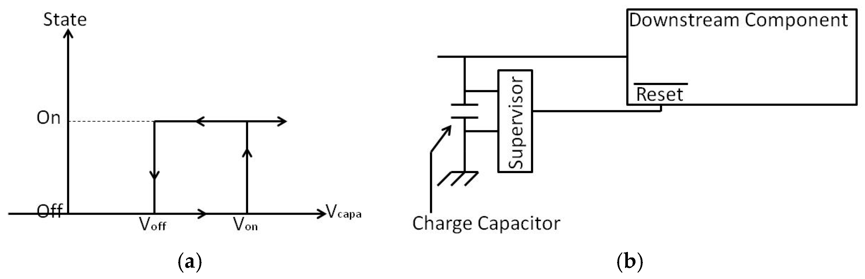
3.1. Presentation of the Supervisor Functioning
In our energy harvesting system, the supervisors play a key role regarding the efficiency optimisation: it control the use of the harvested energy. Indeed, the main difficulty is to get enough power to overpass the needed energy to activate the following stage. The supervisor turns off the downstream circuit and leaves time to the charge capacitor to reach the necessary voltage Von to activate the downstream component. Thanks to this, we prevent the system from ending up in an intermediary state, where the downstream component would drain energy from the capacitor—the latter’s voltage Vcapa thus remaining too low for the former to start. When the capacitor voltage drops below a minimum value Voff < Von, the supervisor turns off the downstream components. This hysteresis principle is shown in Figure 2a while Figure 2b presents the charge capacitor and supervisor coupled system.
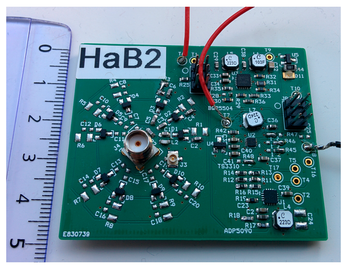
3.2. Prototype Circuit of the Energy Havesting System
For the measurement campaign, we realised a circuit prototype, presented in Figure 3 and composed of:
- LC matching network
- Multiplier stage with Schottky diodes
- Three different DC-DC boost converters for comparison
- Charge capacitors with supervisors
The multiplier stage and its LC matching network have been characterized first using electromagnetic simulation to determine the best configuration and component values. Then they have been adjusted experimentally.
The three boosters on the board are the AD5090, TS3310 and BQ25570. We choose the TS3310 because of its performances and it has the lower price.
The output voltage target is set to 2.1 V—which is representative of the start voltage of a measurement circuit such as we use.
4. Results and Discussion
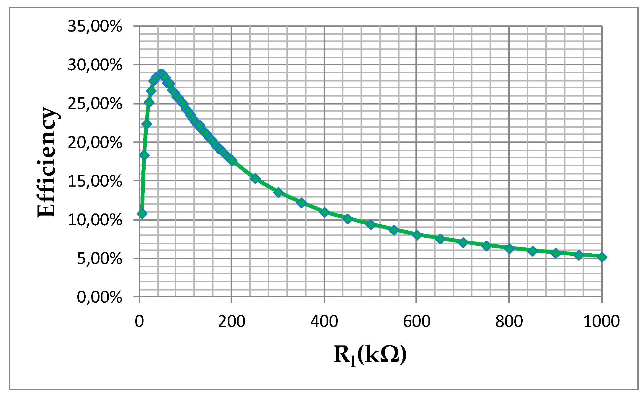
The multiplier stage is composed of four stages in the modified Greinacher configuration [1]. Its efficiency depending on the charge load is presented in Figure 4. Compared to the state of the art, this multiplier presents better performances [2,3,4].
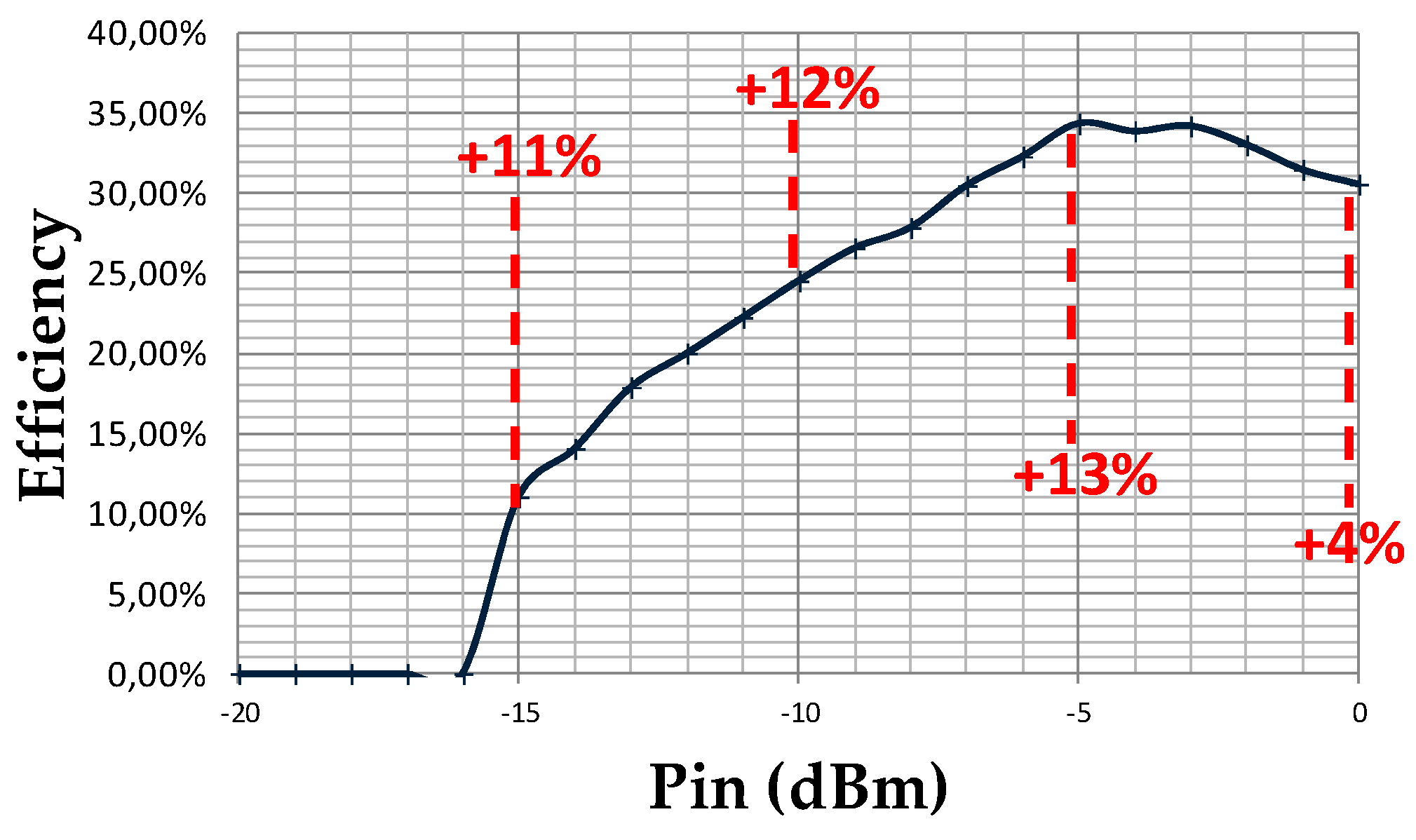
The overall system efficiency is presented in the Figure 6. With −10 dBm, we are able to obtain an efficiency of 25% which is an improvement of 10% compared to the same circuit without supervisors. Comparing with [5], where a similar configuration is used, but with only one supervisor, the efficiency for −10 dBm is about 21% since our system has a higher efficiency. Thanks to this enhanced system, we are able to obtain the 2.1 V required to activate the microcontroller and more generally to supply the measurement circuit with less input power as shown in Figure 5. The minimum input power to activate the measurement circuit is reduced from −11 dBm to −15 dBm and the efficiency gain of our system is clearly improved in comparison with the same measure without supervisor.
5. Conclusions
In this paper, we presented our work on the design of a connected autonomous sensor and we particularly focus on the use of supervisors in the energy harvesting circuit to optimise its sensitivity and efficiency. Thanks to supervisors, we are able to reach our target of 2.1 V with an input power of only −15 dBm. For −5 dBm input power, we obtain an efficiency of 35%. The next step of this work is to integrate this circuit with the measurement system (sensor and RFID UHF tag).
Conflicts of Interest
The authors declare no conflict of interest.
References
- Curty, J.-P.; Declercq, M.; Joehl, N.; Dehollain, C. Design and Optimization of Passive UHF RFID Systems; Springer: Boston, MA, USA, 2007. [Google Scholar]
- Shokrani, M.R.; Khoddam, M.; Hamidon, M.N.B.; Kamsani, N.A.; Rokhani, F.Z.; Shafie, S.B. An RF Energy Harvester System Using UHF Micropower CMOS Rectifier Based on a Diode Connected CMOS Transistor. Sci. World J. 2014, 2014, e963709. [Google Scholar] [CrossRef] [PubMed]
- Michelon, D.; Bergeret, E.; Di Giacomo, A.; Pannier, P. Optimization of integrated dickson voltage-multipliers for RF energy harvesting. In Proceedings of the IEEE 12th International New Circuits and Systems Conference (NEWCAS), Trois-Rivieres, QC, Canada, 22–25 June 2014; pp. 445–448. [Google Scholar]
- Chaour, I.; Bdiri, S.; Fakhfakh, A.; Kanoun, O. Modified rectifier circuit for high efficiency and low power RF energy harvester. In Proceedings of the 13th International Multi-Conference on Systems, Signals Devices (SSD), Leipzig, Germany, 21–24 March 2016; pp. 619–623. [Google Scholar]
- De Donno, D.; Catarinucci, L.; Tarricone, L. An UHF RFID Energy-Harvesting System Enhanced by a DC-DC Charge Pump in Silicon-on-Insulator Technology. IEEE Microw. Wirel. Compon. Lett. 2013, 23, 315–317. [Google Scholar] [CrossRef]
Figure 1.
Block diagram of the autonomous connected sensor: (a) Block diagram of the RF energy harvesting and conditioning circuit enhanced with supervisors coupled with charge capacitors; (b) Block diagram of the connected measurement system and UHF RFID reader on the top of the figure.
Figure 1.
Block diagram of the autonomous connected sensor: (a) Block diagram of the RF energy harvesting and conditioning circuit enhanced with supervisors coupled with charge capacitors; (b) Block diagram of the connected measurement system and UHF RFID reader on the top of the figure.

Figure 2.
Functional description of the charge capacitor and supervisor coupled system: (a) downstream component state versus charge capacity voltage value Vcapa; (b) diagram of the system.
Figure 2.
Functional description of the charge capacitor and supervisor coupled system: (a) downstream component state versus charge capacity voltage value Vcapa; (b) diagram of the system.

Figure 3.
Circuit prototype of the RF energy harvesting system.

Figure 4.
Multiplier efficiency with −10 dBm input power versus Rl load.

Figure 5.
Enhanced system efficiency and the added gain efficiency with supervisors versus input power.
Figure 5.
Enhanced system efficiency and the added gain efficiency with supervisors versus input power.

Publisher’s Note: MDPI stays neutral with regard to jurisdictional claims in published maps and institutional affiliations. |
© 2017 by the authors. Licensee MDPI, Basel, Switzerland. This article is an open access article distributed under the terms and conditions of the Creative Commons Attribution (CC BY) license (https://creativecommons.org/licenses/by/4.0/).
Share and Cite
MDPI and ACS Style
Safraou, A.; Bacot, P.; Dudret, S.; Bourdel, E.; Granado, B. RF Harvesting Circuit for Batteryless Connected Sensor. Proceedings 2017, 1, 583. https://doi.org/10.3390/proceedings1040583
AMA Style
Safraou A, Bacot P, Dudret S, Bourdel E, Granado B. RF Harvesting Circuit for Batteryless Connected Sensor. Proceedings. 2017; 1(4):583. https://doi.org/10.3390/proceedings1040583
Chicago/Turabian StyleSafraou, Ahcine, Patrick Bacot, Stéphane Dudret, Emmanuelle Bourdel, and Bertrand Granado. 2017. "RF Harvesting Circuit for Batteryless Connected Sensor" Proceedings 1, no. 4: 583. https://doi.org/10.3390/proceedings1040583