Uniform Fabrication of Moems Arrays Using Dry Thick Resist Films †

Abstract
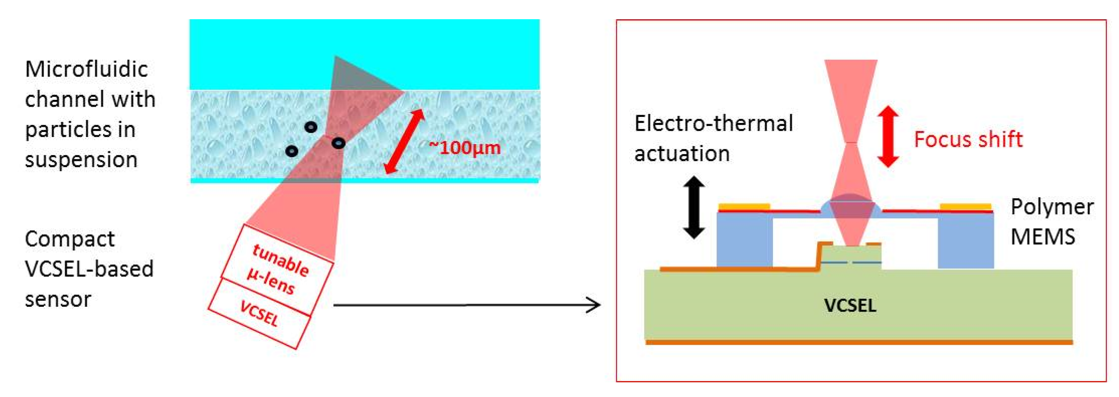
:1. Introduction
2. Materials and Methods
2.1. Design
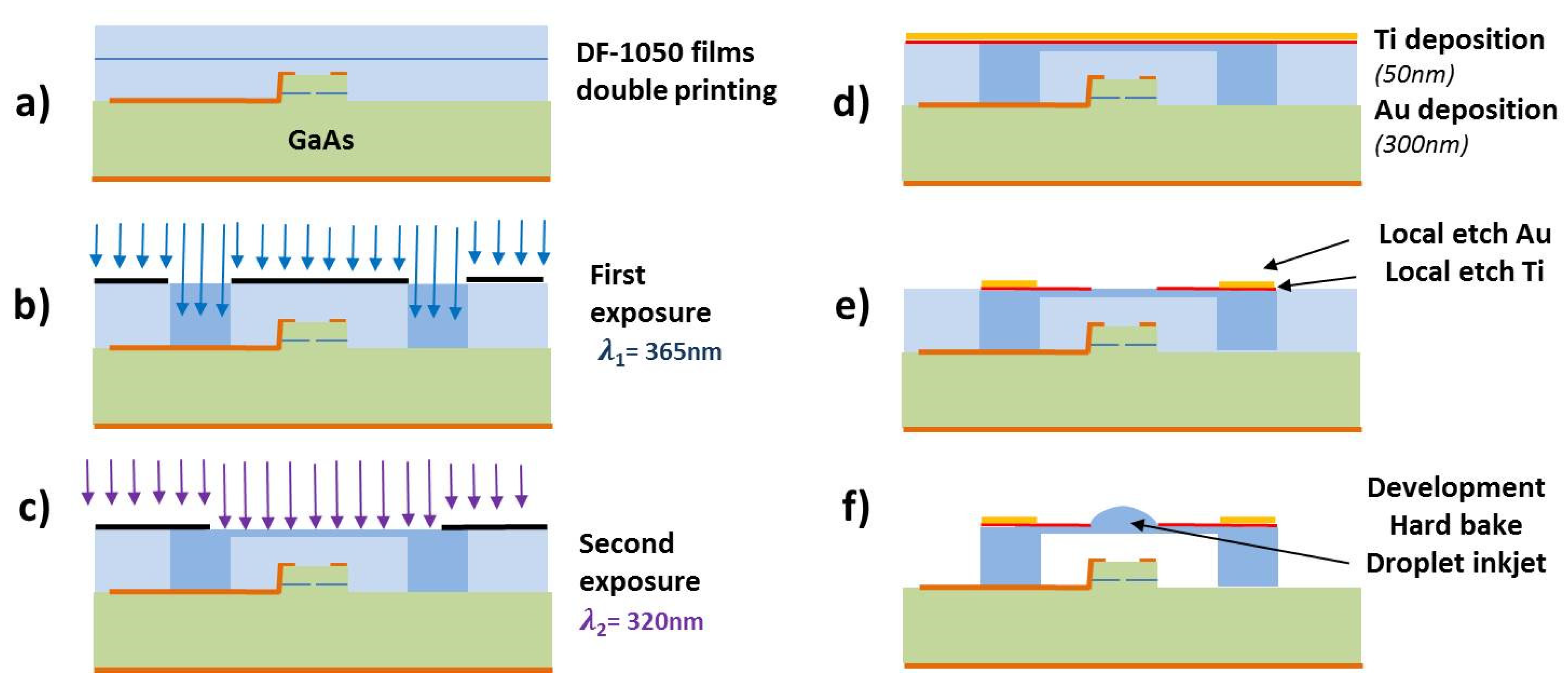
2.2. Fabrication
3. Results and Conclusions
Acknowledgments
Conflicts of Interest
References
- Reig, B.; Camps, T.; Bardinal, V.; Bourrier, D.; Daran, E.; Doucet, J.B.; Launay, J.; Fourniols, J.Y. Fabrication of polymer-based optical microsystem arrays suited for the active focusing of vertical laser diodes. J. Micromech. Microeng. 2012, 22, 065006. [Google Scholar] [CrossRef]
- Zhao, Y.; Julien, P.; Lucie, C.; Thierry, C.; Reza, A.; Véronique, B. Optical feedback interferometry for microscale−flow sensing study: Numerical simulation and experimental validation. Opt. Express 2016, 24, 23849–23862. [Google Scholar] [CrossRef] [PubMed]
- Abada, S.; Camps, T.; Reig, B.; Doucet, J.B.; Daran, E.; Bardinal, V. 3D optimization of a polymer MOEMS for active focusing of VCSEL beam. Proc. SPIE 2014, 913003. [Google Scholar] [CrossRef]
- Courson, R.; Cargou, S.; Conédéra, V.; Fouet, M.; Blatché, C.; Serpentini, C.L.; Gué, A.-M. Low-cost multilevel microchannel lab on chip: DF-1000 series dry film photoresist as a promising enabler. Advances, Royal Soc. Chem. 2014, 4, 54847–54853. [Google Scholar] [CrossRef]
- Abada, S.; Salvi, L.; Courson, R.; Daran, E.; Reig, B.; Doucet, J.B.; Camps, T.; Bardinal, V. Comparative study of soft thermal printing and lamination of dry thick photoresist films for the uniform fabrication of polymer MOEMS on small-sized samples. J. Micromech. Microeng. 2017, 27, 055018. [Google Scholar] [CrossRef]


Publisher’s Note: MDPI stays neutral with regard to jurisdictional claims in published maps and institutional affiliations. |
© 2017 by the authors. Licensee MDPI, Basel, Switzerland. This article is an open access article distributed under the terms and conditions of the Creative Commons Attribution (CC BY) license (https://creativecommons.org/licenses/by/4.0/).
Share and Cite
Camps, T.; Abada, S.; Reig, B.; Doucet, J.-B.; Courson, R.; Salvi, L.; Boisnard, B.; Daran, E.; Bardinal, V. Uniform Fabrication of Moems Arrays Using Dry Thick Resist Films. Proceedings 2017, 1, 551. https://doi.org/10.3390/proceedings1040551
Camps T, Abada S, Reig B, Doucet J-B, Courson R, Salvi L, Boisnard B, Daran E, Bardinal V. Uniform Fabrication of Moems Arrays Using Dry Thick Resist Films. Proceedings. 2017; 1(4):551. https://doi.org/10.3390/proceedings1040551
Chicago/Turabian StyleCamps, Thierry, Sami Abada, Benjamin Reig, Jean-Baptiste Doucet, Rémi Courson, Laurène Salvi, Benjamin Boisnard, Emmanuelle Daran, and Véronique Bardinal. 2017. "Uniform Fabrication of Moems Arrays Using Dry Thick Resist Films" Proceedings 1, no. 4: 551. https://doi.org/10.3390/proceedings1040551