Proceeding Paper

On the Development of Label-Free DNA Sensor Using Silicon Nanonet Field-Effect Transistors †

1
University Grenoble Alpes, CNRS, Grenoble INP ‡, LMGP, F-38000 Grenoble, France
2
University Grenoble Alpes, CNRS, Grenoble INP ‡, IMEP-LaHC, F-38000 Grenoble, France
3
University Grenoble Alpes, CNRS, LTM, F-38000 Grenoble, France
*
Author to whom correspondence should be addressed.
Presented at the Eurosensors 2017 Conference, Paris, France, 3–6 September 2017.
Proceedings 2017, 1(4), 312; https://doi.org/10.3390/proceedings1040312
Published: 28 August 2017
(This article belongs to the Proceedings of Proceedings of Eurosensors 2017, Paris, France, 3–6 September 2017)

Abstract

:
In this paper, the process and electrical characteristics of DNA sensor devices based on silicon nanonet (SiNN) field-effect transistors are reported. The SiNN, another name of randomly oriented Si nanowires network, was successfully integrated into transistor as p-type channel using standard microelectronic technology. The SiNN-based transistors exhibit a high initial ON-state current (5.10−8 A) and homogeneous electrical characteristics. For DNA detection, a new and eco-friendly functionalization process based on glycidyloxypropyltrimethoxysilane (GOPS) was performed which enables the covalent grafting of DNA probes on SiNN. This hybridization leads to a significant decrease of ON-state current of device. Additionally, it is observed that SiNN devices reveal reproductive current response to DNA detection. We demonstrate, for the first time, the successful integration of SiNN into sensor for electrical label-free DNA detection at low cost.

1. Introduction

The integration of silicon nanowire (SiNW) as electrical field-based sensors has been demonstrated as ultra-sensitive devices for label-free biomolecular detection [1]. However, the mass production of SiNW devices remains an ongoing challenge due to not only expensive technology but also lack of reproducibility in electrical properties from one NW device to another. To overcome this issue, we have proposed a new electrical field-based sensor using randomly deposited SiNW network, called nanonets (for Nanostructured Networks). The latter has shown interesting properties including not only high specific surface area but also tolerance to defects, thus, better reproductivity in physical properties as compared to NW [2,3,4]. Additionally, the electrical conductance of NN induces a promising electrical performance when integrated into field-based sensor as active element. Another remarkable property of NN is that they can be readily functionalized by attaching various functional groups on their surface, providing new properties to NN in view of biomolecule detection [4,5]. Such functionalized NN, with its intrinsic properties, opens a new opportunity to biosensing applications, notably DNA sensors.
Covalent grafting of DNA probes on Si based substrates starts usually with a silanization step using an organosilane. Aminopropyltriethoxysilane (APTES) [4] and GOPS [6] have been studied in our group. In the present study, the GOPS-based silanization, which enables faster and direct grafting of DNA as compared to APTES process, is used. Electrical behavior of sensors before and after DNA hybridization are reported in the following part.

2. Results and Discussion

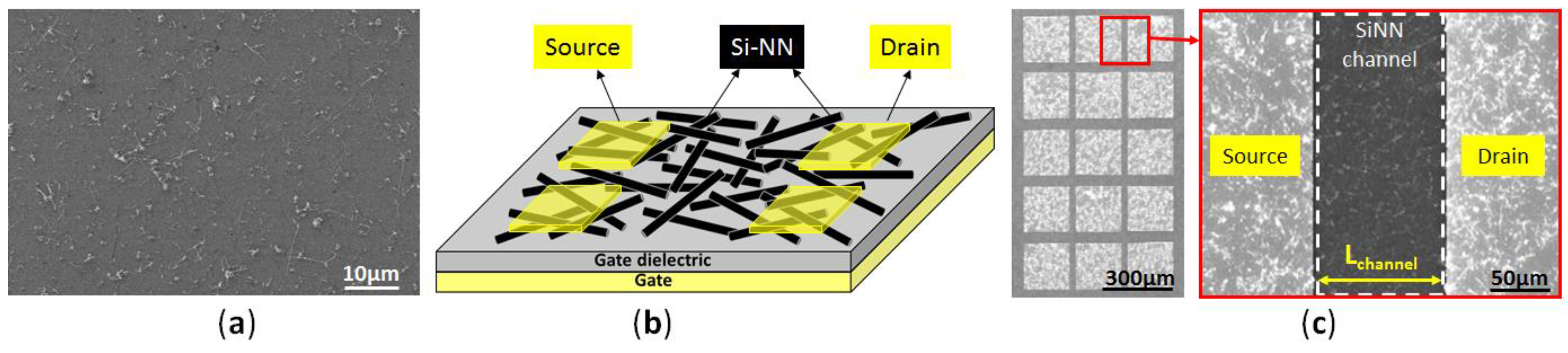
2.1. From Nanonet Formation to Functional NN-Based Field-Effect Transistors (FET)

The silicon nanowires, with average diameter and length of 40 nm and 7 μm respectively, were synthesized and detailed previously [2,7]. After growth, SiNWs were dispersed by sonication into deionized water for 5 min. 28 mL of such NW suspension was then filtered in vacuum through a nitrocellulose membrane forming nanonets with a density of 6.5 × 10⁷ (NWs·cm−2). For their integration into transistors, the elaborated NN was afterwards transferred onto 200-nm-thick Si3N4 on heavily doped silicon substrate by filter dissolution. Figure 1a shows the morphology of the NN after being transferred.
A homogeneous distribution of the NN on Si/Si3N4 substrate was observed, indicating successful NN transfer. This simple and efficient self-assembly process demonstrates undoubtedly its potential to a large-scale fabrication. After the transfer, the NN was sintered by rapid thermal annealing under nitrogen at 400 °C for 1 min to perform conducting path between NW/NW junctions which enhances NN conductivity [2]. The sintered-NN-based transistors with bottom gate configuration, as described in the Figure 1b, have been fabricated using standard microelectronic technology [7]. To define by lift-off the source and drain contacts, a multilayer consisting of 100-nm-thick nickel and 50-nm-thick gold was deposited by evaporation. These devices were then annealed at 400 °C for 1 minute in order to promote the silicidation between Ni and NWs, thus, a good contact between semiconductor and electrodes.
The channel length of SiNN FET, defined as the distance between source and drain contact, as shown in the Figure 1c, was taken into account during device characterization. Transistor with channel shorter or equal to the NW length (7 μm) was considered as multi-parallel NWs device because holes could flow from source to drain without crossing a NW/NW junction. On the other hand, one with channel larger than 7 μm, where holes should pass through several NW/NW junctions, was considered as NN-based.

2.2. Electrical Characterization of SiNN FETs before Functionalization

Electrical characterization of SiNN-based FETs was performed using a typical probe station in which we can apply needed voltage to device electrodes, which in turn makes current appear in transistor channel. Here, we report only transfer characteristic of device which represents the channel current (Ids) versus voltage applied to transistor gate (Vgs). Figure 2 displays the Ids-Vgs curve at Vds equal −4 V of ten as-fabricated FETs (e.g., before functionalization) with 15-μm-channel-length.
As one can see from Figure 2, the device shows p-type channel operation. It exhibits high current in the ON-state (ON-state current), in the range of 5.10−8 A at Vgs = −25 V. Additionally, an ON/OFF current ratio as large as 103 was reached. An almost-homogeneous electrical characteristics of devices having similar channel length (15 μm) was observed, demonstrating the promising reproducibility in NN-based device performance [7,8].

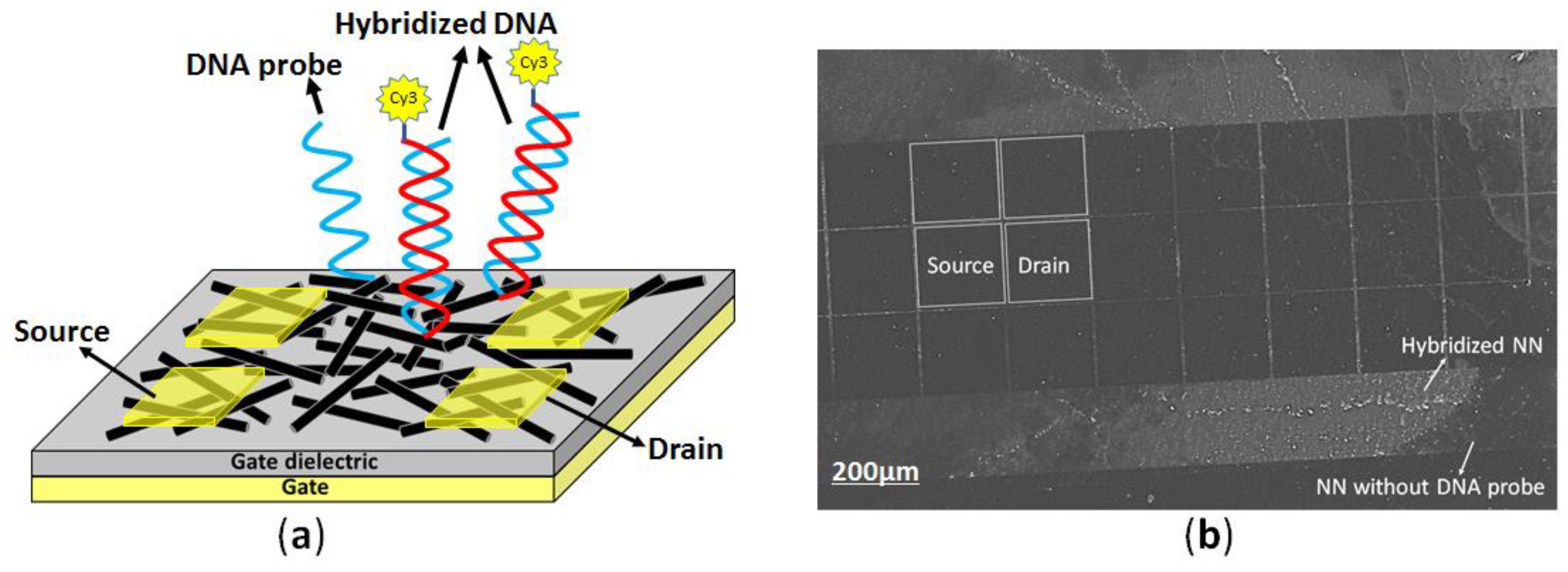
2.3. Functionalization Process of NN-Based Device for DNA Detection

For DNA detection, SiNN devices have been functionalized using GOPS. The process, including four steps: hydroxylation, silanization, DNA probe grafting, and DNA target hybridization, is detailed elsewhere [6]. Briefly the silanization is defined by depositing GOPS in vapor phase. This step enables direct grafting of DNA probe onto SiNN, as illustrated in the Figure 3a. As compared to commonly used APTES-based process, our process does not need the cross-linking step such as glutaraldehyde, thus, time-gain. Additionally, we have supposed that using GOPS brings the DNA chains closer to the NN surface, which enhances the response-time of sensor. In order to validate such DNA hybridization, fluorescent DNA targets were used. Figure 3b displays an observation of hybridized SiNN under fluorescent microscope.
This observation confirms the presence of DNA target on NN functionalized with probes and hence the hybridization. We report in the following section the electrical behavior of these sensors before and after DNA hybridization.

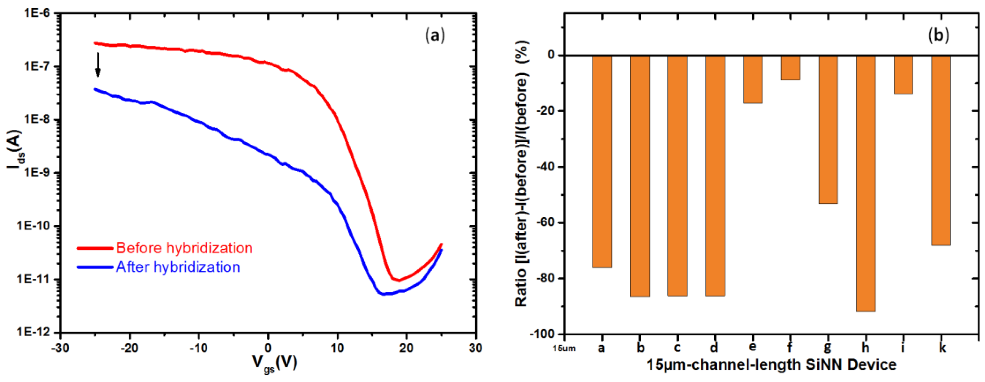
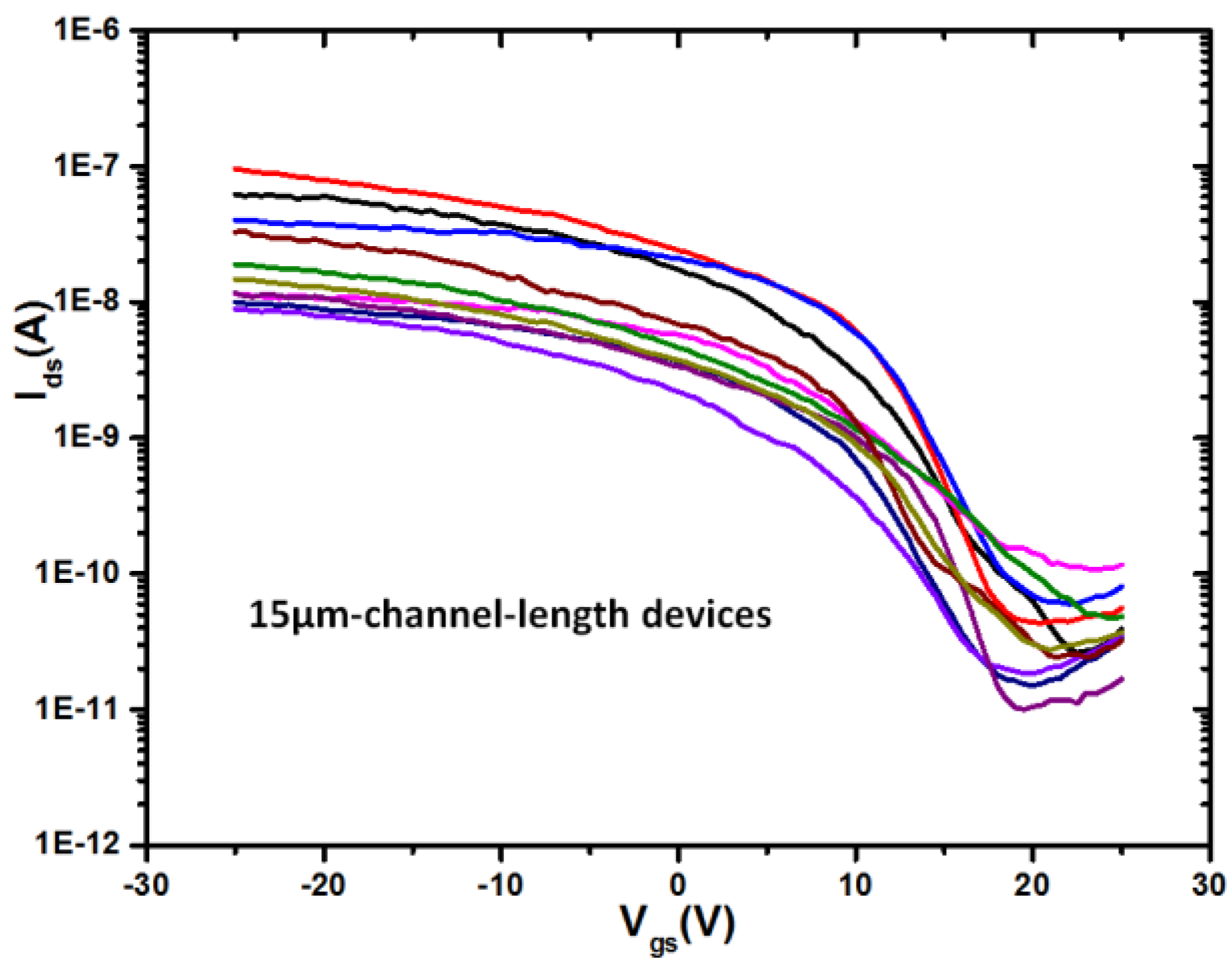
2.4. Electrical Characterization of SiNN-Based DNA Sensor

Figure 4a represents the transfer characteristic modification of SiNN transistor before and after hybridization. A significant current decrease after hybridization has been observed confirming double strand DNA detection. It can be reported, from Figure 4b, that the DNA sensors based-on SiNN reveal homogeneous characteristics and reproductive tendency of current response. The above results emphasize the potential of our SiNN technology for biosensor.

3. Conclusions

The first successful integration of SiNN into DNA sensor devices using standard microelectronic processes has been reported. The devices exhibit interesting properties such as a high ON-state current also a good ON/OFF ratio. DNA target hybridization leads to a significant decrease in ON-state current of device. Additionally, a reproductive current response to DNA detection was achieved. We demonstrate, for the first time, the successful integration of SiNN into sensor for electrical label-free DNA detection.

Acknowledgments

This work has received funding from the EU H2020 RIA project Nanonets2Sense under grant agreement No. 688329.

Conflicts of Interest

The authors declare no conflict of interest.

References

  1. Noor, M.O.; Krull, U.J. Silicon nanowires as field-effect transducers for biosensor development: A review. Anal. Chim. Acta 2014, 825, 1–25. [Google Scholar] [CrossRef] [PubMed]
  2. Ternon, C. Serre, P.; Lebrun, J.M.; Brouzet, V.; Legallais, M.; David, S.; Missiaen, J.M. Low Temperature Processing to Form Oxidation Insensitive Electrical Contact at Silicon Nanowire/Nanowire Junctions. Adv. Electron. Mater. 2015, 1, 10. [Google Scholar]
  3. Ternon, C.; Serre, P.; Rey, G.; Holtzinger, C.; Periwal, P.; Martin, M.; Langlet, M. High aspect ratio semiconducting nanostructure random networks: Highly versatile materials for multiple applications. Phys. Status Solidi Rapid Res. Lett. 2013, 7, 919–923. [Google Scholar] [CrossRef]
  4. Serre, P.; Ternon, C.; Stambouli, V.; Periwal, P.; Baron, T. Fabrication of silicon nanowire networks for biological sensing. Sens. Actuators B Chem. 2013, 182, 390–395. [Google Scholar] [CrossRef]
  5. Serre, P.; Stambouli, V.; Weidenhaupt, M.; Baron, T.; Ternon, C. Silicon nanonets for biological sensing applications with enhanced optical detection ability. Biosens. Bioelectron. 2015, 68, 336–342. [Google Scholar] [CrossRef] [PubMed]
  6. Demes-Causse, T.; Morisot, F.; Legallais, M.; Calais, A.; Pernot, E.; Pignot-Paintrand, I.; Ternon, C.; Stambouli, V. DNA grafting on silicon nanonets using an eco-friendly functionalization process based on epoxy silane. Materials Today Proceedings 2018. to be published. [Google Scholar]
  7. Legallais, M.; Nguyen, T.T.T.; Mouis, M.; Salem, B.; Ternon, C. Toward the integration of Si nanonets into FETs for biosensing applications. In Proceedings of the 2017 Joint International EUROSOI Workshop and International Conference on Ultimate Integration on Silicon (EUROSOI-ULIS), Athens, Greece, 3–5 April 2017. [Google Scholar]
  8. Cazimajou, T.; Legallais, M.; Mouis, M.; Ternon, C.; Salem, B.; Ghibaudo, G. Electrical Characterization of Percolating Silicon Nanonet FETs for sensing applications. In Proceedings of the 2017 Joint International EUROSOI Workshop and International Conference on Ultimate Integration on Silicon (EUROSOI-ULIS), Athens, Greece, 3–5 April 2017. [Google Scholar]
Figure 1. (a) SEM image of silicon nanonets elaborated from 28 mL of NW suspension; (b) Bottom configuration of SiNN FET; (c) SEM image of as-fabricated SiNN FET.
Proceedings 01 00312 g001
Figure 2. Transfer characteristic of ten as-fabricated SiNN FET with 15-μm-channel-length.
Proceedings 01 00312 g002
Figure 3. (a) SiNN FET with single and double strand DNA; (b) Fluorescent image of hybridized SiNN FET.
Proceedings 01 00312 g003
Figure 4. (a) Electrical response of SiNN FET before and after hybridization; (b) ON-state current ratio of ten 15 μm-channel-length SiNN FETs before and after hybridization, the letter refers to the measured FET.
Proceedings 01 00312 g004

