1. Introduction
This work has the intention to give a contribution towards the establishment of nanosphere lift-off lithography (NSLL) as an industrial manufacturing method for advanced nano-optoelectronic, nano-electronic, and nano-mechanical sensing devices based on vertical 3-dimensional gallium nitride (3D GaN) nanostructures. NSLL, as a special method of the colloidal lithography (CL), relies on using colloidal crystals to generate single-layer hexagonally spheres as masks for metallic vapor deposition or e-beam evaporation. It allows nanopattering of semiconductor substrates in a low-cost, high-throughput and large fabrication area process and consequently represents a good alternative to the sophisticated but expensive nanolithography methods, e.g., holographic lithography, electron beam lithography or ion beam lithography, since they are complicated, time consuming, and low-throughput processes for small areas. Thus, several attempts have been done in the last decades to optimize process parameters, diversify the patterns by changing the incident angle, and synthesize new homogeneous colloidal crystals materials with nanosize diameters [
1,
2]. However, almost all known studies were focused on silicon as semiconductor substrate for nanostructure fabrication [
2]. There are only few studies, which have examined the usability of NSLL for GaN substrates so far [
3]. Therefore, in this work, an alternative top-down nanofabrication approach combining NSLL and a new hybrid etching method has been carefully studied and utilized to fabricate vertically aligned 3D GaN nanowire arrays with diameters of <50 nm.
2. Nanofabrication Process and Results
The proposed nanofabrication comprises eight sequential processing steps starting from cleaning of the GaN wafers, which has been grown by metal-organic chemical vapour deposition (MOCVD) [
4], to the smoothening of the GaN nanowire sidewalls and reduction of the nanowire diameters by wet chemical etching. The whole process sequence is shown in
Figure 1.
At the beginning of the fabrication process, the chemical surface behavior had to be defined in terms of reproducibility of experiments and the following surface treatment processes. Therefore, a careful cleaning process was performed by boiling the untreated GaN substrate in isopropyl alcohol, incinerating organic compounds by O
2+ plasma cleaning, and finally removing all occurred oxides with buffered hydrofluoric acid (HF). After ensuring a clean substrate surface, 100 × 100 µm
2 photoresist microgrids were constructed to define selective area for deposition of the polystyrene nanobeads (PNs) (
Figure 1b). The photoresist microgrids were intended to keep the beads close together and prevent a shift of the PNs by centrifugal force during the spin coating. To avoid a multilayer formation of the PNs, the height of the photoresist microgrids has to be adjusted to the PN diameter by varying the rotational speed of the spin coater and the concentration of the photoresist, which should be kept between a half and a full NP diameter. The hydrophilicity of the substrate has a significant impact on the contact behavior between the GaN surface and the aqueous polystyrene suspension. To enhance the wetting capability of the GaN substrate, polyanion PSS (Poly(styrolsulfonate)) and polycation PDDA (Poly(diallyldimethylammonium chloride) were deposited using layer-by-layer (LbL) assembly technique (
Figure 2), which leads to a reduced contact angle of 32°, compared to untreated surface (49°).
After functionalizing the GaN surface, the self-assembly of PNs was initiated due to nucleation and crystal growth by performing two spin coating steps. For this, the aqueous polystyrene suspension was dripped on the hydrophilic GaN surface and sedimentation after the DLVO (Derjaguin, Landau, Verwey, Overbeek)-theory has to be awaited [
2]. After sedimentation, the first and slower (200 rpm) spin-coating step changed the surface tension of water surrounding the NPs and creates a lateral capillary force between the PNs. The second step (600 rpm) provided a convective nanoparticle flow towards the nucleus through the evaporation of the water, which resulted in a well arranged hexagonal close packed formation of PNs (
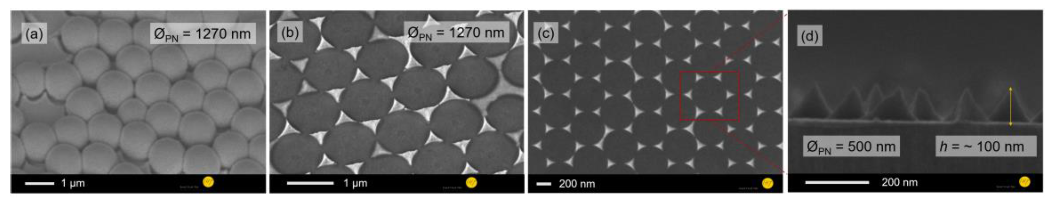
Figure 1d). An additional third spin-coating step (5200 rpm) was needed to remove the rest of the water and the humidity. The optimized process leads to PN distribution of ~35%, which could be used as a lift-off layer to define equidistant triangles of chromium dry etching masks. Therefore, an e-beam evaporation process was performed to define a 300 nm chromium layer over the whole substrate (
Figure 3a). Subsequently, the chromium covered PNs were removed in an ethanol ultrasonic bath, leaving the equidistant triangles in the PN interstices with bow-tie like arrangement (
Figure 3b,c). A 90° SEM image shows the remaining pyramidal chromium mask shape (
Figure 3d).
In contrast to commonly used Cl
2-based GaN dry etching, the nanowires were fabricated in a hybrid top-down approach combining ICP-DRIE etching with SF
6/H
2 gases and KOH-based wet chemical etching [
5,
6]. The ICP-DRIE process was performed with the following initial recipe: an ICP power of 800 W, an HF power of 275 W, SF
6 and H
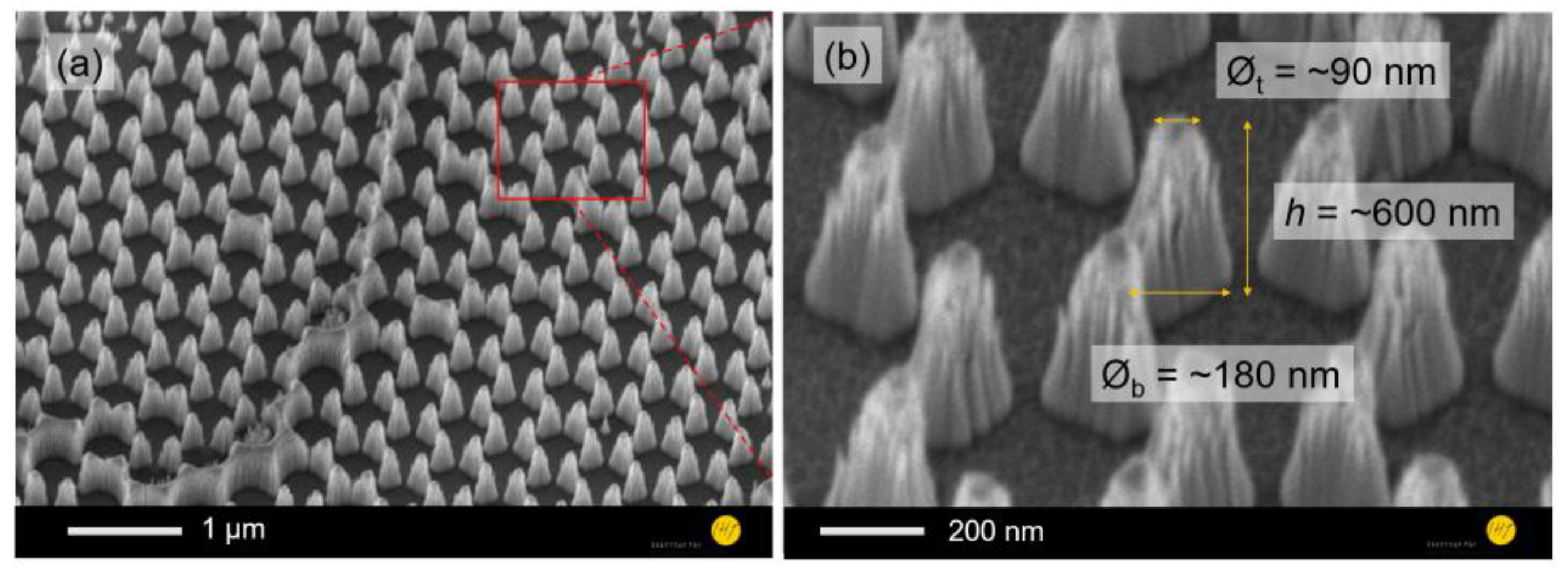
2 flow rates of 12 and 100 sccm, respectively, a pressure of 1 Pa, and at room temperature. Because of the strong physical impact of the dry etching process, the high-energy ion bombardment attacked the GaN wafer surface and caused heavily rugged sidewalls (
Figure 4), which however could be easily removed by a following KOH-based wet chemical etching process due to the ICP induced defects. After the relatively fast smoothing of the rugged sidewalls non-polar, the chemical stable crystal facets of GaN nanowire could occur, which leads to a lower etching rate and the capability to control the nanowire diameter precisely by adjustment of the etching time [
5]. The wet etching process was performed in an oil bath with an AZ 400 K developer as etchant and at ~80 °C. Therefore, vertical GaN nanowire arrays with diameter of ~35 nm, pitch of ~350 nm, and aspect ratio of >10 could finally be realized, although some defects were still pronounced (
Figure 5).
3. Conclusions
The proposed nanofabrication process allows the low-cost and high-throughput production of vertically aligned 3D GaN nanowire arrays with diameters down to 35 nm and pitch of ~350 nm. The diameter of the nanowires is precisely controllable by wet etching time, while the pitch depends completely on the PN diameter. Therefore, a further reduction of the pitch stays in contrast to a high aspect ratio, since the height of triangular chromium etching mask, which protects the substrate against the ion bombardment, is also correlated to the NP diameter. However, the quality of the colloidal crystal mask is the most important factor for the NSLL process and monocrystalline colloidal crystals with a large area still have not been yet obtained and thus needs precisely controlled conditions. An upcoming approach to enhance the self-assembly process of growing high-quality colloidal crystals is a further optimization of the wetting capabilities by varying the concentration of the PSS and PDDA solutions. A higher concentration of the polystyrene-nanoparticle solution could also have positive impact on the homogeneity of the PN mask. In addition, the influence of different microgrid shapes and sizes will be examined.

 ,
, 


