Porous Silicon Carbide for MEMS †


Institute of Sensor and Actuator Systems, TU Wien, Gusshausstrasse 27-29, 1040 Vienna, Austria
*
Author to whom correspondence should be addressed.
†
Presented at the Eurosensors 2017 Conference, Paris, France, 3–6 September 2017.
Proceedings 2017, 1(4), 297; https://doi.org/10.3390/proceedings1040297
Published: 30 August 2017
(This article belongs to the Proceedings of Proceedings of Eurosensors 2017, Paris, France, 3–6 September 2017)
Abstract
:Metal assisted photochemical etching (MAPCE) of 4H Silicon Carbide (SiC) was utilized to generate locally defined porous areas on single crystalline substrates. Therefore, Platinum (Pt) was sputter deposited on 4H-SiC substrates and patterned with photolithography and lift off. Etching was performed by immersing the Pt coated samples into an etching solution containing sodium persulphate and hydrofluoric acid. UV light irradiation was necessary for charge carrier generation while the Pt served as local cathode. The generated porous areas can be used for the generation of integrated cavities in the single crystalline SiC substrates when covered with a chemical vapor deposited thin film of poly-crystalline SiC.
1. Introduction
Porous semiconductors are a popular topic in research and development, with porous silicon (pSi) as the most prominent representative. When pSi is annealed at temperatures up to 1100 °C it reorganizes to minimize surface energy. This effect is utilized in the fabrication of pressure sensors by the formation of cavities after high temperature annealing [1]. Furthermore, the separation of thin single crystalline silicon layers is possible [2]. Because of the chemical inertness, mechanical stability and high band gap of SiC, MEMS devices based on this wide band gap semiconductor can be operated at higher temperatures and in more aggressive environments than devices fabricated in standard silicon micromachining. Furthermore, thin SiC layers are most beneficial for UV detectors. For the realization of novel device concepts, the tailored porosification in selected areas of mono-crystalline SiC substrates is regarded as a key technology.
Porous SiC (pSiC) can be prepared by metal assisted photochemical etching (MAPCE), which in contrast to conventional anodization of SiC, is capable of producing uniform porous layers. In this approach a noble metal like Platinum (Pt) is deposited on the SiC surface, serving as local cathode. When the sample is immersed in an etching solution containing an oxidizing agent and hydrofluoric acid, a charge transfer occurs with electrons flowing from the SiC substrate via the Pt/SiC interface to the etching solution. Simultaneously pSiC forms at the bare SiC surface. Recent experiments showed that reliable etching can be achieved by decreasing the contact resistance at the Pt/SiC junction [3].
In this paper MAPCE is utilized to generate locally defined pSiC which is necessary for the realization of device concepts mentioned above.
2. Materials and Methods
For the experiments square sized samples (1 × 1 cm2) were cut from single crystalline 4H-SiC wafers with different resistivities of 0.02 and 0.106 Ω·cm. Then the samples were cleaned consecutively with acetone and ethanol. The samples having a resistivity of 0.106 Ω·cm were surface near doped with a diffusion based approach utilizing a phosphoric acid solution and high temperatures up to 1100 °C. This was done to decrease the contact resistance during etching at the Pt/SiC interface. The experimental details can be found elsewhere [3]. After cleaning, 10% of the sample’s surface were covered with 300 nm Pt by sputter deposition. Next the samples were annealed for 5 min under Argon flow at 1100 °C with a prior temperature ramp starting at 800 °C that lasted for 30 min. This was done to further decrease the contact resistance at the Pt/SiC interface. [3] After this annealing step, 100 nm Pt were again sputter deposited and structured with photolithography and lift off. This was done because the annealing and doping processes lead to surface roughening. By the chosen two-step process, structuring of the samples could be done at smooth parts of the samples. Finally the samples were immersed in an etching solution containing 0.04 mol/L sodium persulphate and 1.31 mol/L hydrofluoric acid (HF). In the case of samples with a resistivity of 0.02 Ω·cm 1.2 mL of etching solution were used while a custom built 18 W UVC source was used for irradiation. For samples with higher resistivity, 150 mL of etching solution were used while a 250 Watt ES280LL mercury arc lamp at full spectrum was applied for irradiation. After etching for 2 h the Pt was removed with boiling aqua regia and polycrystalline SiC was deposited with a hot wall low pressure chemical vapor deposition (LPCVD) furnace from FirstNano®. The SiC films were deposited at 1050 °C using gas flows of 1sccm SiH4 and 60 sccm CH4 with 500 sccm H2 as background gas.
3. Discussion
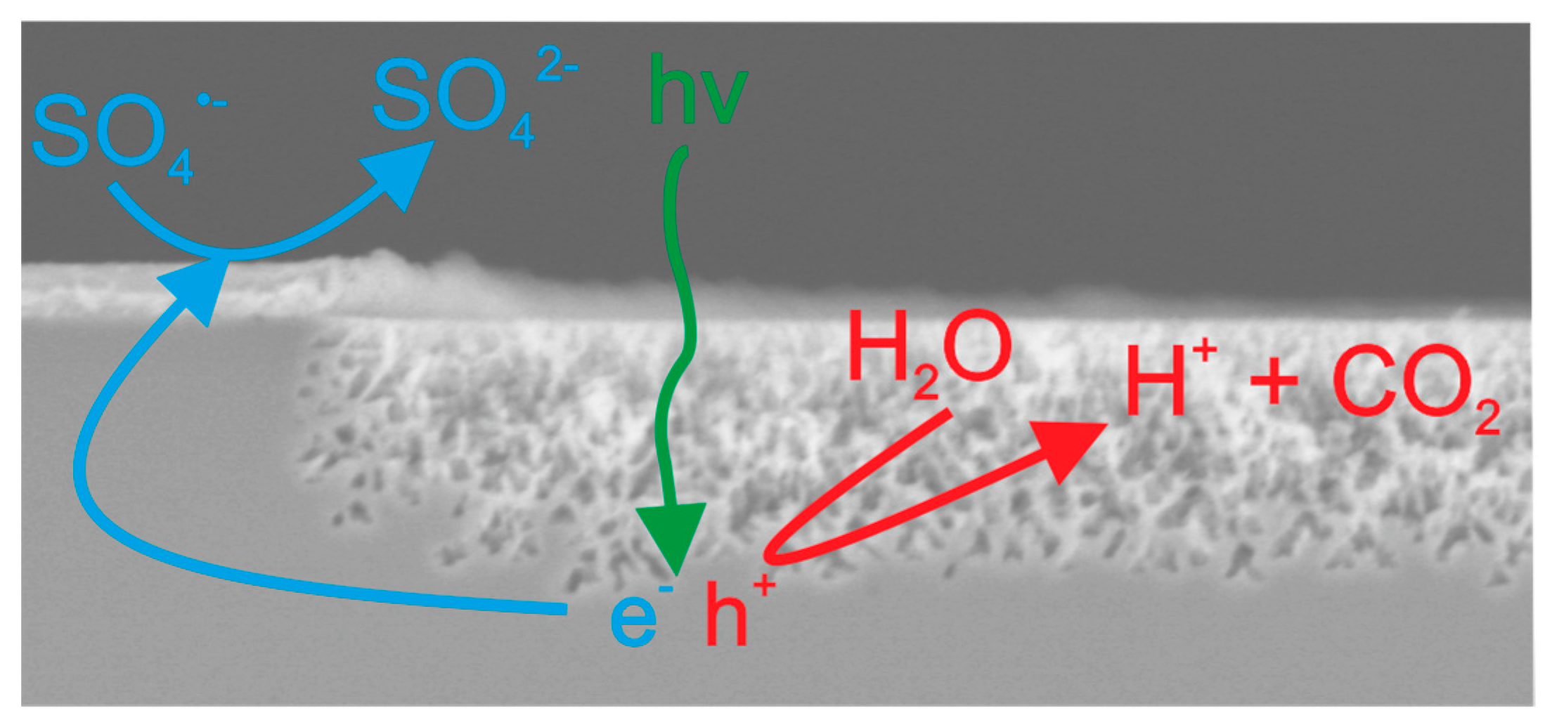
During etching porous layers were generated at the bare SiC surface which had not been covered with Pt. This is illustrated in Figure 1. One can see a secondary electron microscope (SEM) micrograph showing pSiC and the schematically indicated charge carrier flow paths during etching. UV light generates charge carries (electrons e−, holes h+). The holes, together with H2O are responsible for the oxidation of SiC, while the oxide is afterwards dissolved by HF leaving behind pSiC. To restore charge neutrality during etching, the electrons are accepted from the oxidizing agent (SO4−) at the Pt/etching solution interface [3].
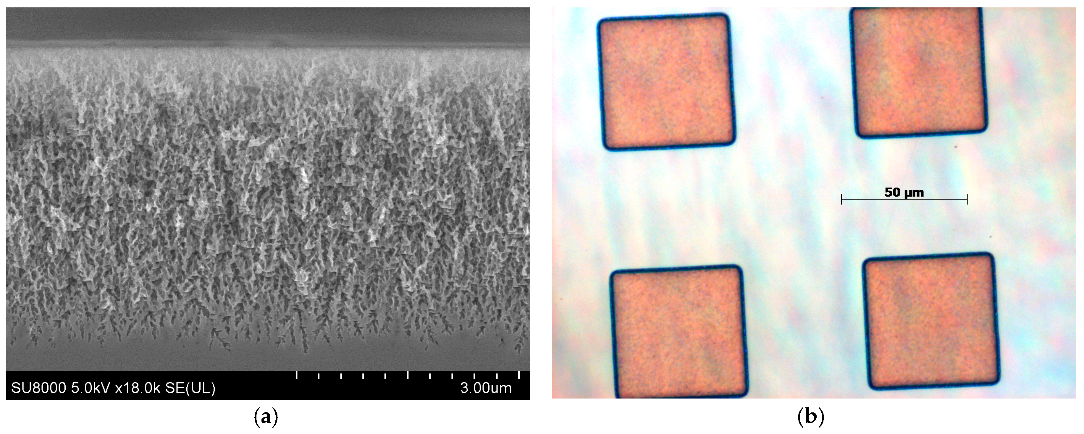
For successful application of the generated pSiC layers, the Pt cathodes have to be removed completely after MAPCE without damaging or dissolving the pSiC. This was possible with aqua regia, as is shown in Figure 2 (sample resistivity of 0.106 Ω·cm). One can see that the pSiC remains intact after removing the Pt with boiling aqua regia (see Figure 2a). A corresponding top down view (see Figure 2b) shows that it is possible to locally define pSiC on single crystalline substrates. The orange areas show pSiC which is surrounded by dense SiC.
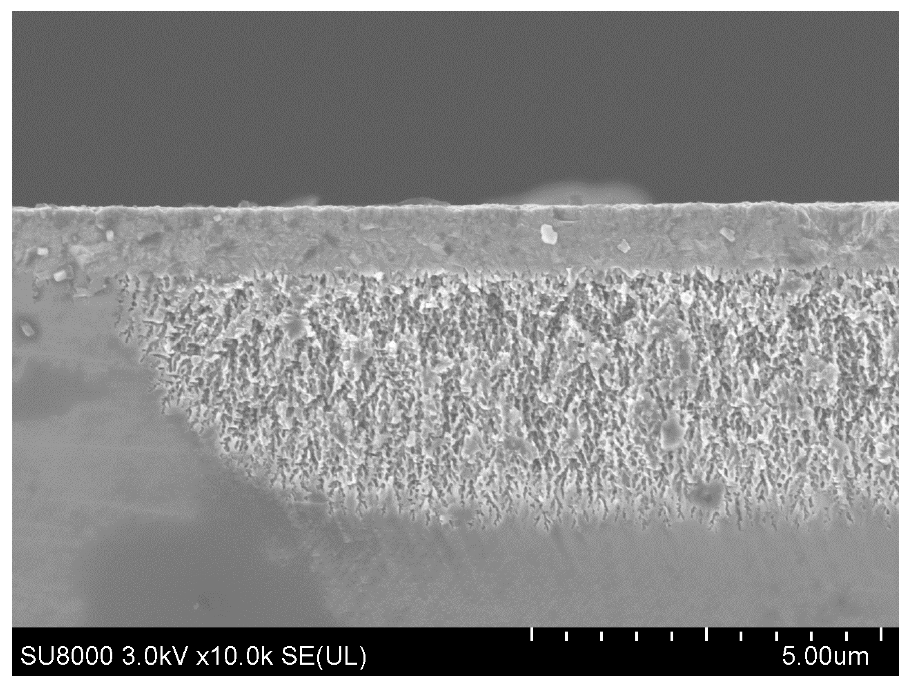
Many possible application scenarios, such as the layer transfer method or epitaxial growth of GaN [4], require the deposition of thin films via CVD without filling the porous material. This could in principle be shown with a sample having a resistivity of 0.106 Ω·cm, as is illustrated in Figure 3. It can be seen that a pSiC area is covered with polycrystalline SiC, while the porous layer was not re-filled with polycrystalline SiC.
Another possible application scenario of the process described so far is the formation of cavities for e.g., pressure sensor fabrication as demonstrated by Armbruster et al. for pSi [1]. In this approach pSi reorganizes under high temperatures leaving behind a cavity covered with a membrane on top. This membrane is used for pressure sensor applications.
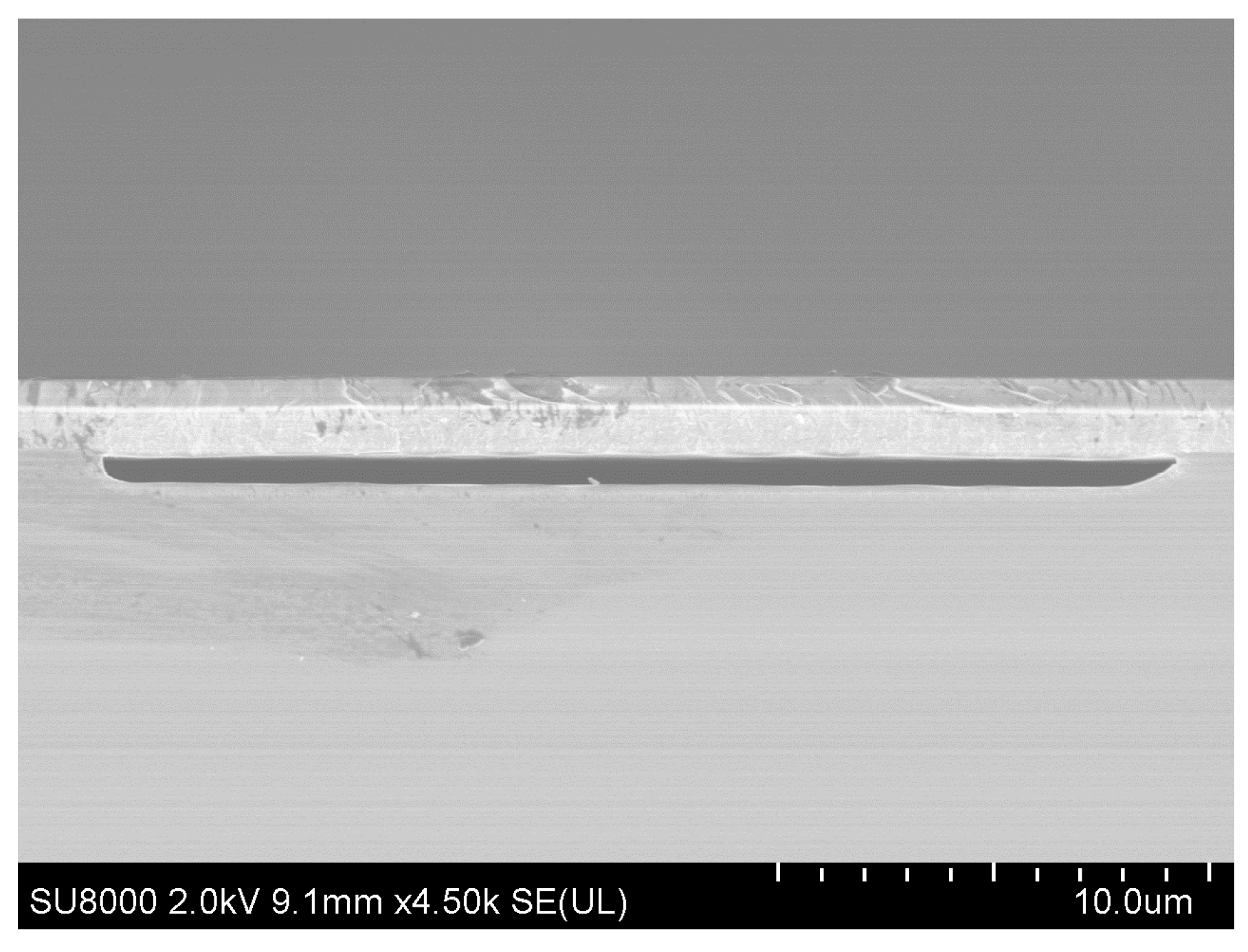
This approach is also possible for SiC substrates by utilizing MAPCE. Samples annealed at 1500 °C in air showed reorganization of the pSiC as is shown in Figure 4. A cavity has formed with polycrystalline SiC on top and single crystalline 4H SiC at the bottom. This sample had a resistivity of 0.02 Ω·cm. Besides the successful reorganization of pSiC it was also possible to use a low power UV source and a small amount of etchant for samples with lower resistivities (see experimental details). This is explained with a lower resistance for electron transport through the bulk SiC material during etching and is of economical as well as practical importance when toxic etching solutions are used.
In summary it can be stated that pSiC can be reliably generated with MAPCE and the presented results demonstrate the potential of this process for the realization of SiC-based MEMS/NEMS devices.
Acknowledgments
This project has been supported by the COMET K1 centre ASSIC Austrian Smart Systems Integration Research Center. The COMET—Competence Centers for Excellent Technologies—Programme is supported by BMVIT, BMWFW and the federal provinces of Carinthia and Styria.
Conflicts of Interest
The authors declare no conflict of interest.
References
- Armbruster, S.; Schafer, F.; Lammel, G.; Artmann, H.; Schelling, C.; Benzel, H.; Finkbeiner, S.; Larmer, F.; Ruther, R.; Paul, O. A novel micromachining process for the fabrication of monocrystalline Si-membranes using porous silicon. In Proceedings of the TRANSDUCERS, Solid-State Sensors, Actuators and Microsystems International Conference, 2003; pp. 246–249. [Google Scholar]
- Terheiden, B.; Hensen, J.; Wolf, A.; Horbelt, R.; Plagwitz, H.; Brendel, R. Layer Transfer from Chemically Etched 150 mm Porous Si Substrates. Materials 2011, 4, 941–951. [Google Scholar] [CrossRef] [PubMed]
- Leitgeb, M.; Backes, A.; Zellner, C.; Schneider, M.; Schmid, U. Communication—The Role of the Metal-Semiconductor Junction in Pt-Assisted Photochemical Etching of Silicon Carbide. ECS J. Solid State Sci. Technol. 2016, 5, P148–P150. [Google Scholar] [CrossRef]
- Inoki, C.K.; Kuan, T.S.; Sagar, A.; Lee, C.D.; Feenstra, R.M.; Koleske, D.D.; Diaz, D.J.; Bohn, P.W.; Adesida, I. Growth of GaN on porous SiC and GaN substrates. Phys. Status Solidi A 2003, 200, 44–47. [Google Scholar] [CrossRef]
Figure 1.
Schematic depiction of the mechanism of MAPCE.

Figure 2.
Porous SiC generated with MAPCE after Pt removal with aqua regia; (a) Cross sectional SEM micrograph; (b) Top down view optical microscope image. The orange areas indicate regions of pSiC surrounded by dense SiC.
Figure 2.
Porous SiC generated with MAPCE after Pt removal with aqua regia; (a) Cross sectional SEM micrograph; (b) Top down view optical microscope image. The orange areas indicate regions of pSiC surrounded by dense SiC.

Figure 3.
Porous silicon carbide covered with a polycrystalline SiC layer deposited with LPCVD.

Figure 4.
A micromachined cavity with bulk 4H-SiC at the bottom and polycrystalline SiC on top. As the annealing step was performed in air an oxide layers has formed on the poly-SiC membrane.
Figure 4.
A micromachined cavity with bulk 4H-SiC at the bottom and polycrystalline SiC on top. As the annealing step was performed in air an oxide layers has formed on the poly-SiC membrane.

Publisher’s Note: MDPI stays neutral with regard to jurisdictional claims in published maps and institutional affiliations. |
© 2017 by the authors. Licensee MDPI, Basel, Switzerland. This article is an open access article distributed under the terms and conditions of the Creative Commons Attribution (CC BY) license (https://creativecommons.org/licenses/by/4.0/).
Share and Cite
MDPI and ACS Style
Leitgeb, M.; Zellner, C.; Pfusterschmied, G.; Schneider, M.; Schmid, U. Porous Silicon Carbide for MEMS. Proceedings 2017, 1, 297. https://doi.org/10.3390/proceedings1040297
AMA Style
Leitgeb M, Zellner C, Pfusterschmied G, Schneider M, Schmid U. Porous Silicon Carbide for MEMS. Proceedings. 2017; 1(4):297. https://doi.org/10.3390/proceedings1040297
Chicago/Turabian StyleLeitgeb, Markus, Christopher Zellner, Georg Pfusterschmied, Michael Schneider, and Ulrich Schmid. 2017. "Porous Silicon Carbide for MEMS" Proceedings 1, no. 4: 297. https://doi.org/10.3390/proceedings1040297