
Performance Study of Virtual Frisch Grid CdZnTeSe Detectors


1
Savannah River National Laboratory, Aiken, SC 29808, USA
2
Brookhaven National Laboratory, Upton, NY 11973, USA
*
Author to whom correspondence should be addressed.
Instruments 2022, 6(4), 69; https://doi.org/10.3390/instruments6040069
Submission received: 30 August 2022
/
Revised: 10 October 2022
/
Accepted: 21 October 2022
/
Published: 26 October 2022
Abstract
:Nuclear detectors for x-ray and gamma-ray spectroscopy and imaging are a vital tool in many homeland security, medical imaging, astrophysics and other applications. Most of these applications require room-temperature operation due to the operational constraints imposed by a cryogenic cooling system. CdZnTe (CZT) has been the main material with the desired detection properties, and CZT crystals have been used commercially for three decades. However, CdZnTe still suffers from long-standing issues of high densities of performance-limiting intrinsic defects such as Te inclusions and networks of dislocation walls (sub-grain boundaries). A recently invented new quaternary material CdZnTeSe showed excellent material properties for radiation detection. The material was found to be free from dislocation networks, possess reduced Te inclusions, and have better compositional homogeneity. Virtual Frisch grid detectors were fabricated from crystals taken from a CdZnTeSe ingot that was grown by the traveling heater method. The detectors were fabricated from an as-grown ingot, bypassing the post-growth annealing process commonly practiced for industrial-grade CZT. The performances of the detectors were studied with different Frisch grid lengths using an amplifier shaping time ranging from 1–6 µs. The detectors showed high-quality spectroscopic performance with an as-measured energy resolution of ~1.1% at 662 keV for an optimum Frisch grid length of 3 mm. The charge collection was observed to enhance for longer Frisch grids.
1. Introduction
The development of Cd1−xZnxTe (CZT) has been revolutionary in the semiconductor industry for X- and gamma-ray radiation detector applications. As a room temperature radiation detector material, CZT has proven to be instrumental for technological advances in radiological and nuclear detection, particularly for applications in the field where compact low-maintenance instruments are needed. CZT has been used for homeland security, non-proliferation, gamma telescopes, high energy physics, medical imaging, and other applications such as the mining industry [1,2,3,4,5,6,7]. As a result, the material has dominated the commercial market for more than three decades, although it still possesses several critical materials-related issues. The widespread deployment of detectors based on CZT, especially for large-volume devices, has been impaired due to the presence of high concentrations of intrinsic defects such as sub-grain boundary network and secondary phases (especially Te inclusions), which are known to be detrimental to detector performance [8,9,10,11]. The compositional inhomogeneity in CZT ingots is another major disadvantage of the material [12] because it compromises the overall yield of detector-grade crystals. The presence of high concentrations of these defects and compositional inhomogeneity eventually severely hampers the yield of high-quality detector materials and in turn increases the production cost of high-performance detectors. These defects are typically generated during the growth and subsequent cooling process. The reduction in these defects has proved to be non-trivial due to the poor thermo-physical properties of the material. Thus, the quest for a cost-effective alternative material is being actively pursued globally by the research community. Because of the stringent material properties essential for room-temperature operation, only a handful of materials have evolved as potential alternates to CZT. Thallium bromide (TlBr) has been considered as a strong contender to replace CZT [13,14,15,16]. However, after more than two decades of intense research, TlBr still shows unresolved issues of contact degradation and device polarization, and various approaches are being investigated in an attempt to resolve these issues [15,16]. In more recent years, cesium lead bromide (CsPbBr3) has become the most promising perovskite material for room-temperature nuclear detector applications [17,18]. However, ion migration and defects under an applied electric field affect the device stability over time [19]. Thus, achieving high-performance and low-cost for a semiconductor-based nuclear detector operable at room temperature continues to be a major challenge.
Historically, selenium has long been known as an effective lattice hardening element in the CdTe/CZT matrix, resulting in a drastic reduction of the dislocation density and sub-grain boundary network, as originally reported by the substrate community for night-vision applications [20,21,22,23,24]. Selenium-contained CdTe/CZT material was also found to have better compositional homogeneity compared to CZT [23,24]. To avail the advantages of adding selenium in CdTe/CZT, we developed CdxZn1−xTeySe1−y (CZTS) for radiation detector applications. The addition of selenium to the CZT matrix was found to have several advantages regarding the material properties and successfully mitigated most of the defects that are present in present-day CZT. The resulting quaternary material CZTS was observed to be free from sub-grain boundary networks with reduced density/smaller size of Te inclusions [25,26,27,28,29]. The CZTS ingots also possessed better compositional homogeneity for ingots grown by either the vertical Bridgman technique or traveling heater method (THM) [25,27,28,29]. In addition, the density of electrically active defects and trap states responsible for degradation of detector performances were also reduced as compared to CZT [30,31]. The mechanical hardness of the quaternary material was reported to be enhanced as compared to conventional CZT material [32]. Therefore, detectors based on CZTS have the potential to outperform CZT for both homeland security and medical imaging applications [27,31]. Because of the superior material properties compared to CZT, the new CZTS material quickly attracted attention by researchers, and it is currently under active research by several groups [31,33,34,35]. Very recently, another selenium-based new material CdMnTeSe has been explored for radiation detector applications [36].
After producing CZTS ingots with various compositions of selenium, the composition with 10 atomic % of Zn and 2 atomic % of Se was found to be the optimum for the best detector performance [37]. The band gap of CZTS was reported to decrease with increasing amount of selenium [22], and a lower bandgap has a detrimental effect on the leakage current and noise in operating devices. Hence, the concentration of selenium was optimized so that a minimum amount of selenium could be used to eliminate most sub-grain boundaries in CZTS and provide for a low concentration of Te inclusions. For the entire concentration range of selenium considered (1.5 at. % to 7 at. %), the material was found to be free from sub-grain boundary networks. High concentrations of Te inclusions were observed in CZTS containing selenium at about 1.5 at. %, while CZTS containing 2–7 at. % of selenium showed very low concentration of Te inclusions. The charge transport properties were also found to be superior for Cd0.9Zn0.1Te0.98Se0.02 as compared to other studied compositions, so this investigation focused on 2.0 at. % Se [37]. Here, we report the results of a study of the detector performance of an as-grown Cd0.9Zn0.1Te0.98Se0.02 crystal fabricated from an ingot grown by the THM technique.
2. Materials and Methods
Detectors with the virtual Frisch grid (VFG) geometry were fabricated from an as-grown two-inch diameter Cd0.9Zn0.1Te0.98Se0.02 ingot grown by the traveling heater method (THM). Bar-shaped VFG detectors employ a large geometrical aspect ratio. The end faces of each detector are metallized and serve as anode and cathode. The dark resistivity and electron mobility-lifetime product [(µτ)e] values of the Cd0.9Zn0.1Te0.98Se0.02 detector-grade material is in the range of 1–3 × 10¹⁰ ohm-cm, and 4–5 × 10⁻³ cm2/V, respectively. After cutting the desired size of the detector sample using a programmable diamond-impregnated wire saw, all sides of the sample are carefully lapped on successive grit size SiC paper. Care was taken to maintain all the sides of the sample perpendicular to each other. The sample was then successively polished in an alumina suspension with reduced particle sizes on a felt pad, and finally polished with 0.05-µm alumina suspension to a mirror-like finish.
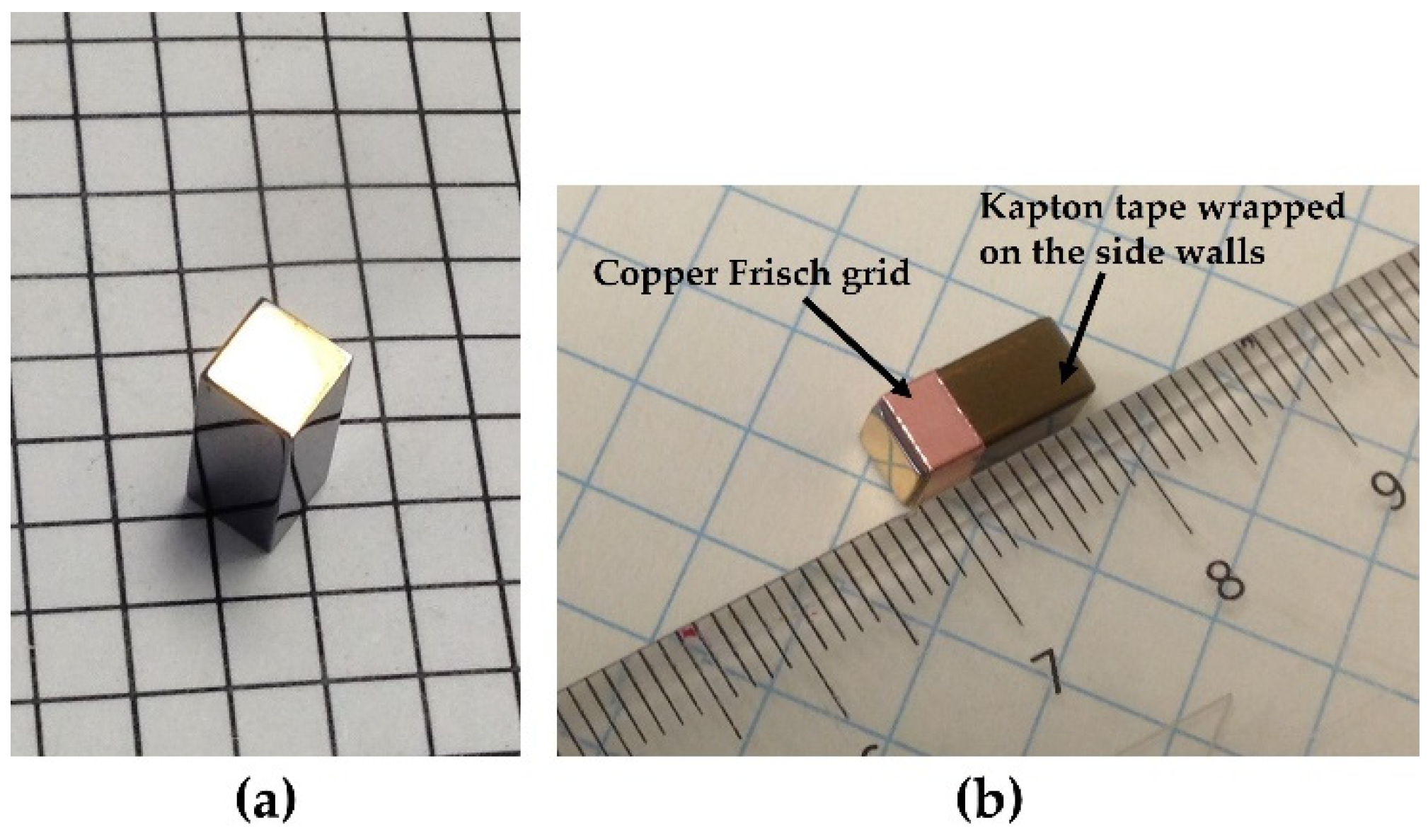
Bromine-methanol etching is a routine step for cleaning the surface prior to CZT electrode deposition process. The bromine-methanol etched surfaces are known to increase the dark current due to a higher surface leakage current. The higher surface current is caused by a residual Te-rich surface remaining after bromine-methanol etching of CdTe-based samples. Duff et al. [38] reported very high surface leakage current for 1% Br-methanol solution etched surface as compared to as-polished surfaces of CdZnTe detector. To reduce the thermal noise of the fabricated detector, we opted to fabricate the detector on as-polished surfaces. Figure 1a shows a typical virtual Frisch grid detector sample with gold contacts placed on the two ends of the detector. Gold contacts were deposited on the end faces using a gold chloride solution by the electroless deposition process. The VFG detector was assembled by wrapping the side walls of the detector sample with insulated Kapton tape, followed by wrapping with copper tape, which acts as the Frisch ring/grid as shown in Figure 1b. The cathode side was irradiated with the gamma source for all detector measurements. The Frisch grid ring and the cathode are electrically joined together and are connected to the ground of the detection system. The induced signal was measured through an eV Products A4039 preamplifier and an Ortec 672 shaping amplifier. A MCA-3 series/P 7882 card from FAST ComTec was used to register the spectra. The shaping time used for all the spectra was 2 or 3 µs. In this present study, detector performances were evaluated with different Frisch grid lengths between 2–8 mm. All the measurements were carried out at room temperature conditions of between 21–23 °C.
3. Results and Discussion
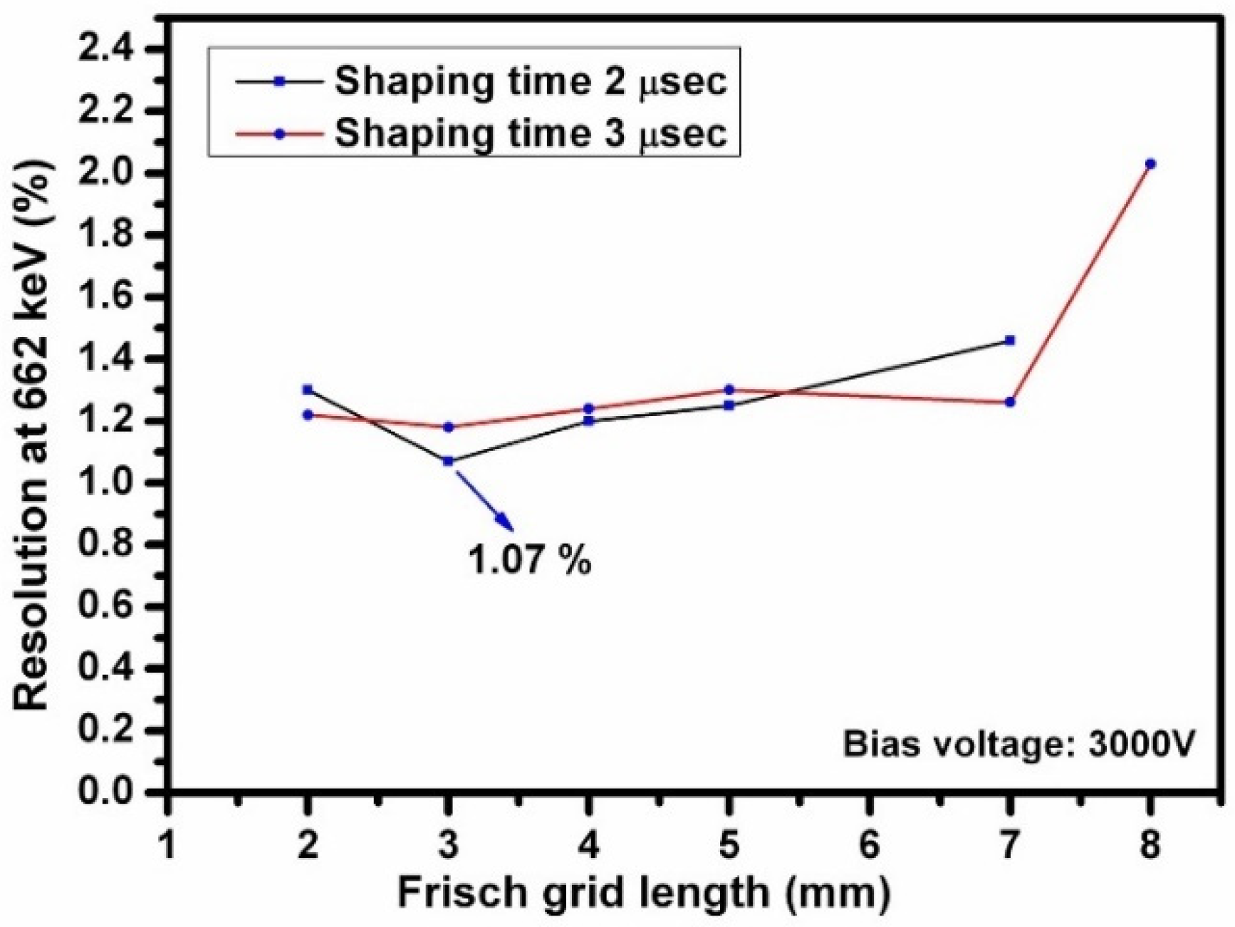
The performance of the detector was evaluated with an amplifier shaping time ranging from 1 µs to 6 µs for the Frisch grid length of 2–8 mm. The best energy resolution obtained was for the VFG detector with a 3-mm Frisch grid length and shaping time of 2 µs. The variation of the energy resolution at 662 keV from a 137Cs source with different Frisch grid lengths is shown in Figure 2 for an amplifier shaping time of 2 and 3 µs. The energy resolution at 662 keV was ~1.0 to 1.1% for the detector with a Frisch grid length of 3 mm and shaping time of 2 µs as shown in Figure 2. The applied operating bias was 3000 volts.
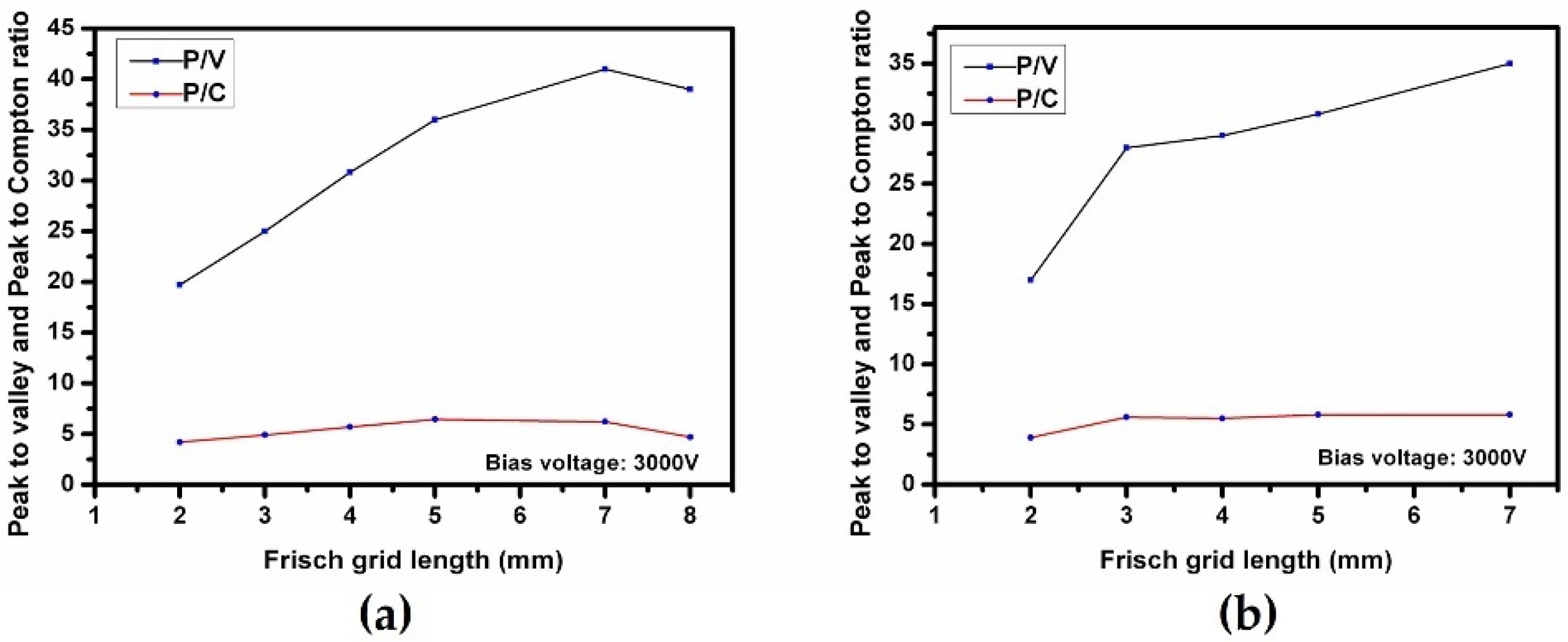
The Peak-to-Valley (P/V) ratio and Peak-to-Compton (P/C) ratio for the 662-keV pulse height spectra registered for the detector with different Frisch grid lengths (2 mm to 8 mm) for a 2 µs and 3 µs shaping time are illustrated in Figure 3 for an applied bias voltage of 3000 V. The Peak-to-Compton ratio (P/C) for both shaping times is observed to be almost constant for different Frisch grid lengths as shown in Figure 3, while the Peak-to-Valley ratio (P/V) was found to increase with the Frisch grid length. Similar behavior was also observed for large-volume CZTS based detectors with a size of ~2.3 cm3 [39]. Both the P/V and P/C ratios were reported to increase with the Frisch grid length for a CZT detector with a length of 14 mm [40]. The rate of the increase is reported to be high for the Frisch grid length up to 6 mm. For 6–12 mm long Frisch grids, the rate was more moderate [40]. An intrinsic photopeak efficiency was also reported for the CZT Frisch grid detector with increased Frisch grid length [40]. In the present case for CZTS, the sharp increase in P/V ratio for Frisch grid lengths up to 7 mm indicates increased charge collection in the photopeak, since the counts in the valley showed relatively little change for the range of Frisch grid lengths considered in this study. It is expected that an extension of the grid length up to near 10 mm (i.e., approximately the full thickness of the detector) will begin to cause a decrease in the P/V ratio and an increase in the width of the 662-keV photopeak.
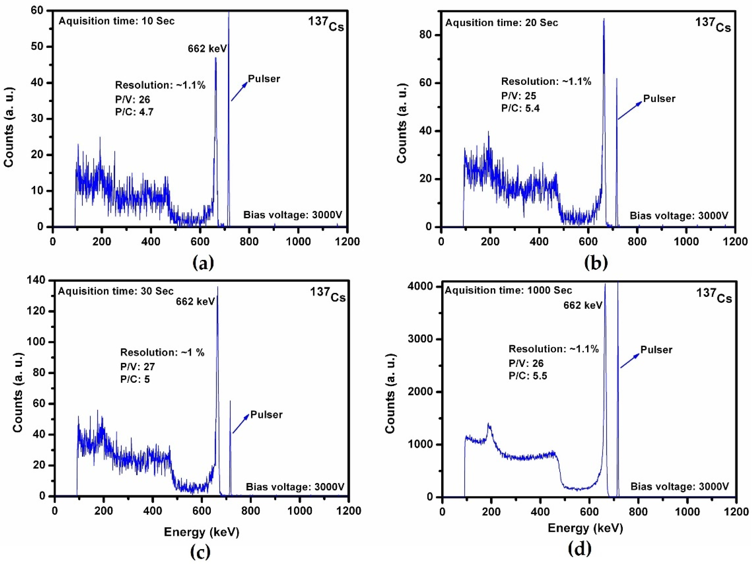
The detector performance was evaluated with different acquisition times while the detector was biased at 3000 V. The pulse height spectra acquired for different acquisition time at different time interval for the uncollimated 137Cs source is shown in Figure 4. The source was placed ~3 mm away from the cathode side of the detector. The shaping time used for all the detector response was 2 µs. Each spectrum was collected for a certain acquisition time, and after interval of 5–10 min, the second spectrum was collected for different acquisition time while the applied bias was kept constant at 3000 V. The pulse height spectra for acquisition times of 10, 20, 30 and 1000 s are shown in Figure 4a–d. The measured energy resolution of the 662-keV peak was ~1.0–1.1%. The peaks labeled as “pulser” show the electronic pulse, and the sharpness of the electronic pule indicates very low electronic noise of the device. It is important to note that all the pulse height spectra presented here are as-measured, and the device was fabricated from as-grown CZTS ingot. No post-growth annealing process was employed as opposed to the conventional route for CZT technology. The very well resolved peak in the spectrum with 10-s acquisition time illustrates the high sensitivity of the detector. No drift of the peak position (channel number) or degradation of the device performance was observed for different time interval and acquisition time, demonstrating that the detector is free from any charge polarizing effect. The pulse height is generally known to degrade and shift towards the lower channel with time under constant applied bias due to the polarization effect [41]. The CZTS-based detectors were very stable with time under the applied operating bias. The excellent energy resolution of the detector demonstrates the very high quality of the detector material. It is to be noted that for an energy resolution of ~1–2% at 662 keV for CZT devices, the required (µτ)e value should be in the range of 10−2 cm2/V. While for CZTS, energy resolution in the range of ~0.77–1.2% at 662 keV for ~10 mm long devices could be achieved for the moderate (µτ)e value of 4–6 × 10⁻³ cm2/V [27,42]. This also suggests superior material quality and uniformity with very low concentrations of performance-limiting defects present in CZTS as compared to the conventional CZT.
4. Conclusions
We have studied the performance of virtual Frisch grid detector fabricated from an as-grown Cd0.9Zn0.1Te0.98Se0.02 ingot grown by the traveling heater method. The device exhibited high energy-resolution with high sensitivity. Under an applied bias of 3000 volts, the device was found to be very stable over time. The superior energy resolution of ~1% at 662 keV at room temperature for ~10 mm-long detector with moderate (µτ)e value (4–6 × 10⁻³ cm2/V) for electrons indicates the high-quality nature of the CZTS material with very low concentrations of performance-limiting defects.
Author Contributions
U.N.R. and R.B.J. conceived the idea, and U.N.R. was the primary author of the manuscript text. U.N.R. and G.S.C. were involved in cutting, polishing and device fabrication. Y.C., G.S.C. and U.N.R. were involved in the detector measurements. R.B.J., U.N.R. and Y.C. were involved in the data analysis. All the authors participated in scientific discussions and critically reviewed the manuscript. All authors have read and agreed to the published version of the manuscript.
Funding
This work was partially supported by the U.S. Department of Energy, Office of Defense Nuclear Nonproliferation Research and Development, and the Laboratory Directed Research and Development (LDRD) program within the Savannah River National Laboratory (SRNL). This work was produced by Battelle Savannah River Alliance, LLC, under Contract No. 89303321CEM000080 with the U.S. Department of Energy. The publisher acknowledges the U.S. Government license to provide public access under the DOE Public Access Plan (http://energy.gov/downloads/doe-publicaccess-plan).
Data Availability Statement
The data that support the findings of this study are available from the corresponding author upon reasonable request.
Conflicts of Interest
The authors declare no conflict of interests.
References
- Schlesinger, T.E.; Toney, J.E.; Yoon, H.; Lee, E.Y.; Brunett, B.A.; Franks, L.; James, R.B. Cadmium zinc telluride and its use as a nuclear radiation detector material. Mater. Sci. Eng. R 2001, 32, 103–189. [Google Scholar] [CrossRef]
- Yang, G.; James, R.B. CdTe and Related Compounds; Physics, Defects, Hetero- and Nano-Structures, Crystal Growth, Surfaces and Applications Part II; Triboulet, R., Siffert, P., Eds.; Elsevier: Amsterdam, The Netherlands, 2009; pp. 214–238. [Google Scholar]
- Barthelmy, S.D.; Barbier, L.M.; Cummings, J.R.; Fenimore, E.E.; Gehrels, N.; Hullinger, D.; Krimm, H.A.; Markwardt, C.B.; Palmer, D.M.; Parsons, A.; et al. The burst alert telescope (BAT) on the SWIFT midex mission. Space Sci. Rev. 2005, 120, 143–164. [Google Scholar] [CrossRef] [Green Version]
- Krawczynski, H.S.; Stern, D.; Harrison, F.A.; Kislat, F.F.; Zajczyk, A.; Beilicke, M.; Hoormann, J.; Qingzhen, G.; Endsley, R.; Ingram, A.R.; et al. X-ray polarimetry with the Polarization Spectroscopic Telescope Array (PolSTAR). Astropart. Phys. 2016, 75, 8–28. [Google Scholar] [CrossRef] [Green Version]
- Slomka, P.J.; Miller, R.J.H.; Hu, L.H.; Germano, G.; Berman, D.S. Solid-State Detector SPECT Myocardial Perfusion Imaging. J. Nucl. Med. 2019, 60, 1194–1204. [Google Scholar] [CrossRef]
- Jing, W.; Chi, L. Recent advances in cardiac SPECT instrumentation and imaging methods. Phys. Med. Biol. 2019, 64, 06TR01. [Google Scholar]
- Santarelli, M.F.; Giovannetti, G.; Hartwig, V.; Celi, S.; Positano, V.; Landini, L. The Core of Medical Imaging: State of the Art and Perspectives on the Detectors. Electronics 2021, 10, 1642. [Google Scholar] [CrossRef]
- Carini, G.A.; Bolotnikov, A.E.; Camarda, G.S.; James, R.B. High-resolution X-ray mapping of CdZnTe detectors. Nucl. Instrum. Methods Phys. Res. A 2007, 579, 120–124. [Google Scholar] [CrossRef]
- Amman, M.; Lee, J.S.; Luke, P.N. Electron trapping nonuniformity in high-pressure-Bridgman-grown CdZnTe. J. Appl. Phys. 2002, 92, 3198–3206. [Google Scholar] [CrossRef] [Green Version]
- Bolotnikov, A.E.; Camarda, G.S.; Cui, Y.; Yang, G.; Hossain, A.; Kim, K.; James, R.B. Characterization and evaluation of extended defects in CZT crystals for gamma-ray detectors. J. Cryst. Growth 2013, 379, 46–56. [Google Scholar] [CrossRef]
- Awadalla, S.A.; Mackenzie, J.; Chen, H.; Redden, B.; Bindley, G.; Duff, M.C.; Burger, A.; Groza, M.; Buliga, V.; Bradley, J.P.; et al. Characterization of detector-grade CdZnTe crystals grown by traveling heater method (THM). J. Cryst. Growth 2010, 312, 507–513. [Google Scholar] [CrossRef]
- Zhang, N.; Yeckel, A.; Burger, A.; Cui, Y.; Lynn, K.G.; Derby, J.J. Anomalous segregation during electrodynamic gradient freeze growth of cadmium zinc telluride. J. Cryst. Growth 2011, 325, 10–19. [Google Scholar] [CrossRef]
- Hitomi, K.; Tada, T.; Onodera, T.; Kim, S.Y.; Xu, Y.; Shoji, T.; Ishii, K. TlBr Capacitive Frisch Grid Detectors. IEEE Trans. Nucl. Sci. 2013, 60, 1156–1161. [Google Scholar] [CrossRef]
- Datta, A.; Becla, P.; Motakef, S. Novel Electrodes and Engineered Interfaces for Halide-Semiconductor Radiation Detectors. Sci. Rep. 2019, 9, 9933. [Google Scholar] [CrossRef] [PubMed] [Green Version]
- Takagi, K.; Toyoda, K.; Kase, H.; Takagi, T.; Tabata, K.; Terao, T.; Morii, H.; Koike, A.; Aoki, T.; Nogami, M.; et al. Bias Polarity Switching-Type TlBr X-Ray Imager. IEEE Trans. Nucl. Sci. 2021, 68, 2435–2439. [Google Scholar] [CrossRef]
- Datta, A.; Fiala, J.; Becla, P.; Motakef, S. Stable room-temperature thallium bromide semiconductor radiation detectors. Appl. Phys. Lett. Mater. 2017, 5, 106109. [Google Scholar] [CrossRef] [Green Version]
- He, Y.; Matei, L.; Jung, H.J.; McCall, K.M.; Chen, M.; Stoumpos, C.C.; Liu, Z.; Peters, J.A.; Chung, D.Y.; Wessels, B.W.; et al. High spectral resolution of gamma-rays at room temperature by perovskite CsPbBr3 single crystals. Nat. Comm. 2018, 9, 1609. [Google Scholar] [CrossRef] [Green Version]
- He, Y.; Petryk, M.; Liu, Z.; Chica, D.G.; Hadar, I.; Leak, C.; Ke, W.; Spanopoulos, I.; Lin, W.; Chung, D.Y.; et al. CsPbBr3 perovskite detectors with 1.4% energy resolution for high-energy γ-rays. Nat. Photonics 2021, 15, 36–42. [Google Scholar] [CrossRef]
- Zhang, B.B.; Wang, F.; Zhang, H.; Xio, B.; Sun, Q.; Guo, J.; Hafsia, A.B.; Shao, A.; Xu, Y.; Zhou, J. Defect proliferation in CsPbBr3 crystal induced by ion migration. Appl. Phys. Lett. 2020, 116, 063505. [Google Scholar] [CrossRef]
- Rudolph, P. Fundamental studies on Bridgman growth of CdTe. Prog. Crystal Growth Charact. 1994, 29, 275–381. [Google Scholar] [CrossRef]
- Johnson, C.J. Recent progress in lattice matched substrates for HgCdTe epitaxy. SPIE Proc. 1989, 56, 1106. [Google Scholar]
- Brill, G.; Chen, Y.; Amritraj, P.M.; Sarney, W.; Chandlerhorowitz, D.; Dhar, N.K. Molecular beam epitaxial growth and characterization of Cd-based II–VI wide-bandgap compounds on Si substrates. J. Electron. Mat. 2005, 34, 655–661. [Google Scholar] [CrossRef]
- Tanaka, A.; Masa, Y.; Seto, S.; Kawasaki, T. Zinc and selenium co-doped CdTe substrates lattice matched to HgCdTe. J. Cryst. Growth 1989, 94, 166–170. [Google Scholar] [CrossRef]
- Chang, C.Y.; Tseng, B.H. Crystal growth of CdTe alloyed with Zn, Se and S. Mater. Sci. Eng. B 1997, 49, 1–4. [Google Scholar] [CrossRef]
- Roy, U.N.; Camarda, G.S.; Cui, Y.; Gul, R.; Hossain, A.; Yang, G.; Zazvorka, J.; Dedic, V.; Franc, J.; James, R.B. Role of selenium addition to CdZnTe matrix for room-temperature radiation detector applications. Sci. Rep. 2019, 9, 1620. [Google Scholar] [CrossRef] [PubMed] [Green Version]
- Kleppinger, J.W.; Chaudhuri, S.K.; Roy, U.N.; James, R.B.; Mandal, K.C. Growth of Cd0.9Zn0.1Te1–ySey Single Crystals for Room-Temperature Gamma Ray Detection. IEEE Trans. Nucl. Sci. 2021, 68, 2429–2434. [Google Scholar] [CrossRef]
- Roy, U.N.; Camarda, G.S.; Cui, Y.; Gul, R.; Yang, G.; Zazvorka, J.; Dedic, V.; Franc, J.; James, R.B. Evaluation of CdZnTeSe as a high-quality gamma-ray spectroscopic material with better compositional homogeneity and reduced defects. Sci. Rep. 2019, 9, 7303. [Google Scholar] [CrossRef] [Green Version]
- Herraiz, L.M.; Brana, A.F.; Plaza, J.L. Vertical Gradient Freeze Growth of two inches Cd1−xZnxTe1−ySey ingots with different Se content. J. Cryst. Growth 2021, 573, 126219. [Google Scholar]
- Hwang, S.; Yu, H.; Bolotnikov, A.E.; James, R.B.; Kim, K. Anomalous Te inclusion size and distribution in CdZnTeSe. IEEE Trans. Nucl. Sci. 2019, 66, 2329–2332. [Google Scholar] [CrossRef]
- Gul, R.; Roy, U.N.; Camarda, G.S.; Hossain, A.; Yang, G.; Vanier, P.; Lordi, V.; Varley, J.; James, R.B. A comparison of point defects in Cd1−xZnxTe1−ySey crystals grown by Bridgman and traveling heater methods. J. Appl. Phys. 2017, 121, 125705. [Google Scholar] [CrossRef]
- Yakimov, A.; Smith, D.; Choi, J.; Araujo, S. Growth and characterization of detector-grade CdZnTeSe by horizontal Bridgman technique. Proc. SPIE 2019, 11114, 111141N. [Google Scholar]
- Franc, J.; Moravec, P.; Dedic, V.; Roy, U.; Elhadidy, H.; Minarik, P.; Sima, V. Microhardness study of Cd1−x ZnxTe1-ySey crystals for X-ray and gamma ray detectors. Mater. Today Comm. 2020, 24, 101014. [Google Scholar]
- Park, B.; Kim, Y.; Seo, J.; Byun, J.; Dedic, V.; Franc, J.; Bolotnikov, A.E.; James, R.B.; Kim, K. Bandgap engineering of Cd1− xZnxTe1− ySey (0<x<0.27, 0<y<0.026). Nucl. Instrum. Methods Phys. Res. A 2022, 1036, 166836. [Google Scholar]
- Chaudhuri, S.K.; Kleppinger, J.W.; Karadavut, O.M.; Nag, R.; Mandal, K.C. Quaternary Semiconductor Cd1− xZnxTe1−ySey for High-Resolution, Room-Temperature Gamma-Ray Detection. Crystals 2021, 11, 827. [Google Scholar] [CrossRef]
- Znamenshchykov, Y.; Pashchenko, M.; Kononov, O.; Volobuev, V.; Kurbatov, D.; Opanasyuk, A. Effect of Thermal Annealing on the Structural and Substructural Properties of Cd1−xZnxTe1-ySey Thick Polycrystalline Films. In Proceedings of the IEEE 11th International Conference Nanomaterials: Applications & Properties (NAP), Odesa, Ukraine, 5–11 September 2021; pp. 1–4. [Google Scholar] [CrossRef]
- Byun, J.; Seo, J.; Seo, J.; Park, B. Growth and characterization of detector-grade CdMnTeSe. Nucl. Engr. Technol. 2022, in press. [CrossRef]
- Roy, U.N.; Camarda, G.S.; Cui, Y.; James, R.B. Optimization of selenium in CdZnTeSe quaternary compound for radiation detector applications. Appl. Phys. Lett. 2021, 118, 152101. [Google Scholar] [CrossRef]
- Duff, M.C.; Hunter, D.B.; Burger, A.; Groza, M.; Buliga, V.; Black, D.R. Effect of surface preparation technique on the radiation detector performance of CdZnTe. Appl. Surf. Sci. 2008, 254, 2889. [Google Scholar] [CrossRef]
- Roy, U.N.; Camarda, G.S.; Cui, Y.; James, R.B. Characterization of large-volume Frisch grid detector fabricated from as-grown CdZnTeSe. Appl. Phys. Lett. 2019, 115, 242102. [Google Scholar] [CrossRef]
- Jo, W.J.; Kim, H.S.; Ha, J.H.; Jeong, M. Optimization of shielding electrode lengths of virtual Frisch-grid CdZnTe radiation detector for gamma-ray detection. Curr. Appl. Phys. 2015, 15, s51–s56. [Google Scholar] [CrossRef]
- Cola, R.; Farella, I.; Auricchio, N.; Caroli, E. Investigation of the electric field distribution in x-ray detectors by Pockels effect. J. Opt. A Pure Appl. Opt. 2006, 8, S467–S472. [Google Scholar] [CrossRef]
- Roy, U.N.; Camarda, G.S.; Cui, Y.; Yang, G.; James, R.B. Impact of selenium addition to the cadmium-zinc-telluride matrix for producing high energy resolution X-and gamma-ray detectors. Sci. Rep. 2021, 11, 10338. [Google Scholar] [CrossRef]
Figure 1.
(a) Frisch grid detector sample with gold contacts on the end faces and (b) fabricated virtual Frisch grid detector. The detector was fabricated from as-grown Cd0.9Zn0.1Te0.98Se0.02 ingot. Detector dimensions: ~4.5 × 4.5 × 10.8 mm3.
Figure 1.
(a) Frisch grid detector sample with gold contacts on the end faces and (b) fabricated virtual Frisch grid detector. The detector was fabricated from as-grown Cd0.9Zn0.1Te0.98Se0.02 ingot. Detector dimensions: ~4.5 × 4.5 × 10.8 mm3.

Figure 2.
Energy resolution at 662 keV versus Frisch grid length for the Cd0.9Zn0.1Te0.98Se0.02 VFG detector.
Figure 2.
Energy resolution at 662 keV versus Frisch grid length for the Cd0.9Zn0.1Te0.98Se0.02 VFG detector.

Figure 3.
Peak-to-Valley (P/V) ration and Peak-to-Compton (P/C) ratio plot as a function of Frisch grid length for the Cd0.9Zn0.1Te0.98Se0.02 VFG detector, (a) for a 3 µs and (b) 2 µs shaping time.
Figure 3.
Peak-to-Valley (P/V) ration and Peak-to-Compton (P/C) ratio plot as a function of Frisch grid length for the Cd0.9Zn0.1Te0.98Se0.02 VFG detector, (a) for a 3 µs and (b) 2 µs shaping time.

Figure 4.
Pule height spectra for the CZTS Frisch grid detector from 137Cs source. The spectra acquired for (a) 10 s, (b) 20 s, (c) 30 s and (d) for 1000 s.
Figure 4.
Pule height spectra for the CZTS Frisch grid detector from 137Cs source. The spectra acquired for (a) 10 s, (b) 20 s, (c) 30 s and (d) for 1000 s.

Publisher’s Note: MDPI stays neutral with regard to jurisdictional claims in published maps and institutional affiliations. |
© 2022 by the authors. Licensee MDPI, Basel, Switzerland. This article is an open access article distributed under the terms and conditions of the Creative Commons Attribution (CC BY) license (https://creativecommons.org/licenses/by/4.0/).
Share and Cite
MDPI and ACS Style
Roy, U.N.; Camarda, G.S.; Cui, Y.; James, R.B. Performance Study of Virtual Frisch Grid CdZnTeSe Detectors. Instruments 2022, 6, 69. https://doi.org/10.3390/instruments6040069
AMA Style
Roy UN, Camarda GS, Cui Y, James RB. Performance Study of Virtual Frisch Grid CdZnTeSe Detectors. Instruments. 2022; 6(4):69. https://doi.org/10.3390/instruments6040069
Chicago/Turabian StyleRoy, Utpal N., Giuseppe S. Camarda, Yonggang Cui, and Ralph B. James. 2022. "Performance Study of Virtual Frisch Grid CdZnTeSe Detectors" Instruments 6, no. 4: 69. https://doi.org/10.3390/instruments6040069