
Development of the ATLAS Liquid Argon Calorimeter Readout Electronics and Machine Learning for the HL-LHC


Nevis Laboratories, Columbia University, Irvington, NY 10533, USA
*
Author to whom correspondence should be addressed.
Instruments 2022, 6(3), 28; https://doi.org/10.3390/instruments6030028
Submission received: 28 July 2022
/
Revised: 22 August 2022
/
Accepted: 23 August 2022
/
Published: 26 August 2022
(This article belongs to the Special Issue Selected Papers from the 19th International Conference on Calorimetry in Particle Physics (CALOR 2022))
Abstract
:The High Luminosity era of the Large Hadron Collider (LHC) starting in 2029 promises exciting discovery potential, giving unprecedented sensitivity to key new physics models and precise characterization of the Higgs boson. In order to maintain current performance in this challenging environment, the ATLAS liquid argon electromagnetic calorimeter will get entirely new electronics that reads out the entire detector with full precision at the LHC frequency of 40 MHz, and provides high granularity trigger information, while withstanding high operational radiation doses. New results will be presented from both front-end and off-detector component development, along with highlights from machine learning applications. The future steps and outlook of the project will be discussed, with an eye towards installation in the ATLAS cavern beginning in 2026.
1. Introduction
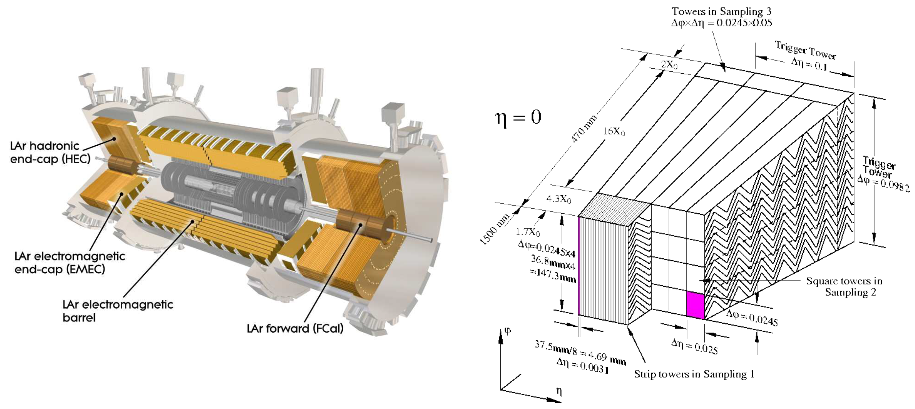
The ATLAS liquid argon (LAr) calorimeter [1,2] measures the energy and timing of photons, electrons, and hadrons that are produced by proton-proton collisions in the Large Hadron Collider (LHC). It is a sampling calorimeter with 182,468 cells in an accordion geometry of active (LAr) and absorber (lead) material, segmented into three longitudinal layers in the barrel with dedicated endcap detectors to cover the high range. Figure 1 shows a schematic view of the LAr calorimeter in the ATLAS detector, along with a diagram of the geometry and dimensions of a calorimeter slice.
The LAr calorimeter readout electronics system samples the cells at the LHC bunch crossing (BC) frequency of 40 MHz, and sends a digitized pulse off the detector for signal analysis and triggering. This readout system is separated into on- and off-detector components. The front-end board (FEB) is located directly on the cryostat that provides cooling for the LAr cells, in order to optimize the analog performance of the electronics. It is therefore subject to an environment with high radiation doses, a high magnetic field, and limited access during run periods, presenting a variety of challenges in the electronics design. Signals from the FEB are sent out of the ATLAS cavern to the off-detector electronics, which apply digital filtering to extract energy and time for each cell and pass salient information to the trigger and data acquisition systems.
The LHC is scheduled to undergo an upgrade beginning in 2029 to deliver a higher instantaneous luminosity up to 7.5 × 10 cm s, with approximately 200 simultaneous collisions expected in each BC. This leads to an increase in pileup, which refers to energy deposits from other simultaneous collisions or collisions in the adjacent bunch crossings. Two kinds of pileup can affect the measurement of LAr signals. In-time pileup comes from overlaid proton collisions within the same BC. Out-of-time pileup consists of energy that is leftover in the calorimeter from previous BCs, which accumulates because the LAr pulse signal takes approximately 25 BCs to read out.
The density of detector signals in this High Luminosity LHC (HL-LHC) will present new challenges for the subsystems, which will need to accommodate higher trigger rates and radiation doses. While the LAr cells will continue to perform within required specifications throughout the nearly ten year lifetime of the HL-LHC, the readout must be fully re-designed and replaced (the only exception is the cold pre-amplification and summing circuit system of the hadronic endcap, which will remain unchanged from its current state.) to continue delivering high-quality LAr data. This amounts to 1524 FEBs, 122 calibration boards, and all off-detector electronics. The new LAr readout will provide information from the entire calorimeter at full precision for more powerful trigger decisions. It has been organized into two stages: Phase-I, which has already been installed in the ATLAS cavern and is being commissioned for Run 3 of the LHC, and Phase-II, which is scheduled for installation in 2026 [3].
Design choices for the new LAr readout are motivated by key physics drivers of the HL-LHC physics program. Probing the TeV mass scale for new particles means that the calorimeter must be capable of providing precise measurements for very high energy electromagnetic decay byproducts. Further, the goal of better characterizing the Higgs boson requires excellent reconstructed mass resolution of the process. Specifically, the new readout must ensure that photons from are mostly digitized on High gain. This modifies the existing readout scheme where photons coming from a Higgs have a typical energy range at the value where the gain scale switches from Medium to High, thereby minimizing the gain inter-calibration systematic on the Higgs mass measurement. This leads to a readout design with only two gain scales (rather than the current three gain scales implemented in Run 2) [3].
The upgraded ATLAS trigger scheme must also be taken into consideration for the LAr readout design, as the off-detector electronics are responsible for providing LAr information to the trigger. The increase in trigger rate and latency for the HL-LHC motivates the adoption of a free-running all digital design for the LAr readout with no on-detector pipeline. The full data rate for the LAr calorimeter corresponds to approximately 350 Tbps. This new scheme allows for a sharper trigger turn-on to the efficiency plateau, while maintaining the ability to trigger on low momentum objects.
2. HL-LHC Readout Components
Figure 2 shows a block diagram of the full LAr calorimeter readout scheme for ATLAS in the HL-LHC. The physics goals of the experiment dictate specifications for the system. The readout must be able to handle a wide range of energies that may be deposited in a single cell during collisions, bounded by approximately 50 MeV at the lower end from electronic noise and reaching a maximum of approximately 3 TeV from electrons or photons produced in the decay of a new particle with mass (10) TeV. Therefore, the readout must have a high dynamic range, in this case 16-bits with 11-bit precision. This is implemented in two overlapping 14-bit gain scales. The electronic noise must be less than the typical energy deposited by a minimum ionizing particle passing through the LAr calorimeter. Stringent nonlinearity requirements are imposed to ensure accurate measurements, specifically <0.1% for cell energies up to approximately 300 GeV. Finally, as the electronics will not be replaced throughout the HL-LHC operating period, they must remain performant over the full expected radiation dose, corresponding to a total ionizing dose of 1400 Gy (safety factor 1.5), and a non-ionizing energy loss of <4.1 × 10 neutron equivalent per cm (safety factor 2).
2.1. Front End
The front end on-detector LAr electronics comprises the 2nd generation FEBs (FEB2) and the calibration boards. Each FEB2 and calibration board will have 128 data channels, and utilize the I2C configuration protocol. The unique requirements for the readout lead to the development of four full-custom application specific integrated circuits (ASICs) to be used on these boards. These are the preamplifier/shaper (PA/S), analog–digital converter (ADC), and calibration chips CLAROC and LADOC, each of which is described in detail below.
2.1.1. Preamplifier/Shaper
The PA/S chip is the first step in the readout chain after data leaves the LAr calorimeter cell. It performs analog processing on signals, namely amplification, splitting into two gain scales, and the application of a bipolar CR-(RC) shaping function to create the desired LAr pulse shape. This generates differential outputs that are passed to both the next element in the front-end readout chain, as well as to the L0 trigger.
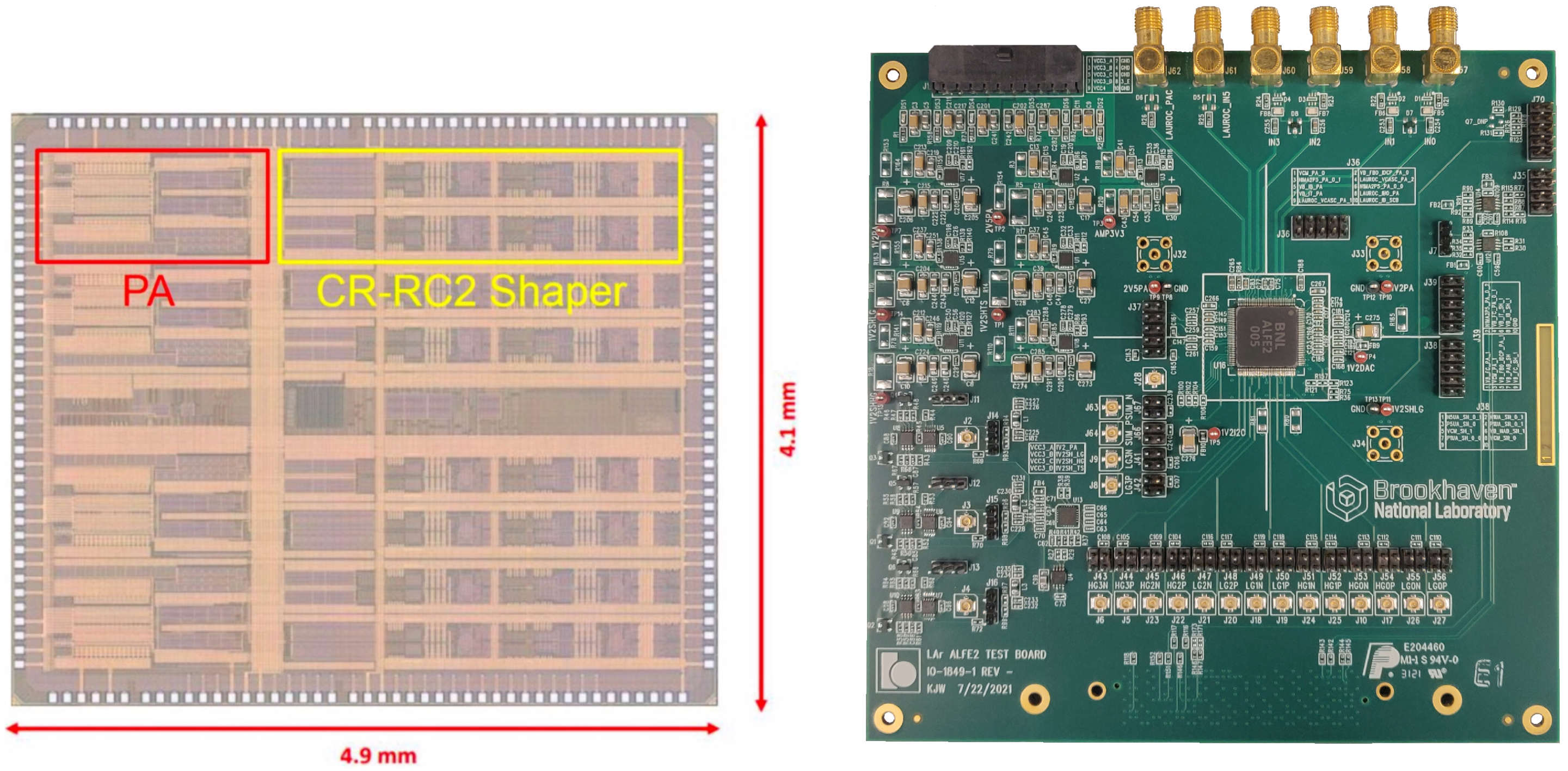
The candidate chosen for the PA/S on the FEB2 is the ALFE, which is the prototype custom ASIC built in 130 nm CMOS TSMC technology with 4 channels per ASIC. It has a tuneable input impedance to match the varying cell size across the calorimeter, as well as tuneable time constants for the shaping function, and can perform four channel summing for the hardware trigger. Figure 3 shows an image of the ALFE2 chip die, with specific circuit components highlighted, along with a picture of the testboard uses to make performance measurements. ALFE testing has resulted in an integral non-linearity <0.1%, as well as very low equivalent noise input of <150 nA and low crosstalk (<20 mV for the 50 input impedance configuration). Radiation testing also revealed that the ALFE maintains good performance after a 12 kGy dose, when only a 1.4 kGy dose is anticipated. As this prototype version of the PA/S chip is well within the necessary specifications, it will be re-packaged in a ball gate array (BGA) for the FEB2 prototype. Pre-production of ASICs can also begin, in preparation for an ultimate yield of approximately 80 thousand chips total (including spares).
2.1.2. Analog-Digital Converter
The PA/S passes differential signals to the ADC chip, which digitizes the incoming data at the LHC clock frequency of 40 MHz. The ASIC used for the HL-LHC is the eight channel COLUTA chip in 65 nm CMOS. The required 14-bit dynamic range is achieved by a 3-bit multiplying digital-analog converter (DAC) followed by 12-bit Successive Approximation Register (SAR), along with a Digital Data Processing Unit (DDPU) that applies calibration bit weights and serially transmits the digitized data. Figure 4 shows an image of the die for the prototype version, CV4, and the corresponding testboard for performance measurements.
CV4 delivers 1.2 ADC counts of noise on the pedestal, and an effective number of bits (ENOB) of 11.8 (11.5) for sine waves of 5 (8) MHz carrier frequencies. This exceeds the requirement of 11 ENOBs across the full dynamic range, and the CV4 also meets other specifications on nonlinearity and radiation tolerance. As with the ALFE, the CV4 will also be packaged in BGA for placement on the FEB2 prototype, and pre-production is scheduled to begin shortly.
2.1.3. FEB2 Pre-Prototype
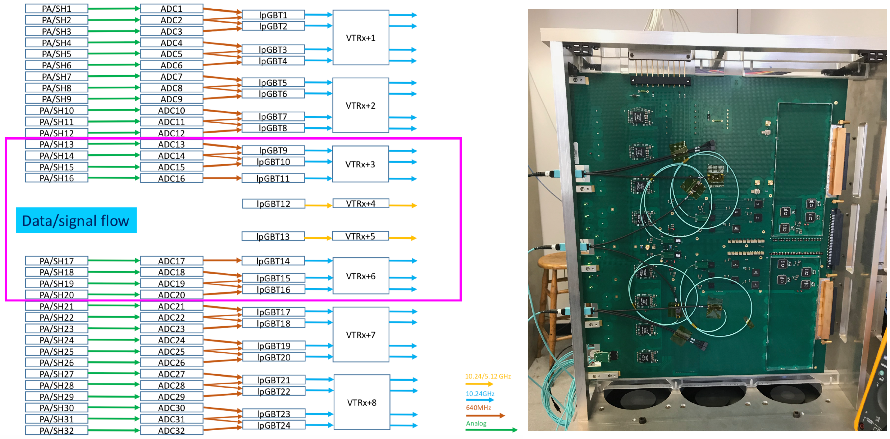
The integration of the FEB2 custom electronics into the full readout chain is tested with the pre-prototype of the FEB2. This so-called “slice" testboard has only 32 of 128 channels instrumented, enabling performance measurements of LAr pulses propagated through the full readout chain, as well as coherent noise and clock/configuration testing. Figure 5 shows a diagram of the data flow on the slice testboard, and an image of the board in its test setup. The slice testboard allowed for full validation of the slow control, monitoring, and redundancy of the bidirectional clock and control links, ensuring a robust configuration protocol and clock distribution.
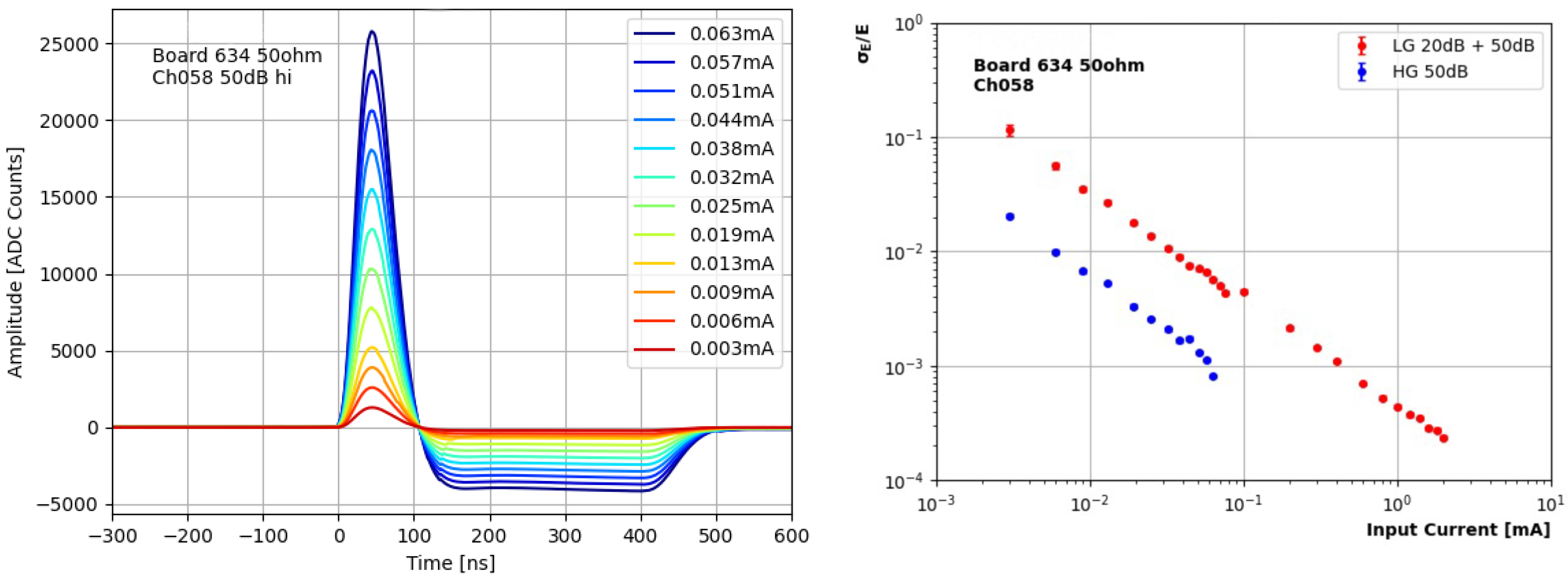
To assess the reconstruction capability of the slice testboard, energy and timing measurements of each LAr pulse are computed using optimal filtering coefficients (OFCs) [4]. These are computed using precision knowledge of the LAr pulse shape, allowing for robustness against distortion due to pileup. The OFCs are applied to samples from four points on the signal waveform, separated by 25 ns as dictated by the ADC frequency, and the energy and timing of the pulse can be calculated from linear combinations of the OFCs and sample values. Figure 6 shows pulses read out by the slice testboard at a variety of amplitudes, along with the obtained resolution on the energy measurement over the full dynamic range of the system. For the highest energy pulses, where the energy resolution is expected to be the best, the resolution defined as reaches approximately 0.02%, well below the specification of 0.25%. The timing resolution for these large pulses is approximately 50 ps, which is dominated by the clock jitter on the board. Multi-channel performance can also be studied, and the measured coherent noise was found to be less than a few percent of the total pulse size, with a low cross talk well below the percent level.
The next steps in FEB2 development include the design of the 128-channel prototype board, at which point tests can be performed with the proposed power distribution and on-detector crate. Production will consist of 1627 boards including spares.
2.1.4. Calibration System
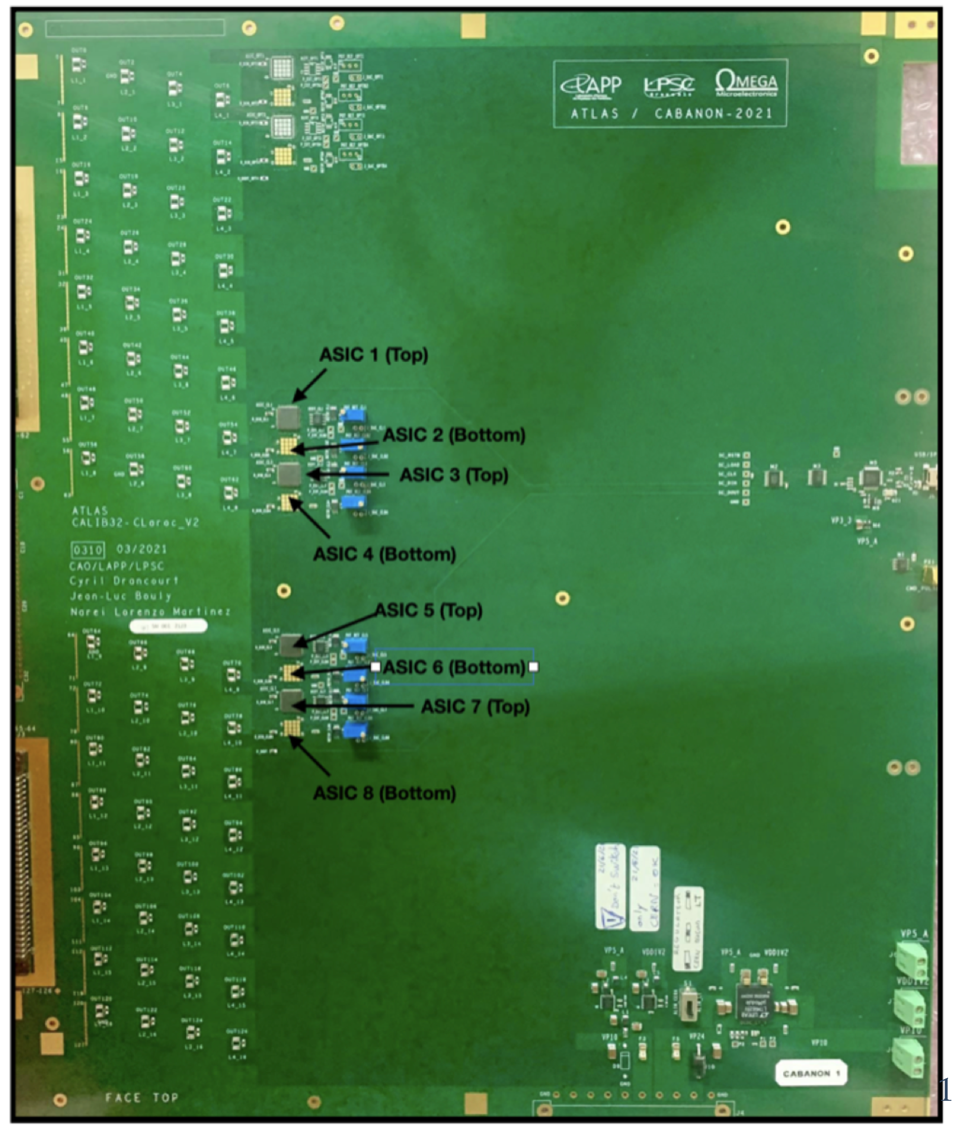
For maximal performance, the readout system must be calibrated with the injection of a precise calibration pulse. Key specifications for this system include an integral non-linearity <0.1% in the FEB2 high gain, <0.2% in the intermediate range (end of high gain up to 250 mA), and <1% in the high current range (250–300 mA), along with a uniformity <0.25%. The circuit that generates the calibration pulse contains two custom ASICs. The CLAROC creates the pulse by opening a high-frequency switch; as the requirements on pulse size mean that this chip needs a 7.5 V power source, this chip is designed in 180 nm XFAB technology. The LADOC is a custom 16-bit DAC that is used to command the switch with built-in 130 nm TSMC technology. The test setup with these ASICs indicates that they meet nearly all required specifications, with the exception of linearity and radiation hardness, which are anticipated to be resolved in prototype versions. A 32 channel pre-prototype board CABANON, analogous to the slice testboard, measured cross-talk <0.1% of the signal, in line with specifications, and allowed for a power distribution test comparing two different DC/DC convertor candidates. An image of this pre-prototype is given in Figure 7. Next generation versions of the CLAROC and LADOC have been designed to overcome non-linearity and radiation hardness issues, and are currently being fabricated. These chips will be packaged in BGA as with the FEB2 ASICs, and a 128-channel prototype design will be forthcoming, harmonizing the development of both front-end system boards.
2.2. Off Detector
The back-end electronics are located off the detector in the USA15 counting room, with no radiation from collisions. They consist of two systems: the LAr Timing System (LATS), and the LAr Signal Processor (LASP). The FEB2 boards connect to the off-detector electronics via optical links driven by lpGBT serializers.
2.2.1. Timing System
The LATS is responsible for the trigger, timing, and control (TTC) distribution to the front-end, configuration based on the lpGBT protocol, and monitoring of all 1524 FEB2 and 122 calibration boards, requiring a total of 3192 links. This is performed by the LATOURNETT board, which consists of 13 field programmable gate arrays (FPGAs). 12 of these are matrix FPGAs with both transmitters and receivers, each of which receives data from 1 FEB2, and the last FPGA has a centralized control role. The firmware for both of the FPGAs has been validated in simulation, and the power-up sequence has been verified with a dedicated testboard. Further testing will continue in parallel to the submission of a prototype board design, followed by integration tests with the on-detector electronics.
2.2.2. Signal Processor
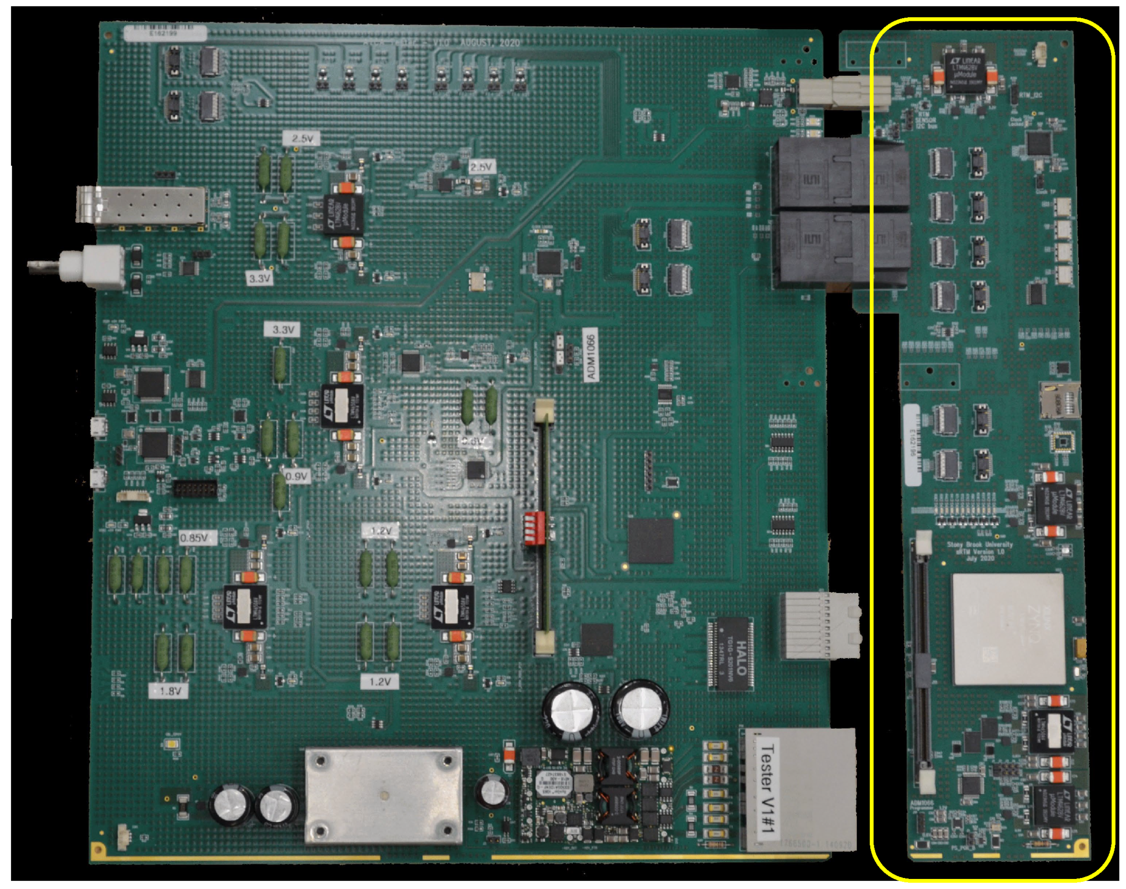
The LASP applies digital filtering to digitized waveforms received from FEB2, in order to calculate the energy and time of the pulse. It then transmits this high-level information to both the trigger and DAQ at 25 Gbps. This operation must be done online in two FPGAs on the LASP Main Blade combined with a Smart Rear Transition Module (SRTM). Between 200 and 300 of each board will be produced, with 6-8 FEB2 boards per blade.
A testboard has been produced with full capability, allowing for the validation of power sequencing, I2C configuration sensors, clock distribution, and FPGA configuration. A photograph of the test setup, with the LASP Main Blade and SRTM, is given in Figure 8. A complex firmware design has been produced that is highly modular, allowing for flexible integration of the number of FEB2 boards read by each FPGA. Measurements with these first testboards will inform the prototype design, particularly on the choice of FPGA, due to limitations on resource usage and a tight power budget.
3. Machine Learning Highlights on FPGAs
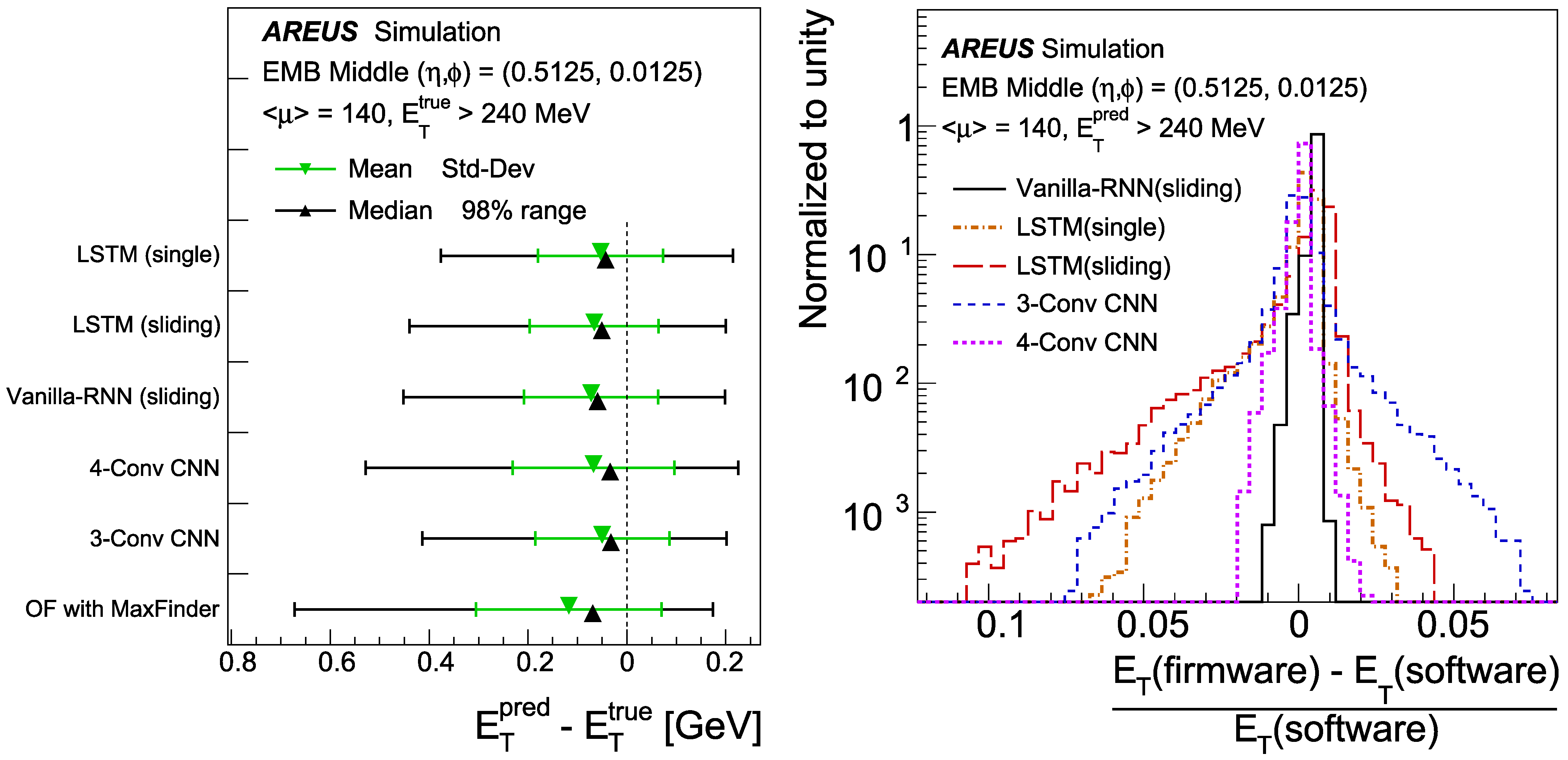
Signal processing on the LASP can benefit from machine learning (ML) techniques applied online at the FPGA level. Such advances are motivated by the increased pileup, which can degrade the energy and timing resolution as well as the performance of the trigger. Studies into the application of ML to mitigate pileup degradation utilize simulated digital pulses in a bunch train, which are used as input to three different architectures. The implementation described here achieves 37 neural nets (NNs) on one FPGA for a LASP running at 400 MHz, processing 10 channels each, with further optimizations ongoing [5].
The first architecture investigated is a convolution neural net (CNN), which has two separate phases for the tasks of pulse tagging and energy reconstruction. The first tagging layer is trained to detect energy deposits 3 above the electronic noise (240 MeV) using pulse samples for eight bunch crossings. The output of this tagging layer is a detection probability, which is passed along with the original sample sequence to the energy reconstruction layer, trained to reconstruct the amount of energy deposited in each cell. Parameters and architecture of the CNN are optimized based on high efficiency for detecting large energy deposits, high rejection of background signals, and good energy resolution.
Two sequence modeling architectures are also considered, a vanilla recurrent neural net (RNN) and long short-term memory (LSTM). These allow the modeling of data as a sequence of BCs, providing a better characterization particularly of out-of-time pileup. The LSTM demonstrates superior management of information through long sequences but its complexity means that strict limits on network size must be imposed for an FPGA implementation. The LSTM is used with both single BC inputs and a sliding window technique which incorporates up to four inputs from the current pulse and one from the previous pulse. The vanilla RNN can only be used with sliding window inputs as it does not have enough complexity to converge in a single cell.
Figure 9 shows a comparison of the performance of the various ML architectures, where the difference between the true and reconstructed transverse cell energy is compared for all methods. For reference, the analytical OFC method is included. All ML-based reconstructions outperform the legacy method in both accuracy and precision. Shown also is the performance comparison between NNs implemented via software-based calculations and via FPGA firmware, given as the relative difference in energy reconstruction between VHDL and Keras simulations. Very good agreement is observed between FPGA and software algorithms is observed, indicating that an NN-based reconstruction is capable of processing LAr signals in the HL-LHC readout and clearing the way for further development of these techniques in the LASP.
4. Conclusions
A status report is presented on the upgrade of the ATLAS LAr calorimeter for the HL-LHC era. The specifications of the upgrade are motivated by physics drivers for future LHC runs, leading to a free-running architecture that reads out the entire LAr calorimeter with full precision at the LHC clock of 40 MHz. Updates are given for all on- and off-detector components, namely the PA/S and ADC front-end ASICs, the pre-prototype FEB2 and calibration boards, the LATS, and the LASP. Comprehensive and performant results are presented utilizing pre-prototypes of key custom chips and boards. In the coming years, the final prototype design of all components must be designed, produced, and shown to continue meeting specifications in performance testing. Production and integration tests will also ramp up in preparation for the installation of all upgraded electronics into the ATLAS cavern starting in 2026.
Funding
The author is supported by the National Science Foundation under Grant No. PHY-2013070.
Data Availability Statement
Not applicable.
Conflicts of Interest
The authors declare no conflict of interest.
References
- ATLAS Collaboration. The ATLAS Experiment at the CERN Large Hadron Collider, JINST 3 S08003. 2008. Available online: https://iopscience.iop.org/article/10.1088/1748-0221/3/08/S08003/meta (accessed on 27 July 2022).
- ATLAS Collaboration. ATLAS Liquid Argon Calorimeter: Technical Design Report, CERN-LHCC-96-41. 1996. Available online: https://cds.cern.ch/record/331061 (accessed on 27 July 2022).
- ATLAS Collaboration. ATLAS Liquid Argon Calorimeter Phase-II Upgrade: Technical Design Report, CERN-LHCC-2017-018, ATLAS-TDR-027. 2017. Available online: https://cds.cern.ch/record/2285582 (accessed on 27 July 2022).
- Cleland, W.E.; Stern, E.G. Signal Processing Considerations for Liquid Ionization Calorimeters in a High Rate Environment. Nucl. Instrum. Methods Phys. Res. A Accel. Spectrom. Detect. Assoc. Equip. 1994, 338, 467–497. [Google Scholar] [CrossRef]
- Aad, G.; Berthold, A.-S.; Calvet, T.; Chiedde, N.; Fortin, E.M.; Fritzsche, N.; Hentges, R.; Laatu, L.A.O.; Monnier, E.; Straessner, A.; et al. Artificial Neural Networks on FPGAs for Real-Time Energy Reconstruction of the ATLAS LAr Calorimeters, ATL-LARG-PROC-2021-001. 2021. Available online: https://cds.cern.ch/record/2775033 (accessed on 27 July 2022).
Figure 1.
Schematic view of the different components of the ATLAS LAr calorimeter system (left), and a cut-out view of the calorimeter in the barrel including dimensions and coordinates (right) [1,2].

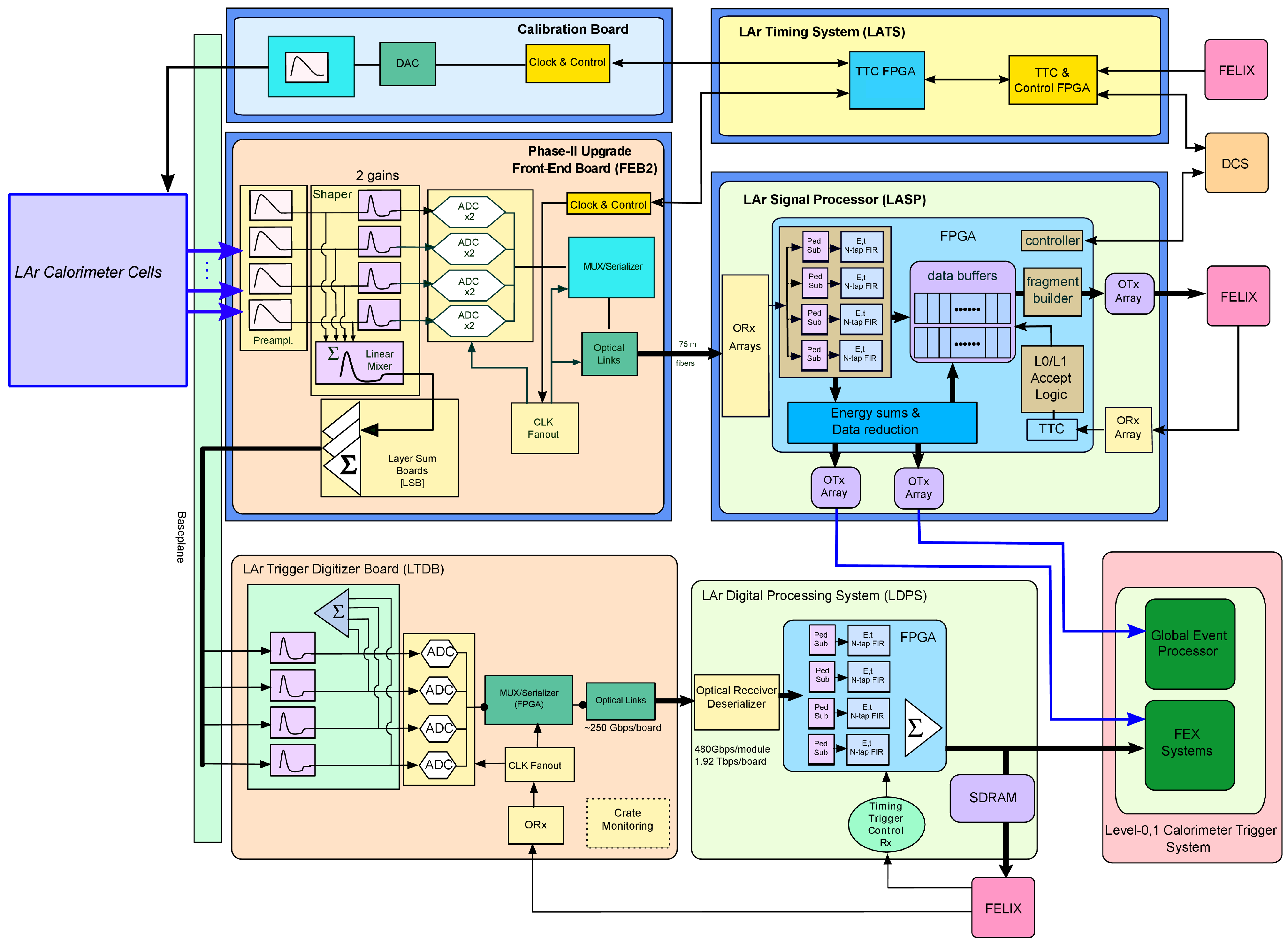
Figure 2.
Block diagram of the LAr readout in the HL-LHC, including all on- and off-detector electronics.
Figure 2.
Block diagram of the LAr readout in the HL-LHC, including all on- and off-detector electronics.

Figure 3.
Die image of the PA/S ALFE2 pre-prototype ASIC with key circuit elements outlined (left), and the corresponding ALFE2 testboard with soldered chip (right).
Figure 3.
Die image of the PA/S ALFE2 pre-prototype ASIC with key circuit elements outlined (left), and the corresponding ALFE2 testboard with soldered chip (right).

Figure 4.
Die image of the ADC CV4 pre-prototype ASIC with key circuit elements outlined (left), and the corresponding CV4 testboard with socketed chip (right).
Figure 4.
Die image of the ADC CV4 pre-prototype ASIC with key circuit elements outlined (left), and the corresponding CV4 testboard with socketed chip (right).

Figure 5.
Data flow diagram of LAr signals on the FEB2, with the 32 channel pre-prototype slice testboard highlighted in magenta (left), and an image of the slice testboard (right).
Figure 5.
Data flow diagram of LAr signals on the FEB2, with the 32 channel pre-prototype slice testboard highlighted in magenta (left), and an image of the slice testboard (right).

Figure 6.
Plot of reconstructed LAr pulses from the slice testboard across the full dynamic range (left), and the corresponding energy resolution as a function of input current (right).
Figure 6.
Plot of reconstructed LAr pulses from the slice testboard across the full dynamic range (left), and the corresponding energy resolution as a function of input current (right).

Figure 7.
Image of the CABANON pre-prototype test calibration board, with ASIC locations highlighted.
Figure 7.
Image of the CABANON pre-prototype test calibration board, with ASIC locations highlighted.

Figure 8.
Image of the LASP Main Blade and the STRM, with the SRTM outlined in yellow.

Figure 9.
Performance of ML signal processing methods implemented in FPGAs on the LASP, specifically the true vs. reconstruction transverse energy for all ML and the legacy methods (left), and the relative energy deviation of firmware ML implementations from the software results (right) [5].
Figure 9.
Performance of ML signal processing methods implemented in FPGAs on the LASP, specifically the true vs. reconstruction transverse energy for all ML and the legacy methods (left), and the relative energy deviation of firmware ML implementations from the software results (right) [5].

Publisher’s Note: MDPI stays neutral with regard to jurisdictional claims in published maps and institutional affiliations. |
© 2022 by the authors. Licensee MDPI, Basel, Switzerland. This article is an open access article distributed under the terms and conditions of the Creative Commons Attribution (CC BY) license (https://creativecommons.org/licenses/by/4.0/).
Share and Cite
MDPI and ACS Style
Gonski, J.; on behalf of the ATLAS Liquid Argon Calorimeter Group. Development of the ATLAS Liquid Argon Calorimeter Readout Electronics and Machine Learning for the HL-LHC. Instruments 2022, 6, 28. https://doi.org/10.3390/instruments6030028
AMA Style
Gonski J, on behalf of the ATLAS Liquid Argon Calorimeter Group. Development of the ATLAS Liquid Argon Calorimeter Readout Electronics and Machine Learning for the HL-LHC. Instruments. 2022; 6(3):28. https://doi.org/10.3390/instruments6030028
Chicago/Turabian StyleGonski, Julia, and on behalf of the ATLAS Liquid Argon Calorimeter Group. 2022. "Development of the ATLAS Liquid Argon Calorimeter Readout Electronics and Machine Learning for the HL-LHC" Instruments 6, no. 3: 28. https://doi.org/10.3390/instruments6030028