
Metastability Phenomena in VO2 Thin Films

 , ,
, , 
Abstract
:1. Introduction
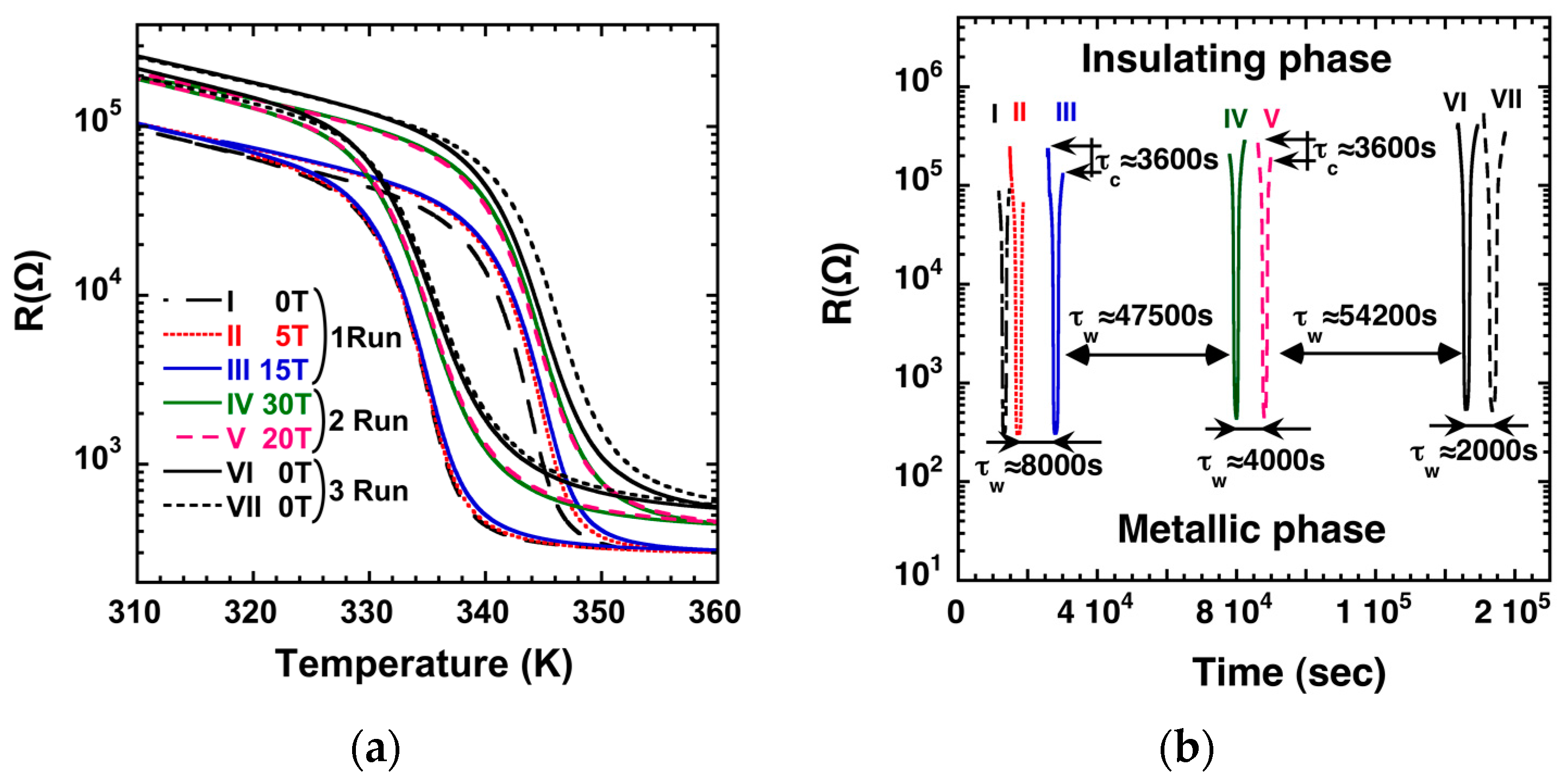
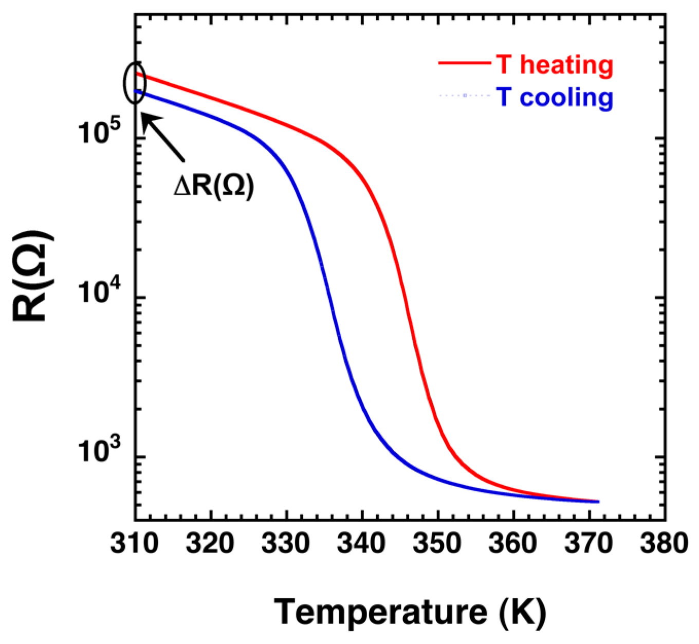
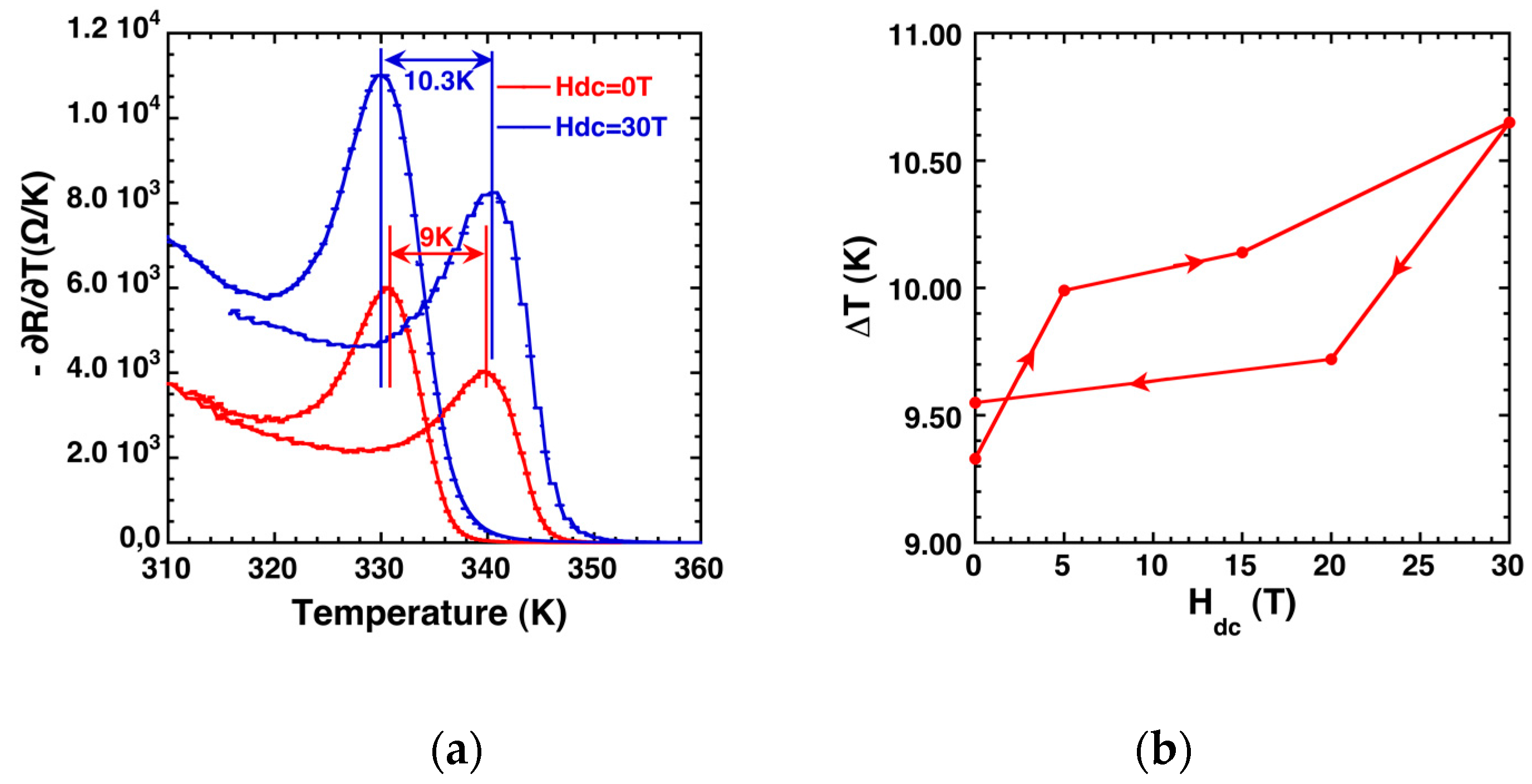
2. Results
3. Discussion
4. Materials and Methods
5. Conclusions
Acknowledgments
Author Contributions
Conflicts of Interest
References
- Pouget, J.; Launois, H.; Haenens, J.P.; Merenda, P.; Rice, T.M. Electron Localization Induced by Uniaxial Stress in Pure VO2. Phys. Rev. Lett. 1975, 35, 873–875. [Google Scholar] [CrossRef]
- Bianconi, A. Multiplet splitting of final-state configurations in x-ray-absorption spectrum of metal VO2: Effect of core-hole-screening, electron correlation, and metal-insulator transition. Phys. Rev. B 1982, 26, 2741–2747. [Google Scholar] [CrossRef]
- Aetukur, N.B.; Gray, A.X.; Drouard, M.; Cossale, M.; Gao, L.; Reid, A.H.; Kukreja, R.; Ohldag, H.; Jekins, C.A.; Arenholz, E.; et al. Control of the metal-insulator transition in vanadium dioxide by modifying orbital occupancy. Nat. Phys. 2013, 9, 661–666. [Google Scholar] [CrossRef]
- Cao, J.; Wu, J. Strain effect in low-dimensional transition metal oxides. Mater. Sci. Eng. 2011, R71, 35–52. [Google Scholar] [CrossRef]
- Nakano, N.; Shybaya, S.; Okuyama, D.; Hatano, T.; Ono, S.; Kawasaki, M.; Iwasa, Y.; Tokura, Y. Collective bulk carrier delocalization driven by electrostatic surface charge accumulation. Nature 2012, 487, 459–462. [Google Scholar] [CrossRef] [PubMed]
- Yoon, H.; Choi, M.; Lim, T.; Kwon, H.; Ihm, K.; Kim, J.K.; Choi, S.; Son, J. Reversible phase modulation and hydrogen storage in multivalent VO2 epitaxial thin films. Nat. Mater. 2016, 15, 1113–1119. [Google Scholar] [CrossRef] [PubMed]
- Cao, J.; Ertekin, E.; Srivasan, V.; Fan, W.; Huang, S.; Zheng, H.; Yim, J.W.L.; Khanal, D.R.; Ogletree, D.F.; Grosman, J.C.; et al. Strain engineering and one-dimensional organization of metal–insulator domains in single-crystal vanadium dioxide beams. Nat. Nanotechnol. 2009, 4, 732–737. [Google Scholar] [CrossRef] [PubMed]
- Poccia, N.; Ricci, A.; Campi, G.; Fratini, M.; Puri, A.; Di Gioacchino, D.; Marcelli, A.; Reynolds, M.; Burghammer, M.; Saini, N.L.; et al. Optimum inhomogeneity of local lattice distortions in La2CuO4 + y. Proc. Natl. Acad. Sci. USA 2012, 109, 15685. [Google Scholar] [CrossRef] [PubMed]
- Di Gioacchino, D.; Puri, A.; Marcelli, A.; Poccia, N.; Ricci, A.; Bianconi, A. The flux dynamics behavior of the two competing high temperature superconducting phases in underdoped LaCuO4.06. Phys. Chem. Chem. Phys. 2016, 18, 12534. [Google Scholar] [CrossRef] [PubMed]
- Ramírez, J.G.; Sharoni, A.; Dubi, Y.; Gómez, M.E.; Schuller, I.K. First-order reversal curve measurements of the metal-insulator transition in VO2: Signatures of persistent metallic domains. Phys. Rev. B 2009, 79, 235110. [Google Scholar] [CrossRef]
- Wei, J.; Wang, Z.; Chen, W.; Cobden, D.H. New aspects of the metal–insulator transition in single-domain vanadium dioxide nanobeams. Nat. Nanotechnol. 2009, 4, 420–424. [Google Scholar] [CrossRef] [PubMed]
- Berglund, C.N.; Guggenheim, H.J. Electronic Properties of VO2 near the Semiconductor-Metal Transition. Phys. Rev. 1969, 185, 1022–1033. [Google Scholar] [CrossRef]
- Agarwal, G.S.; Shenoy, S.R. Observability of hysteresis in first-order equilibrium and nonequilibrium phase transitions. Phys. Rev. A 1981, 23, 2719–2723. [Google Scholar] [CrossRef]
- Krusin-Elbaum, L.; Newns, D.M.; Zeng, H.; Derycke, V.; Sun, J.Z.; Sandstrom, R. Room-temperature ferromagnetic nanotubes controlled by electron or hole doping. Nature 2004, 431, 672–676. [Google Scholar] [CrossRef] [PubMed]
- Yan, T.H.; Nori, S.; Zhou, H.; Narayan, J. Defect-mediated room temperature ferromagnetism in vanadium dioxide thin films. Appl. Phys. Lett. 2009, 95, 102506. [Google Scholar]
- Bianconi, A.; Di Castro, D.; Bianconi, G.; Pifferi, A.; Saini, N.L.; Chou, F.C.; Johnston, D.C.; Colapietro, M. Coexistence of stripes and superconductivity: Tc amplification in a superlattice of superconducting stripes. Phys. C Supercond. 2000, 341–348, 1719–1722. [Google Scholar] [CrossRef]
- Di Castro, D.; Bianconi, G.; Colapietro, M.; Pifferi, A.; Saini, N.L.; Agrestini, S.; Bianconi, A. Evidence for the strain critical point in high Tc superconductors. Eur. Phys. J. B Condens. Matter Complex Syst. 2000, 18, 617–624. [Google Scholar] [CrossRef]
- Dagotto, E. Complexity in strongly correlated electronic system. Science 2005, 309, 257–262. [Google Scholar] [CrossRef] [PubMed]
- Campi, G.; Campi, G.; Bianconi, A.; Poccia, N.; Bianconi, G.; Barba, L.; Arrighetti, G.; Innocenti, D.; Karpinski, J.; Zhigadlo, N.D.; et al. Inhomogeneity of charge-density-wave order and quenched disorder in a high-Tc superconductor. Nature 2015, 525, 359–362. [Google Scholar] [CrossRef] [PubMed]
- Marcelli, A. Phase Separations in Highly Correlated Materials. Acta Phys. Polonica A 2016, 129, 264–269. [Google Scholar] [CrossRef]


© 2017 by the authors; licensee MDPI, Basel, Switzerland. This article is an open access article distributed under the terms and conditions of the Creative Commons Attribution (CC BY) license ( http://creativecommons.org/licenses/by/4.0/).
Share and Cite
Gioacchino, D.D.; Marcelli, A.; Puri, A.; Zou, C.; Fan, L.; Zeitler, U.; Bianconi, A. Metastability Phenomena in VO2 Thin Films. Condens. Matter 2017, 2, 10. https://doi.org/10.3390/condmat2010010
Gioacchino DD, Marcelli A, Puri A, Zou C, Fan L, Zeitler U, Bianconi A. Metastability Phenomena in VO2 Thin Films. Condensed Matter. 2017; 2(1):10. https://doi.org/10.3390/condmat2010010
Chicago/Turabian StyleGioacchino, Daniele Di, Augusto Marcelli, Alessandro Puri, Chongwen Zou, Lele Fan, Uli Zeitler, and Antonio Bianconi. 2017. "Metastability Phenomena in VO2 Thin Films" Condensed Matter 2, no. 1: 10. https://doi.org/10.3390/condmat2010010