
Sustainable Approach for the Development of TiO2-Based 3D Electrodes for Microsupercapacitors
by
 ,
,
Nathalie Poirot
1,
Marie Gabard
1,2,
Mohamed Boufnichel
3,
Rachelle Omnée
2,4 and
Encarnacion Raymundo-Piñero
2,4,* 1
GREMAN, UMR7347, CNRS/Université François Rabelais, IUT de Blois, 15 rue de la Chocolaterie, 41000 Blois, France
2
CNRS, CEMHTI UPR3079, Univ. Orléans, 1D Avenue de la Recherche Scientfique, 45071 Orleans, France
3
STMicroelectronics, 10 rue Thalès de Milet, 37071 Tours, France
4
Réseau sur le Stockage Electrochimique de l’Energie (RS2E), Cedex FR CNRS 3459, 80039 Amiens, France
*
Author to whom correspondence should be addressed.
Batteries 2023, 9(5), 258; https://doi.org/10.3390/batteries9050258
Submission received: 10 March 2023
/
Revised: 30 March 2023
/
Accepted: 14 April 2023
/
Published: 29 April 2023
(This article belongs to the Special Issue High-Performance and Sustainable Supercapacitors: Current Status and Perspective)
Abstract
:This study reports a sustainable approach for developing electrodes for microsupercapacitors. This approach includes the synthesis of TiO2 nanoparticles via a green sol–gel method and the deposition of thin films of that electrochemically active material on three-dimensional (3D) Si substrates with a high area enlargement factor (AEF) via a simple, fast, and inexpensive spin-coating pathway. The thickness of the film was first optimized via its deposition over two-dimensional (2D) substrates to achieve high capacitances to provide high energy density but also to deliver a good rate capability to ensure the power density required for a supercapacitor device. A film thickness of ~120 nm realizes the best compromise between the electronic/ionic conductivity and capacitance in a supercapacitor device. Such layers of TiO2 were successfully coated onto 3D microstructured substrates with different architectures, such as trenches and pillars, and different aspect ratios. The spin-coating-based route developed here has been established to be superior as, on the one hand, a conformal deposition can be achieved over high AEF subtracts, and on the other hand, the 3D electrodes present higher surface capacitances than those obtained using other deposition techniques. The rate capability and appreciable cyclability ensure a reliable supercapacitor behavior.
1. Introduction
The increasing need for miniaturized power sources and the diversification of microdevices has promoted interest in three-dimensional (3D) integrated energy storage components [1]. Structuring active materials on 3D supports affords electrochemical devices with advantages, such as a reduced device size and device fabrication cost and improved reliability and energy-related performances. Therefore, research in this area is extremely active, particularly in the fields of microbatteries, microsupercapacitors, fuel cells, solar cells, and metal–insulator–metal (MIM) capacitors [1,2,3,4,5,6,7,8,9,10,11,12,13,14,15,16,17,18,19,20,21,22,23,24,25]. In energy storage systems, such as batteries and supercapacitors, the integration of microsystems enables sustained and autonomous operation of electronic devices for applications such as wearable gadgets or wireless sensor networks.
However, decreasing the size of an energy storage device, such as a battery or a supercapacitor, requires researching strategies that do so without considerably decreasing its energy density. Because the energy density depends on the specific surface of the electrode–electrolyte interface, new advanced concepts have been proposed for nanostructuring electrodes using 3D templates/substrates such as nanowires (NWs), nanorods, nanosheets, or nanowalls [1,2,3,4,5,6,7,8,9,10]. For example, in the field of Li-ion microbatteries, Golodnitsky et al. [20] increased the capacity of a MoOySz thin film by 20–30 times by nanostructuring the electrode active material on a 3D glass microchannel plate (MCP) substrate and exhibited a reversible discharge capacity of 3.5 mAh cm−2.
The electrochemical performance of a nanostructured 3D electrode depends on the area enlargement factor (AEF), which represents the ratio between the 3D and two-dimensional (2D) surface areas (i.e., the gain obtained). To increase the energy performance substantially, the AEF must attain a high value. Nevertheless, one of the limitations to designing a high-AEF substrate is the fact that the geometrical structures of the 3D topology must be sufficiently spaced to allow the deposition of the electrode material thin film initially and subsequently access for the ions from the electrolyte to the electrode surface.
Among oxides such as MnO2 [15] and RuO2 [5], titanium dioxide, TiO2, is increasingly used as electrode material in energy storage microdevices, such as microbatteries and microsupercapacitors.
In addition to the well-known electrochemical properties of TiO2 as an electrode in energy storage systems, TiO2 has attracted interest primarily because, during the last few years, synthetic routes for thin films with controlled crystallite sizes and shapes and good adhesion to different supports have been reported. TiO2 thin films can be obtained via several methods [26] including sol–gel processes [27,28], spray pyrolysis [29], pulsed laser deposition [30,31], radio frequency magnetron sputtering (physical vapor deposition (PVD) method [32,33], and atomic layer deposition (ALD) [34]. Once the synthesis of TiO2 thin films was established, further structuration of TiO2 thin films on 3D supports was possible, opening the way for developing high-performance microdevices.
In the literature, several approaches have been reported for combining TiO2 thin films as active materials with different 3D substrates to form electrodes for microbatteries and microsupercapacitors. Cheah et al. [35] developed a 3D nano-architectured aluminum-based metallic current collector with an anatase TiO2 layer deposited via ALD as a negative electrode for a microbattery. For the same thickness of 17 nm of the TiO2 thin film, they reported a capacity of 1.1 µAh cm−2 for a planar Al plate substrate and a capacity of 11.2 µAh cm−2 for a 3D substrate based on Al nanorods with an AEF of 10. These results highlight the importance of the AEF, showing that the capacity values evolve linearly with the AEF value. The same conclusions were reported by Wang et al. [36], who used lengthy and small-diameter vertically grown Ni NWs synthesized using a porous anodic alumina template with a thin TiO2 layer deposited via ALD. For a thin layer of TiO2 with a thickness of 16 nm, the discharge capacity obtained was only 1.6 µAh cm−2 when using planar Ni foil as the support; however, the capacity increased up to 160 µAh cm−2 upon using Ni nanowires as the support with an AEF of ~65. Eustache et al. [17] reported that to optimize the surface capacity of TiO2-based microelectrodes; a balance must be reached between the AEF of the 3D topology and the thickness of the electroactive layer. In particular, Eustache et al. reported a novel 3D silicon microtube scaffold with an AEF of 30 having adequate space between and within microtubes to allow ALD of a Pt current collector and a TiO2 layer with a thickness as high as 150 nm. Such a configuration allows for reaching surface capacities as 200 µAh cm−2.
TiO2 has also been used as an electrode in microsupercapacitors because it exhibits capacitive behavior in aqueous electrolytes such as H2SO4 or Na2SO4 solutions. When using gel solutions of aqueous electrolytes, thin film electrodes comprising TiO2/carbon composites synthesized via a laser-related techniques for interdigitated planar devices exhibit capacitances from 9.9 mF cm−2 [37] to 27 mF cm−2 [38]. In the literature, two approaches have been reported for enlarging the electrode surface via 3D structuration: the use of TiO2 nanotube (NT) arrays [39] or TiO2 coating of Si NWs (SiNWs) [40,41]. Highly ordered TiO2 NT arrays with a diameter of ~170 nm and a length of 17.5 µm can be synthesized via anodization of a Ti foil. Further introducing oxygen vacancies in TiO2 increases the capacitance from 2 to 23 mF cm−2 [39], outperforming other TiO2 NTs in aqueous electrolytes [36,42,43,44,45,46,47]. TiO2-coated SiNWs with a length of 2–4 µm exhibit capacitances of ~3.5 mF cm−2. Nevertheless, all these materials have limited energy densities because the chosen aqueous electrolyte limits the operating voltage due to the electrochemical stability window of water. An organic solvent will be more advantageous in terms of electrochemical stability window allowing the system to operate up to higher voltages. In fact, the nanotexturation of TiO2 particles at the nanoscale affords the oxide in Li-based organic electrolytes with a pseudocapacitive character since the charge exchange can be almost continuous as a function of the potential [48,49]. This pseudocapacitive character affords fast charge–discharge kinetics, which is compatible with the power demand of a supercapacitor. To obtain a major contribution of capacitive processes and to keep a high rate capability, Sallaz et al. [50] reported that the thickness of a TiO2 film deposited on 2D Pt via ALD should not be more than 6–11 nm to find a balance between capacitance and rate capability. However, the effect of further structuration of TiO2 thin films on 3D substrates in the organic electrolyte–based microsupercapacitors has not been reported in the literature.
Therefore, this study aimed to use high–enlargement area supports deposited with TiO2 thin films as electrodes for microsupercapacitors with a Li-based organic electrolyte.
Among the various thin film deposition techniques, sol–gel synthesis followed by spin-coating was chosen because it is sustainable, simple, and inexpensive owing to the requirement of less equipment and energy compared to other processes as ALD, PVD, laser related, and so forth. Another advantage of this method is that it affords the flexibility to control the microstructure of the deposited film. Deposition of TiO2 thin films by spin-coating on porous structures remains a technical challenge and has seldom been reported in the literature. Zhang et al. [40] used spin-coating to coat SiNWs with TiO2 prepared via a sol–gel method—although the AEF of the substrate was not very high (SiNWs had a length of 2 µm), a nonhomogeneous TiO2 layer with island-like aggregates was obtained, indicating the difficulty of chemical deposition routes.
A unique strategy for using the spin-coating technique to prepare 3D nanotextured electrodes with a conformal active material layer was reported previously [51,52,53]. This strategy based on soft chemical routes for preparing 3D electrodes is followed in this study to prepare TiO2-based electrodes for being used in microsupercapacitors operating in an organic electrolyte. For increasing the surface area of the electrode, 3D Si structures comprising trenches or pillars are created using deep reactive ionic etching after the standard photolithography processes. Thereafter, conformal thin films coating the 3D substrates are obtained through the penetration of the TiO2 precursors inside the 3D structures and the uniform coverage of TiO2 over the walls. The electrochemical properties of anatase TiO2 pseudocapacitive thin films were optimized by controlling the microstructure and thickness of the active material film as well as by synthesizing Si substrates with a high AEF.
2. Materials and Methods
2.1. Preparation of 3D Substrate Materials
3D Si substrate preparation was performed according to the literature [51]. In brief, the silicon substrate was a 150 mm diameter, p-type (100) silicon wafer (Sil’tronix, Archamps, France) with a thickness of 600–650 µm and an electrical resistivity of 0.001–0.002 Ω cm. To synthesize high-aspect-ratio (AR) structures on Si substrates, the Bosch process was used. The Bosch process, preferred for industrial applications, comprises alternating isotropic etching (SF6 plasma) and deposition steps (C4F6 plasma) at an ambient temperature [54]. Trench or pillar structures with an AR of 9 and 29 were obtained, respectively. The Si substrates were cleaned after the Bosch process to remove chemical residues by washing with a 40 wt% hydrofluoric acid (HF) solution, followed by the Radio Corporation of America (RCA) method [55]. In the RCA method, the Si substrates were immersed in a 5:1:1 mixture of H2O, H2O2, and NH4OH and heated at ~75–80 °C for 10 min.
2.2. Synthesis and Deposition of TiO2 Layers on 2D and 3D Substrates
For TiO2 preparation, a simple and scalable sol–gel method reported in the literature was used [26]. Briefly, 2.86 mL of tetrabutyl titanate (Acros Organics, Fisher Scientific SAS, Illkirch, France), 0.86 mL of acetylacetone (Merck KGaA, Darmstadt, Germany, 99% purity), and 1.14 mL of water were mixed. Propanol (Honeywell, Charlotte, North Carolina, US, purity ≥ 99.8%) was added to the mixture to obtain 20 mL of sol and to achieve a Ti concentration of 0.42 mol L−1 (sol S1). Two other mixed sols with different Ti concentrations were prepared as described above (sol S2 with a Ti concentration of 0.21 mol L−1 and sol S3 with a Ti concentration of 0.105 mol L−1). These sols were magnetically stirred for a few minutes. The sols were deposited on the 2D or 3D Si substrate via spin-coating using a particular method we developed for other materials [51,52,53]. The procedure includes adding a polyester resin (PE-NORSODYNE S 2010 V) to the S1, S2 or S3 solutions in a 4:1 mass ratio. The resin/sol mixtures were deposited on a 2 cm × 2 cm 2D or 3D silicon substrate using a spin coater (SPS-Europe Spin150) with a ramp rate of 2000 rpm/s and a spin speed of 3000 rpm for 30 s. This resin/sol mixture deposition was followed by thermal treatment on hot plates to remove the resin and solvents (175 °C for 5 min and 375 °C for 10 min) and rapid thermic annealing at 700 °C to crystalize the oxide layer.
The above procedure using sols S1, S2, and S3, allows the formation of TiO2 thin films with a thickness of 50 nm, 40 nm, and 20 nm, respectively. A layer with a thickness of 90 nm was formed by coating sol S1 and after sol S2. For a TiO2 layer thickness of 120 nm, 200 nm, and 300 nm, the process has been repeated two, four and five times, respectively, using sol S1.
To ensure good electrical contact between the electrode and the current collector during electrochemical characterizations, a 200 nm-thick Ti layer was deposited by PVD (Plassys MP650s) on the backside of the samples (sputtering rate = 1.7 nm/s, time = ~120 s).
2.3. Physico-Chemical and Electrochemical Characterization
Scanning electron microscopy (SEM) was performed on cross-sectional samples using Zeiss Ultra plus and Mira3 TESCAN microscopes with a very low accelerating voltage (4–5 kV).
The presence of the anatase phase and its phase purity in the TiO2 thin films were confirmed by X-ray diffraction (XRD) [Bruker D8 advance diffractometer with CuKα radiations; λ = 1.5418 Å]. XRD patterns were collected with a step size of 0.02° in an angular range from 20° to 60° at room temperature.
For electrochemical measurements, half-cells were prepared in an argon-filled glove box using Swagelok-type cells. The working electrode was dried Si/TiO2 materials, and the counter and reference electrodes were lithium foil. The working electrodes had a rectangular shape with a 0.49 cm2 surface. The working electrode and the Li foil were separated with two glass microfiber membranes (Whatman GF/C, FisherbrandTM, Fisher Scientific SAS, Illkirch, France) impregnated with 1 mol L−1 lithium hexafluorophosphate (LiPF6) dissolved in a 1:1:3 mixture of ethylene carbonate (EC, Sigma Aldrich®, Merck KGaA, Darmstadt, Germany, 99% purity), propylene carbonate (PC, Sigma Aldrich®, 99.7% purity), and dimethyl carbonate (DMC, Sigma Aldrich®, >99% purity) by mass. Electrochemical measurements were made performed using a VMP3 multichannel potentiostat (Biologic, Seyssinet-Pariset, France). Cyclic voltammetry (CVs) was performed at a scan rate of 1 mV s−1 between 1.0 and 3.0 V versus Li/Li+ for TiO2 electrodes. Galvanostatic charge–discharge cycling was performed at different current densities with potential limits cut-off between 1.0 V and 3.0 V versus Li/Li+ at charges densities from 0.02 to 0.5 mA cm−2. Impedance spectroscopy measurements were performed by applying an ac signal of 20 mV in the range from 10 kHz to 1 mHz. Surface capacitance values were obtained from galvanostatic charge–discharge cycling using the following equations:
where I is the current (amperes), ∆t is the discharging time (seconds), ∆V is the potential window after removing the ohmic drop (volts), and S is the geometrical surface of the sample (cm−2). Average values from three to five cells are presented.
3. Results and Discussion
3.1. 2D Electrodes
TiO2 layers were first deposited on 2D structured Si wafers to validate the deposition process and determine the optimal thickness of the active material layer in the electrode for optimal electrochemical performance.
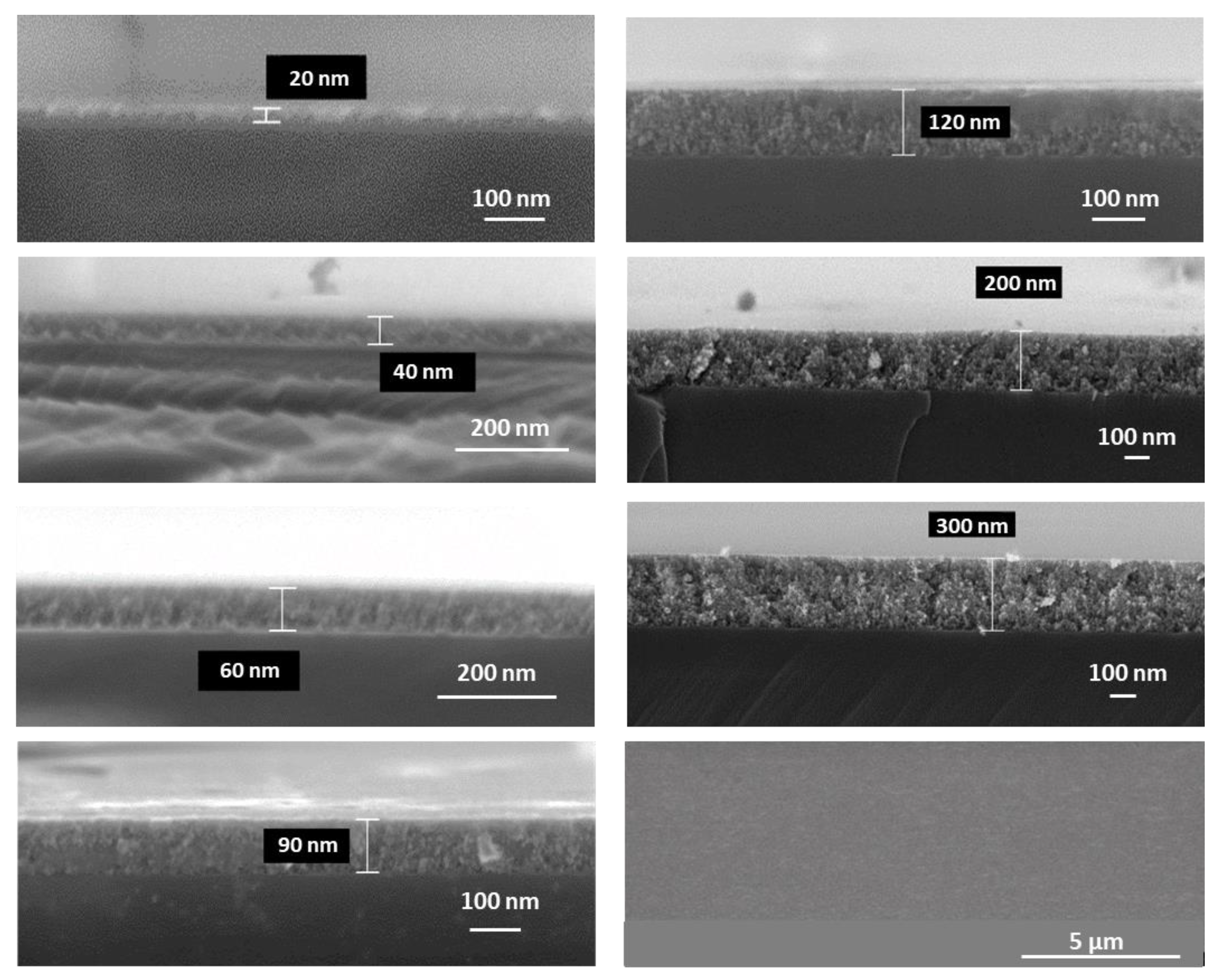
Figure 1 shows the SEM images of the 2D electrodes obtained after the deposition of TiO2 layers of different thicknesses on the Si substrate.
Figure 1 shows how the deposition of the sol in the presence of a PE resin, followed by the calcination step, affords homogeneous TiO2 films without cracks and fissures. The films comprise small and interconnected oxide nanoparticles and exhibit good adhesion to the Si substrate. The SEM images of the 2D electrodes confirm that the thickness of the TiO2 film can be precisely controlled between 20 and 60 nm by varying the sol concentration or layer-by-layer coating to obtain thicker films. The SEM images for the 120 to 300 nm films reveal any dead space between the deposited layers. Even if TiO2 layers with a thickness of 120 nm, 200 nm, and 300 nm are obtained by depositing sol S1 two, four, and five times, respectively, a continuous and homogeneous oxide layer without any interface is observed. Therefore, Figure 1 confirms the efficiency of depositing a TiO2 sol by spin-coating for obtaining homogeneous TiO2 layers without cracks and fissures (see the top view in Figure 1) of a desired thickness on a Si substrate.
To determine if the presence of PE resin during the sol deposition process affects the structure and crystallinity of TiO2, XRD of TiO2 films was performed, and the spectra of TiO2 films were compared to those of a TiO2 powder obtained using the same synthesis procedure in the absence of PE resin. Figure 2 shows that the XRD pattern of the TiO2 powder obtained via the sol–gel method is consistent with the anatase crystalline phase (reference PDF 01-013-1764) [56]. The XRD pattern of a 300 nm-thick TiO2 film deposited on a Si supports the XRD presents, in addition to the reflections of Si metal (XRD pattern of the Si support included in Figure 2), a visible anatase phase ((101) peak). Therefore, the deposition method does not impact the structure or crystallinity of TiO2, and the desired anatase phase was obtained for the TiO2 thin films.
3.2. Electrochemical Characterization of 2D Electrodes
Figure 3 shows the CV profiles (Figure 3a) and the galvanostatic charge–discharge (Figure 3b) curves for TiO2 films of different thicknesses deposited on a planar substrate obtained in a half-cell using an organic electrolyte (1 mol·L−1 LiPF6 in 1:1:3 EC:PC:DMC).
The CVs shown in Figure 3a present the typical signature of a nanosized TiO2 film in organic electrolytes exhibiting a capacitive contribution and Ti4+/Ti3+ redox peaks, which may originate from multiple lithium sites in the TiO2 structure [57]. The galvanostatic charge–discharge profiles presented in Figure 3b at a moderately high charge density of 0.1 mA cm−1 show a typical capacitive behavior, confirming the pseudocapacitive character of the nanosized TiO2 comprising the thin films where diffusion-controlled lithium-ion intercalation processes are replaced by surface reactions [48,49].
The effect of the thickness of TiO2 film on the electrochemical performance of the 2D electrodes was studied. Figure 3 exhibits that the capacitance of TiO2 increases when the thickness of the film increases from 20 to 90 nm, as shown by an increase in the area of the CV (Figure 3a). This increase in capacitance can be associated with an increase in TiO2 content taking part in the surface lithiation/delithiation process. However, the capacitance stabilizes for thickness going up to 120 nm for a strong decrease when the thickness of the film is increased up to 200 nm. The same observations can be made from the galvanostatic charge–discharge profiles shown in Figure 3b, where the discharge time increases for films with a thickness of 20–120 nm and then decrease for films with a thickness of 200 nm. Therefore, there are some limitations in charge diffusion when the film thickness is increased. To assess the optimal thickness of the TiO2 film, it is necessary to find a good compromise between surface capacitance and rate capability, and it is essential to evaluate their electrochemical performance at different charge densities.
Figure 4a shows the surface capacitance as a function of TiO2 thickness, obtained from galvanostatic charge–discharge experiments by applying current densities from 0.01 mA cm−2 to 0.2 mA cm−2.
Figure 4a shows the same tendency of the surface capacitance versus the TiO2 film thickness discussed above for 0.1 mA cm−2 (Figure 3b) for all the current densities. We observed an increase in the surface capacitance when the thickness of the film increased from 20 to 120 nm, followed by a noticeable decrease in the surface capacitance for the film with a thickness of 200 nm at low current densities, where faradic reactions have an important contribution toward the capacitance, or at high current densities, where the main processes are capacitive. These results indicate that the decrease in surface capacitance of the TiO2 when the thin films have a thickness of 200 nm is due to limitations from electronic and ionic conductions. That affirmation was confirmed using impedance spectroscopy over cells having electrodes with different thicknesses. Figure 4b shows the Nyquist plots obtained using electrodes with 120 nm and 200 nm-thick TiO2 layers. In the Nyquist plot of the electrode with a 200 nm-thick TiO2 layer, the electrical series resistance obtained at high frequencies related to the electronic resistance of materials and interfaces, and the electric distributed resistance obtained at lower frequencies related to the diffusion of ions at the electrode–electrolyte interface, increase. These results indicate that for a 200 nm-thick layer of the active material, the electrons have difficulty reaching the interface owing to the low electrical conductivity of TiO2, which also hinders the diffusion of lithium ions. Therefore, 120 nm is the optimal film thickness that realizes a suitable compromise that leads to good capacitance while imposing limited constraints on the electric/ionic conductivity. The capacitance values of ~8.1 mF cm−2 at 0.01 mA cm−2 (corresponding to ~4.5 µAh cm−2) for the 120 nm-thick film are similar to the values reported in the literature for 2D electrodes operating in organic electrolytes with TiO2 films prepared using ALD, making a substantial contribution to the development of capacitive processes to be used in supercapacitors [50].
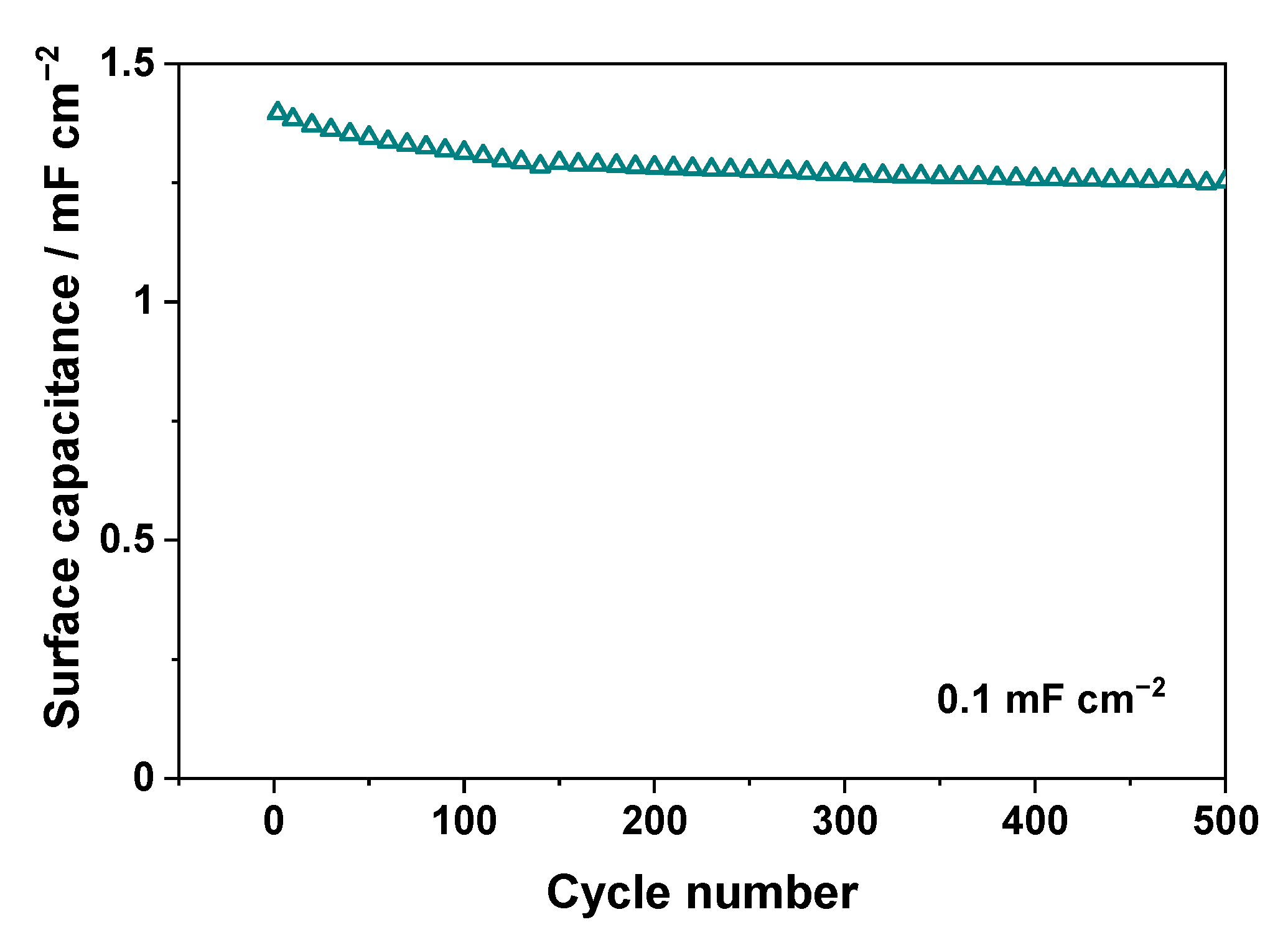
Finally, an aging test was conducted to assess the integrity of the film and the quality of the substrate/active material interface. For instance, Figure 5 shows the evolution of the surface capacity for a 120 nm-thick TiO2 layer coated onto a Si planar substrate via the galvanostatic charge–discharge cycles performed at a current density of 0.1 mA cm−2. After an initial decrease in the values of the surface capacitance, the system is stabilized, and the quality of the deposited film and the Si/TiO2 interface is established.
In conclusion, the results show that the proposed method presented is efficient at depositing homogeneous thin films of TiO2 exhibiting good adhesion to the Si substrate for use as electrodes in supercapacitors. From the above results, a TiO2 layer having a thickness of 120 nm is selected to be deposited over 3D supports having high surface areas for optimal performance.
3.3. 3D Electrodes
3.3.1. 3D Substrates
Figure 6 shows SEM images of the 3D supports with different topologies and ARs. The topologies used were trenches with ARs of 29 and 9 (Figure 6a,b) and pillars with an AR of 29 (Figure 6c).
The dimensions of the 3D structures are given in Table 1. The depth and width of the structures were estimated using SEM after etching.
The increase of the surface area enlargement depends on the width and depth of trenches or pillars and the spacing between these structures.
Taking into account a straight 3D template of a trench topology, as presented in Figure 6d, the surface AEF for trenches can be calculated according to the following equation [58]:
where S2D and S3D stand for the surface area of the 2D and 3D topology having the same footprint area, L is the overall length of the sample, w is the trenches width, and s is the spacing between trenches, as shown in Figure 6d.
For pillars, the surface AEF can be calculated according to the following equation [17]:
where w and d are the pillar diameter and the etched depth, respectively, and h and v are the horizontal pitch and vertical pitch, respectively, as shown in Figure 6d. The AR is the ratio of the pillar depth to the pillar width.
Figure 6 shows that the trenches with an AR of 29 are deeper (117 µm) than those with a lower AR of 9 (52 µm). Therefore, based on Equation (1), for trenches with ARs of 9 and 29, a footprint area of 1 cm2 is developed into 12.6 and 34.4 cm2 of useful surface area, respectively (Table 1). For pillars with an AR of 29, the depth is 144 µm, being higher than that for trenches with the same AR. Using Equation (2), for those pillars with an AR of 29, a footprint area of 1 cm2 is developed into 32.4 cm2 of useful surface area. The AEF uncertainty values are 3% after introducing the experimental values of the different parameters used in Equations (1) and (2).
3.3.2. TiO2 Coating on 3D Substrates
The same sustainable liquid route used for depositing homogeneous TiO2 layers on 2D Si supports was used for coating the 3D supports. This particular route was developed as an alternative to techniques used for coating 3D structures, such as ALD or PLD [56,57,58]. Indeed, when depositing films on high-AR 3D structures, conventional liquid routes become inefficient: the capillary force proportionally increases with the AR, where AR = etching depth ÷ trench or pillar width. Therefore, the challenge is to achieve a conformal deposition of an electrochemically active thin film on a 3D substrate having a high AEF via the liquid route.
The capillary process follows the Jurin law and can be expressed by Equation (3):
where h is the height of the liquid, γ is the surface tension of the liquid, θ is the contact angle of the liquid on the substrate, ρ is the solution density, r is the tube radius, and g is the gravitational acceleration. The contact angle and good wettability with Si substrates can be controlled by changing the solvent and/or adding additives. However, to obtain a good TiO2 coating on 3D substrates with aspect ratios as high as 29, the viscosity of the precursor solution is the key parameter. Herein, a polyester resin was added to the solution containing TiO2 precursors, that is, an 80% polyester and 20% precursor solution [52]. The addition of polyester increases the viscosity of the TiO2 precursors solution (85 mPa s), which increases the adhesion of the mixture to the substrate during deposition via simple spin-coating.
The cross-sectional views after solution deposition and the following thermal treatments confirm that the solution penetrated inside the 3D structures, and a TiO2 layer uniformly covering the walls was created (Figure 7). The general view of the three different electrodes shows that even for the subtracts with an AEF of 29, the TiO2 layer is homogeneous and does not form large agglomerates, as has been observed for low AEF subtracts prepared without the addition of a resin for adjusting the sol density [40]. Moreover, using this method, no cracks or fissures are observed (Figure 7f,i) as for the 2D supports (Figure 1), which is contrary to what has been predicted by Seemann et al. [59].
Different locations (top, middle, and bottom) inside the trenches and micropillars were inspected at high magnifications to determine the thickness of the TiO2 films after performing a minimum average of 12 observations. Under such magnifications, it can be observed that the proposed coating method allows the active materials to penetrate inside the 3D structures and cover the walls from the top to the bottom of the substrate homogeneously. The thickness of the TiO2 layers is ~110 nm for the trenches with AEF values of 9 and 29 (Figure 7a–c or Figure 7d–f, respectively) and ~130 nm for the pillars with an AEF of 29 (Figure 7g–i). Therefore, the values are in the range of the optimal thickness determined when exploring the electrochemical performance with respect to 2D substrates. The SEM images also reveal that the different 3D-coated architectures have sufficient space between the trenches and pillars to facilitate the diffusion of the liquid electrolyte during electrochemical measurements.
3.3.3. Electrochemical Performance of 3D Electrodes
Figure 8a shows the CV profiles of electrodes having a TiO2 layer of the same thickness but with a 2D or 3D support with an AR of 29. The CV profiles for 3D electrodes exhibit the same shape as those for 2D electrodes having a capacitive and Faradic contribution with the different reduction and oxidation waves appearing at the same potentials (compare with Figure 3 for more details in 2D electrodes). Therefore the structuration of the Si substrate does not have any influence on the chemical nature or structure of TiO2 prepared via the sol–gel route. However, increasing the AR of the Si support from 1 to 29 considerably affects the area inside the CV profile. Increasing the specific surface area of the electrode up to 34.4 cm2 leads to a substantial increase in its surface capacitance.
This effect was well established when the surface capacitance and rate capabilities of the 3D electrodes were quantified based on the galvanostatic charge–discharge cycles at current densities ranging from 0.01 to 0.5 mA cm−2 (Figure 8b and Table 2).
Figure 8b shows that for a low current density, i.e., 0.05 mA cm−2, the surface discharge capacitance follows the trend of the AEF. The surface capacity is multiplied by factors of 9.5 and 25.2 when switching from 2D to 3D electrodes, with trench topologies having AEFs of 12.6 and 34.4, respectively. For the 3D electrodes having the pillar topology, the capacitance enhancement at low current densities is less than expected because it is multiplied by a factor of 16.0 even when the AEF is 32.4. Regarding the rate capability, Figure 8b shows that the topology in trenches is more efficient than that in pillars. The electrode with the pillars topology does not operate at current densities >0.3 mA cm−2, while the electrode with the trench topology, having the same aspect ratio of 29, is able to retain a surface capacitance of 28.8 mF cm−2 as the charge density increases 10-fold from 0.05 to 0.5 mA cm−2. Therefore, the topology in the trenches allows a simultaneous improvement in the energy density, as the surface capacitance increases, and the power density, thereby addressing the requirements of a supercapacitor. The differences observed between the topologies could be owing to the quality of the TiO2/Si interface. Depositing a layer of TiO2 nanoparticles over the straight surface of the trenches can lead to superior adhesion compared to deposition over the curved surfaces of the pillars. Such interfacial issues have a substantial impact on the electrochemical performance when operating with low-conductive active materials, such as TiO2.
Figure 9 exhibits the advantages of using the 3D trench topology for supercapacitor applications. In Figure 9, the experimental and theoretical surface capacitances obtained at different charge densities are plotted against the surface AEF.
For the very low current density of 0.01 mA cm−2 (Figure 9a,b), the surface capacitance does not increase with the enlargement of the surface as expected. The surface capacitance value increases from 8.1 mF cm−2 to 85.0 mF cm−2 when the surface area increases from 1 cm2 to 34.4 cm2 instead of reaching the theoretical value of 278.6 mF cm−2. These results indicate that the diffusion-controlled processes arising in the bulk of the particles on the application of low current densities are favored in a 2D topology. When the current density increases, the measured surface capacitance approaches the theoretical capacitance and a perfect correlation between the values is obtained for current densities of 0.1–0.2 mA cm−2 (Figure 9c,d). For illustration, at 0.1 mA cm−2, the experimental and theoretical surface capacitance values for a 3D electrode with a surface area of 34.4 cm2 are 51.9 and 54.3 mF cm−2, respectively. These results are in line with the fact that the contribution of surface capacitive processes increases with current density. Figure 9e,f shows that these surface capacitive processes are favored in a 3D trench topology for high current densities. For current densities >0.2 mA cm−2, the experimental surface capacitance values obtained for the high surface area 3D electrodes are higher than the theoretical ones calculated from the capacitances obtained with the 2D electrodes. Therefore, trenches are the ideal topology for developing high-energy and high-power microsupercapacitors.
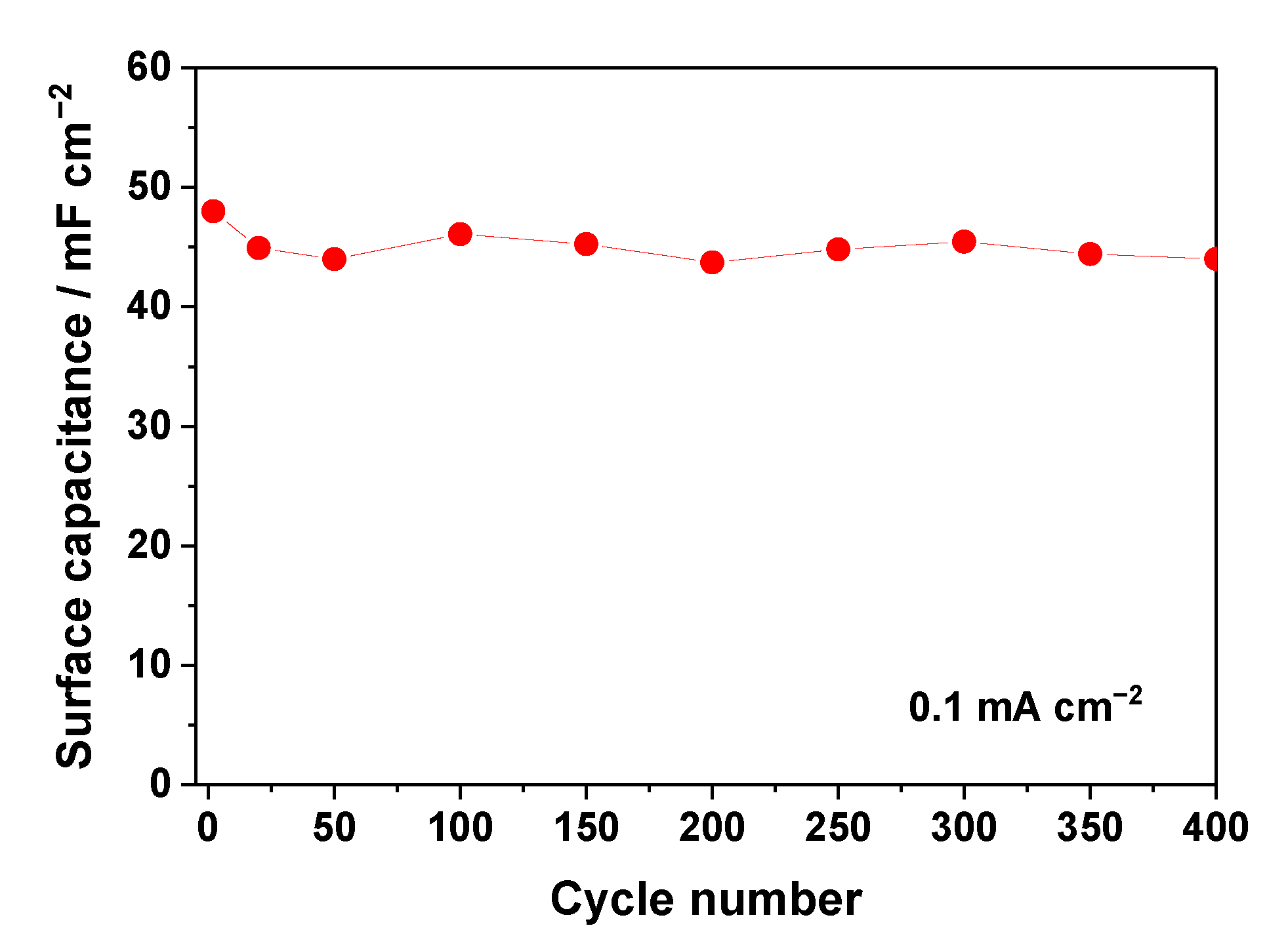
Moreover, the quality of the TiO2 adhesion layer over this high-AR 3D support with trench topology is demonstrated by a remarkable cycle life. Figure 10 shows the change in surface capacitance with galvanostatic charge–discharge cycles at a current density of 0.1 mA cm−2. After an increase in capacitance during the initial cycles, a stable capacitance is recorded for more than 400 cycles with an average surface-specific capacitance of 45.0 mF cm−2.
The particular topology of the electrode with trenches having a high surface area and a homogeneous layer of 120 nm of TiO2 allows electrochemical performances to outperform the ones shown in the literature. For comparison, TiO2 heterogeneously deposited via a classical chemical route or spin-coating over 2 µm depth SiNWs exhibited a capacitance of 3.55 mF cm−2 at 0.1 mA cm−2 [40], whereas a capacitance of 51.9 mF cm−2 was recorded in this study at the same current density.
Moreover, the surface capacitance achieved at a low current density for the TiO2 over the trenches, i.e., 85.0 mF cm−2 at 0.01 mA cm−2, is superior to those achieved for an ALD-deposited H-doped TiO2 layer of 20-nm thickness over SiNWs, i.e., 3.36 mF cm−2 at 0.035 mA cm−2 [41] and even to the high capacitance values O-doped TiO2 nanotube arrays with a surface capacitance of 23.24 mF cm−2 reported in a previous study [39]. Moreover, the specific capacitance values extracted from the literature and discussed above have been achieved using Na2SO4-based aqueous electrolytes, while a LiPF6-based organic electrolyte has been used herein. Operating in organic electrolytes affords the possibility of increasing the operating voltage and energy stored in comparison to systems using aqueous ones.
4. Conclusions
A sustainable approach to depositing TiO2 layers onto 3D Si substrates with different aspect ratios using a liquid route and spin coating has been developed herein. This method was selected because it is relatively simple, rapid, and inexpensive. Moreover, it could be used in industrial applications. The proposed method is effective in achieving a homogenous TiO2 thin film coating on 3D substrates with aspect ratios as high as 29 because the precursor solution with a modulated viscosity penetrates inside the 3D structures and uniformly covers the walls. The thickness of the active material layers can be controlled by monitoring the solution concentration and the number of layers. For a low conductive material, such as TiO2, the thickness of the active layer that helps in realizing the best compromise between the surface capacitance and rate capability over a 2D support has been found to be ~120 nm. For a coating of similar thickness, a trench 3D topology of the substrate increases the surface capacitance by 27-fold at low current densities to reach a surface capacitance as high as 85.0 mF cm−2. Therefore, an increase in the electrode surface area is efficient at increasing the energy density. Moreover, at high current densities, the 3D trench topology realizes a 69-fold increase in the surface capacitance with a capacitance value of 28.8 mF cm−2 at 0.5 mA cm−2. The proposed method for depositing TiO2 over a high aspect ratio support is efficient for developing high-energy and high-power microsupercapacitors possessing a promising cycle life.
Author Contributions
Conceptualization, E.R.-P. and N.P.; methodology, E.R.-P. and N.P.; validation, E.R.-P. and N.P.; formal analysis, M.G., E.R.-P. and N.P.; investigation, M.G., R.O., E.R.-P. and N.P.; resources, M.B.; writing—original draft preparation, M.G., N.P. and E.R.-P.; writing—review and editing, E.R.-P.; visualization, E.R.-P. and N.P.; supervision, E.R.-P. and N.P.; project administration, N.P.; funding acquisition, E.R.-P. and N.P. All authors have read and agreed to the published version of the manuscript.
Funding
This research was funded by Région Centre Val de Loire, Project APR-IR SCAP-3D, convention n° 2017-00117284.
Data Availability Statement
Not applicable.
Acknowledgments
The authors also thank David Chouteau, Virginie Grimal, Morgane Dutour and Pierre-Ivan Raynal for their contributions to the project.
Conflicts of Interest
The authors declare no conflict of interest. The funders had no role in the design of the study; in the collection, analyses, or interpretation of data; in the writing of the manuscript; or in the decision to publish the results.
References
- Ellis, B.L.; Knauth, P.; Djenizian, T. Three-Dimensional self-supported metal oxides for advanced energy storage. Adv. Mater. 2014, 26, 3368–3397. [Google Scholar] [CrossRef]
- Lethien, C.; Bideau, J.L.; Brousse, T. Challenges and prospects of 3D micro-supercapacitors for powering the internet of things. Energy Environ. Sci. 2019, 12, 96–115. [Google Scholar] [CrossRef]
- Thissandier, F.; Gentile, P.; Brousse, T.; Bidan, G.; Sadki, S. Are tomorrow’s micro-supercapacitors hidden in a forest of silicon nanotrees? J. Power Sources 2014, 269, 740–746. [Google Scholar] [CrossRef]
- Liu, T.; Zhang, H.; Wang, F.; Shi, J.; Ci, P.; Wang, L.; Ge, L.; Wang, S.Q.; Chu, P.K. Three dimensional supercapacitors composed of Ba0.65Sr0.35TiO3 (BST)/NiSi2/silicon microchannel plates. Mat. Sci. Eng. B 2011, 176, 387–392. [Google Scholar] [CrossRef]
- Asbani, B.; Buvat, G.; Freixas, J.; Huvé, M.; Troadec, D.; Roussel, P.; Brousse, T.; Lethien, C. Ultra-high areal capacitance and high rate capability RuO2 thin film electrodes for 3D micro-supercapacitors. Energy Storage Mater. 2021, 42, 259–267. [Google Scholar] [CrossRef]
- Kyeremateng, N.A.; Brousse, T.; Pech, D. Microsupercapacitors as miniaturized energy-storage components for on-chip electronics. Nat. Technol. 2017, 12, 7–15. [Google Scholar] [CrossRef]
- Eustache, E.; Douard, C.; Demortière, A.; De Andrade, V.; Brachet, M.; Le Bideau, J.; Brousse, T.; Lethien, C. High Areal Energy 3D-Interdigitated Micro-Supercapacitors in Aqueous and Ionic Liquid Electrolytes. Adv. Mater. Technol. 2017, 2, 1700126. [Google Scholar] [CrossRef]
- Robert, K.; Stiévenard, D.; Deresmes, D.; Douard, C.; Iadecola, A.; Troadec, D.; Simon, P.; Nuns, N.; Marinova, M.; Huvé, M.; et al. Novel insights into the charge storage mechanism in pseudocapacitive vanadium nitride thick films for high-performance on-chip micro-supercapacitors. Energy Environ. Sci. 2020, 13, 949–957. [Google Scholar] [CrossRef]
- Zhang, P.; Li, Y.; Wang, G.; Wang, F.; Yang, S.; Zhu, F.; Zhuang, X.; Schmidt, O.G.; Feng, X. Zn-Ion Hybrid Micro-Supercapacitors with Ultrahigh Areal Energy Density and Long-Term Durability. Adv. Mater. 2019, 31, 1806005. [Google Scholar] [CrossRef]
- Beidaghi, M.; Gogotsi, Y. Capacitive energy storage in micro-scale devices: Recent advances in design and fabrication of micro-supercapacitors. Energy Environ. Sci. 2014, 7, 867–884. [Google Scholar] [CrossRef]
- Klootwijk, J.H.; Jinesh, K.B.; Roozeboom, F. MIM in 3D: Dream or reality? Engineering 2011, 8, 1507–1513. [Google Scholar]
- Bates, J.B.; Dudney, N.J.; Lubben, D.C.; Gruzalski, G.R.; Kwak, B.S.; Yu, X.; Zuhr, R.A. Thin-film rechargeable lithium batteries. J. Power Sources 1995, 54, 58–62. [Google Scholar] [CrossRef]
- Oudenhoven, J.F.M.; Bagetto, L.; Notten, P.H.L. All-Solid-State Lithium-Ion Microbatteries: A Review of Various Three-Dimensional Concepts. Adv. Energy Mat. 2011, 1, 10–33. [Google Scholar] [CrossRef]
- Oudenhoven, J.F.M.; Van Dongen, T.; Niessen, R.A.H.; De Croon, M.H.J.M.; Notten, P.H.L. Low-Pressure Chemical Vapor Deposition of LiCoO2 Thin Films: A Systematic Investigation of the Deposition Parameters. J. Electrochem. Soc. 2009, 156, 69–174. [Google Scholar] [CrossRef]
- Eustache, E.; Douard, C.; Retoux, R.; Lethien, C.; Brousse, T. MnO2 Thin Films on 3D Scaffold: Microsupercapacitor Electrodes Competing with “Bulk” Carbon Electrodes. Adv. Energy Mater. 2015, 5, 18. [Google Scholar] [CrossRef]
- Bagetto, L.; Niessen, R.A.H.; Roozeboom, F.; Notten, P.H.L. High energy density all-solid-state batteries: A challenging concept towards 3D integration. Avd. Funct. Mater. 2008, 18, 1057–1066. [Google Scholar] [CrossRef]
- Eustache, E.; Tilmant, P.; Morgenroth, L.; Roussel, P.; Patriarche, G.; Troadec, D.; Rolland, N.; Brousse, T.; Lethien, C. Silicon-Microtube Scaffold Decorated with Anatase TiO2 as a Negative Electrode for a 3D Litium-Ion Microbattery. Adv. Energy Mater. 2014, 4, 1301612. [Google Scholar] [CrossRef]
- Létiche, M.; Eustache, E.; Freixas, J.; Demortière, A.; De Andrade, V.; Morgenroth, L.; Tilmant, P.; Vaurette, F.; Troadec, D.; Roussel, P.; et al. Atomic Layer Deposition of Functional Layers for on Chip 3D Li-Ion All Solid State Microbattery. Adv. Energy Mater. 2017, 7, 1601402. [Google Scholar] [CrossRef]
- Mazor, H.; Golodnitsky, D.; Burstein, L.; Gladkich, A.; Peled, E. Electrophoretic deposition of lithium iron phosphate cathode for thin-film 3D-microbatteries. J. Power Sources 2012, 198, 264–272. [Google Scholar] [CrossRef]
- Golodnitsky, D.; Nathan, M.; Yufit, V.; Strauss, E.; Freedman, K.; Burstein, L.; Gladkich, A.; Peled, E. Progress in three-dimensional (3D) Li-ion microbatteries. Solid State Ion. 2006, 177, 2811–2819. [Google Scholar] [CrossRef]
- Zhang, C.; Song, Y.; Wang, M.; Yin, M.; Tian, L.; Wang, H.; Chen, X.; Fan, Z.; Lu, L.; Li, D. Efficient and Flexible Thin Film Amorphous Silicon Solar Cells on Nanotextured Polymer Substrate Using Sol–gel Based Nanoimprinting Method. Adv. Funct. Mater. 2017, 27, 1604720. [Google Scholar] [CrossRef]
- Qiu, K.; Qiu, D.; Cai, L.; Li, S.; Wu, W.; Liang, Z.; Shen, H. Preparation of ZnS thin films and ZnS/p-Si heterojunction solar cells. Mater. Lett. 2017, 198, 23–26. [Google Scholar] [CrossRef]
- Ferrari, S.; Loveridge, M.; Beattie, S.D.; Jahn, M.; Dashwood, R.J.; Bhagat, R. Latest advances in the manufacturing of 3D rechargeable lithium Microbatteries. J. Power Sources 2015, 286, 25–46. [Google Scholar] [CrossRef]
- Nohren, S.; Quiroga-Gonzalez, E.; Carstensen, J.; Foll, H. Electrochemical Fabrication and Characterization of Silicon Microwire Anodes for Li Ion Batteries. J. Electroch. Soc. 2016, 163, A373–A379. [Google Scholar] [CrossRef]
- Porthault, H.; Le Cras, F.; Duffault, J.M.; Franger, S. Fast deposition of conformal LiCoO2 thin film electrodes for high capacity 3D batteries. Mat. Sci. Eng. B 2016, 213, 163–168. [Google Scholar] [CrossRef]
- Patil, M.K.; Shaikh, S.; Ganesh, I. Recent advances on TiO2 thin film based photocatalytic application (A Review). Curr. Nanosci. 2015, 11, 271–285. [Google Scholar] [CrossRef]
- Hanini, F.; Bouabellou, A.; Bouachiba, Y.; Kermiche, F.; Taabouche, A.; Hemissi, M.; Lakhdari, D. Structural, optical and electrical properties of TiO2 thin films synthesized by sol-gel technique. IOSR J. Eng. 2013, 3, 21–28. [Google Scholar]
- Liu, P.S.; Xia, F.J.; Chen, Y.M.; Cui, G. An anatase film with improved structure of titanium dioxide modified by carbon black. Mater. Lett. 2012, 72, 5–8. [Google Scholar] [CrossRef]
- Cherneva, S.; Iankov, R.; Radic, N.; Grbic, B.; Datcheva, M.; Stoychev, D. Nano-indentation investigations of the mechanical properties of thin TiO2, WO3 and their composites layers, deposited by spray pyrolysis. Mater. Technol. 2017, 51, 75–83. [Google Scholar] [CrossRef]
- Cui, Y.; Sun., J.; Hu, Z.; Yu, W.; Xu, N.; Xu, N.; Ying, Z.; Wu, J. Synthesis, phase transition and optical properties of nanocrystalline titanium dioxide films deposited by plasma assisted reactive pulsed laser deposition. Surf. Coat. Technol. 2013, 231, 180–184. [Google Scholar] [CrossRef]
- Dobromir, M.; Manole, A.V.; Ursu, L.; Ursu, C.; Neagu, M.; Luca, D. Characterization of doped TiO2 thin films obtained by pulsed laser deposition. OAM Rapid Commun. 2013, 7, 397–401. [Google Scholar]
- Pradhan, S.S.; Sahoo, S.; Pradhan, S.K. Influence of annealing temperature on the structural, mechanical and wetting property of TiO2 films deposited by RF magnetron sputtering. Thin Solid Films 2010, 518, 6904–6908. [Google Scholar] [CrossRef]
- Mukherjee, S.K.; Nebatti, A.; Mohtascham, F.; Schipporeit, S.; Notthoff, C.; Mergel, D. Influence of thickness on the structural properties of radio-frequency and direct-current magnetron sputtered TiO2 anatase thin films. Thin Solid Films 2014, 558, 443–448. [Google Scholar] [CrossRef]
- Niemelä, J.-P.; Marin, G.; Karppinen, M. Titanium dioxide thin films by atomic layer deposition: A review. Semicond. Sci. Technol. 2017, 32, 093005. [Google Scholar] [CrossRef]
- Cheah, S.K.; Perre, E.; Rooth, M.; Fondell, M.; Hårsta, A.; Nyholm, L.; Boman, M.; Gustafsson, T.; Lu, J.; Simon, P.; et al. Self-Supported Three-Dimensional Nanoelectrodes for Microbattery Applications. Nano Lett. 2009, 9, 3230–3233. [Google Scholar] [CrossRef]
- Wang, W.; Tian, M.; Abdulagatov, A.; George, S.M.; Lee, Y.-C.; Yang, R. Three-Dimensional Ni/TiO2 Nanowire Network for High Areal Capacity Lithium Ion Microbattery Applications. Nano Lett. 2012, 12, 655–660. [Google Scholar] [CrossRef] [PubMed]
- Fornasini, L.; Scaravonati, S.; Magnani, G.; Morenghi, A.; Sidoli, M.; Bersani, D.; Bertoni, G.; Aversa, L.; Verucchi, R.; Ricc, M.; et al. In situ decoration of laser-scribed graphene with TiO2 nanoparticles for scalable high-performance micro-supercapacitors. Carbon 2021, 176, 296–306. [Google Scholar] [CrossRef]
- Cai, J.; Lv, C.; Watanabe, A. High-performance all-solid-state flexible carbon/TiO2 micro-supercapacitors with photorechargeable capability. RSC Adv. 2017, 7, 415. [Google Scholar] [CrossRef]
- Zhang, J.; Wang, Y.; Wu, J.; Shu, X.; Yu, C.; Cui, J.; Qin, Y.; Zhang, Y.; Ajayan, P.M.; Wu, Y. Remarkable supercapacitive performance of TiO2 nanotube arrays b introduction of oxygen vacancies. Chem. Eng. J. 2017, 313, 1071–1081. [Google Scholar] [CrossRef]
- Zhang, C.; Tian, S.; Li, L.; Zhou, J.; Xe, F.; Wong, C.-P. Enhanced micro-supercapacitors in aqueous electrolyte based on Si nanowires coated with TiO2. J. Mater. Sci. Mater. Electron. 2019, 30, 8763–8770. [Google Scholar] [CrossRef]
- Bencheikh, Y.; Addad, A.; Coffinier, Y.; Kumar, U.; Roussel, P.; Szunerits, S.; Hadjersi, T.; Amin, M.A.; El hak Abaidia, S.; Boukherroub, R. Silicon nanowire-hydrogenated TiO2 core-shell arrays for stable electrochemical micro-capacitors. Electrochim. Acta 2021, 396, 139198. [Google Scholar] [CrossRef]
- Salari, M.; Aboutalebi, S.H.; Konstantinov, K.; Liu, H.K. A highly ordered titania nanotube array as a supercapacitor electrode. Phys. Chem. Chem. Phys 2011, 13, 5038–5041. [Google Scholar] [CrossRef]
- Salari, M.; Aboutalebi, S.H.; Chidembo, A.T.; Nevirkovets, I.P.; Konstantinov, K.; Liu, H.K. Enhancement of the electrochemical capacitance of TiO2 nanotube arrays through controlled phase transformation of anatase to rutile. Phys. Chem. Chem. Phys. 2012, 14, 4770–4779. [Google Scholar] [CrossRef]
- Lu, X.; Wang, G.; Zhai, T.; Yu, M.; Gan, J.; Tong, Y.; Li, Y. Hydrogenated TiO2 Nanotube Arrays for Supercapacitors. Nano Lett. 2012, 12, 1690–1696. [Google Scholar] [CrossRef]
- Wu, H.; Li, D.; Zhu, X.; Yang, C.; Liu, D.; Chen, X.; Song, Y.; Lu, L. High-performance and renewable supercapacitors based on TiO2 nanotube array electrodes treated by an electrochemical doping approach. Electrochim. Acta 2014, 116, 129–136. [Google Scholar] [CrossRef]
- Zhou, H.; Zhang, Y. Electrochemically Self-Doped TiO2 Nanotube Arrays for Supercapacitors. J. Phys. Chem. C 2014, 118, 5626–5636. [Google Scholar] [CrossRef]
- Adewinbi, S.A.; Buremoh, W.; Owoeye, V.A.; Ajayeoba, Y.A.; Salau, A.O.; Busari, H.K.; Tijani, M.A.; Taleatu, B.A. Preparation and characterization of TiO2 thin film electrode for optoelectronic and energy storage Potentials: Effects of Co incorporation. Chem. Phys. Lett. 2021, 779, 138854. [Google Scholar] [CrossRef]
- Wang, J.; Polleux, J.; Lim, J.; Dunn, B. Pseudocapacitive Contributions to Electrochemical Energy Storage in TiO2 (Anatase) Nanoparticles. J. Phys. Chem. C 2007, 111, 14925–14931. [Google Scholar] [CrossRef]
- Poirot, N.; Rajalingam, V.; Murgu, R.N.; Omnée, R.; Raymundo-Piñero, E. Nanotexturing TiO2 over carbon nanotubes for high-energy and high-power density pseudocapacitors in organic electrolytes. Front. Mater. 2022, 9, 1011782. [Google Scholar] [CrossRef]
- Sallaz, V.; Poulet, S.; Rouchou, J.; Boissel, J.M.; Chevalier, I.; Voiron, F.; Lamy, Y.; Oukassi, S. Hybrid All-Solid-State Thin-Film Micro-supercapacitor Based on a Pseudocapacitive Amorphous TiO2 Electrode. ACS Appl. Energy Mater. 2023, 6, 201–210. [Google Scholar] [CrossRef]
- Poirot, N.; Tillocher, T.; Raynal, P.-I. Conformal coating by liquid route on three-dimensional topology. Eur. Phys. J. Spec. Top. 2022, 231, 4245–4253. [Google Scholar] [CrossRef]
- Vincent, A.; Poirot, N. Method Depositing an Inorganic Material on a Substrate, in Particular a Micron—Or Submicron—Scale Textured. Substrate. Patent WO/2015/044582, 2014. [Google Scholar]
- Gabard, M.; Zaghrioui, M.; Chouteau, D.; Grimal, V.; Tillocher, T.; Ghamouss, F.; Poirot, N. Novel Method Based on Spin-Coating for the Preparation of 2D and 3D Si-Based Anodes for Lithium Ion Batteries. Chem. Eng. 2017, 1, 5. [Google Scholar] [CrossRef]
- Boufnichel, M.; Aachboun, S.; Grangeon, F.; Lefaucheux, P.; Ranson, P. Profile control of high aspect ratio trenches of silicon. I. Effect of process parameters on local bowing. J. Vac. Sci. Technol. B Microelectron. Nanometer Struct. Process. Meas. Phenom. 2002, 20, 1508–1513. [Google Scholar] [CrossRef]
- Kern, W. The Evolution of Silicon Wafer Cleaning Technology. J. Electrochem. Soc. 1990, 137, 1887–1892. [Google Scholar] [CrossRef]
- Hanaor, D.A.H.; Sorrell, C.C. Review of the anatase to rutile phase transformation. Mater. Sci. 2011, 46, 855–874. [Google Scholar] [CrossRef]
- Wagemaker, M.; Kearley, G.J.; Van Well, A.A.; Mutka, H.; Mulder, F.M. Multiple Li Positions inside Oxygen Octahedra in Lithiated TiO2 Anatase. J. Am. Chem. Soc. 2003, 125, 840–848. [Google Scholar] [CrossRef]
- Baggetto, L.; Oudenhoven, J.F.M.; van Dongen, T.; Klootwijk, J.H.; Mulder, M.; Niessen, R.A.H.; de Croon, M.H.J.M.; Notten, P.H.L. On the electrochemistry of an anode stack for all-solid-state 3D-integrated batteries. J. Power Sources 2009, 189, 402–410. [Google Scholar] [CrossRef]
- Seemann, R.; Brinkmann, M.; Kramer, E.; Lange, F.F.; Lipowsky, R. Wetting morphologies at microstructured surfaces. Proc. Natl. Acad. Sci. USA 2005, 102, 1848–1852. [Google Scholar] [CrossRef] [PubMed]
Figure 1.
SEM images of 2D Si-coated with TiO2 films of different thicknesses and top view of the 120 nm TiO2 film (down left picture).
Figure 1.
SEM images of 2D Si-coated with TiO2 films of different thicknesses and top view of the 120 nm TiO2 film (down left picture).

Figure 2.
X-ray diffraction patterns for 2D Si substrate, TiO2 powder and TiO2 layer of 300 nm-thickness over 2D Si.
Figure 2.
X-ray diffraction patterns for 2D Si substrate, TiO2 powder and TiO2 layer of 300 nm-thickness over 2D Si.

Figure 3.
(a) Cyclic votammograms at 1 mv s−1 and (b) galvanostatic charge–discharge profiles at 0.1 mA cm−2 obtained in a three-electrode cell using TiO2 layers with 20, 50, 90, 120 and 200 nm thickness over 2D Si in LiPF6 EC:DMC as electrolyte.
Figure 3.
(a) Cyclic votammograms at 1 mv s−1 and (b) galvanostatic charge–discharge profiles at 0.1 mA cm−2 obtained in a three-electrode cell using TiO2 layers with 20, 50, 90, 120 and 200 nm thickness over 2D Si in LiPF6 EC:DMC as electrolyte.

Figure 4.
(a) Evolution of the surface capacitance of the 2D electrodes with the TiO2 film thickness obtained from galvanostatic charge–discharge experiments at charges densities from 0.01 mA cm−2 to 0.2 mA cm−2, and (b) Nyquist plot obtained with the 2D electrodes having TiO2 thicknesses of 200 nm or 120 nm.

Figure 5.
Evolution of the surface capacitance for a 2D electrode with a 120 nm-thick TiO2 layer through galvanostatic charge–discharge cycles at a current density of 0.1 mA cm−2.
Figure 5.
Evolution of the surface capacitance for a 2D electrode with a 120 nm-thick TiO2 layer through galvanostatic charge–discharge cycles at a current density of 0.1 mA cm−2.

Figure 6.
SEM image of substrates: (a) trench with AR 29, (b) trench with AR 9 and (c) pillar with aspect ratio 29. (d) Schema of the geometry of the 3D trenches characterized by trench width (w) and separation (s), and the geometry of 3D pillars characterized by horizontal (h) and vertical (v) pitch.

Figure 7.
SEM images of TiO2 layer over 3D trenches with AR 9: (a) general view, (b) detail of a trench wall and (c) detail of the bottom of a trench. SEM images of TiO2 layer over 3D trenches with AR2 9: (d) general view, (e) detail of the trench walls and (f) detail of the bottom of a trench. SEM images of TiO2 layer over 3D pillars with AR 29: (g) general view, (h) detail of a pillar wall and (i) detail of the bottom of a coated pillar structure.
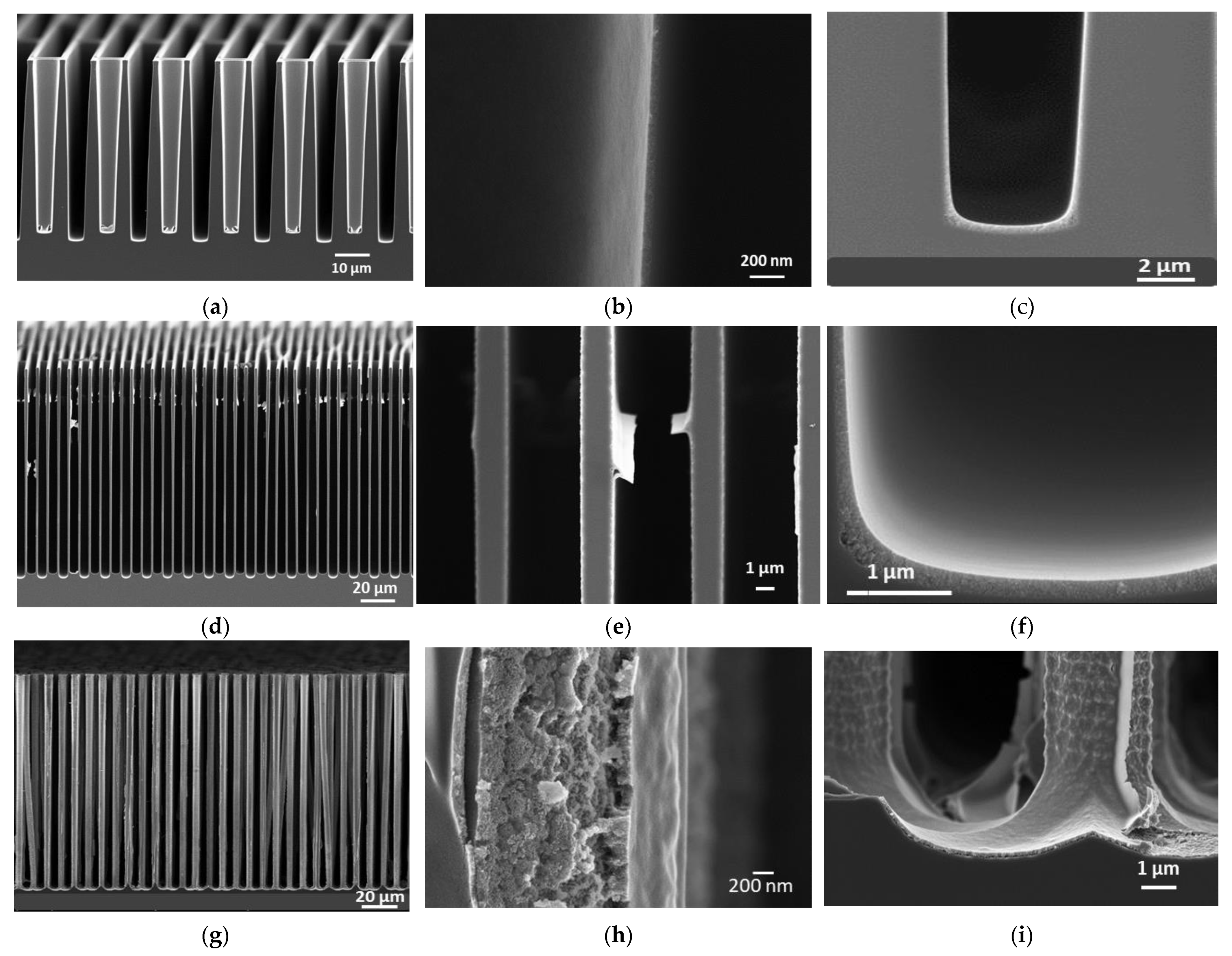
Figure 8.
(a) Cyclic voltammograms (second cycle) at 1 mV s−1 of 2D and 3D AR 29 TiO2 electrodes with 120 nm active material thickness (b) Surface capacity at different current densities for electrodes with a layer of 120 nm of TiO2 over 2D Si, 3D Si AR9 trenches, 3D Si AR29 trenches and 3D Si AR29 pillars subtracts.

Figure 9.
Surface capacitances as a function of the surface area enlargement factor. Black squares: experimental values; Red circles: theoretical values calculated from values obtained with 2D electrodes.
Figure 9.
Surface capacitances as a function of the surface area enlargement factor. Black squares: experimental values; Red circles: theoretical values calculated from values obtained with 2D electrodes.
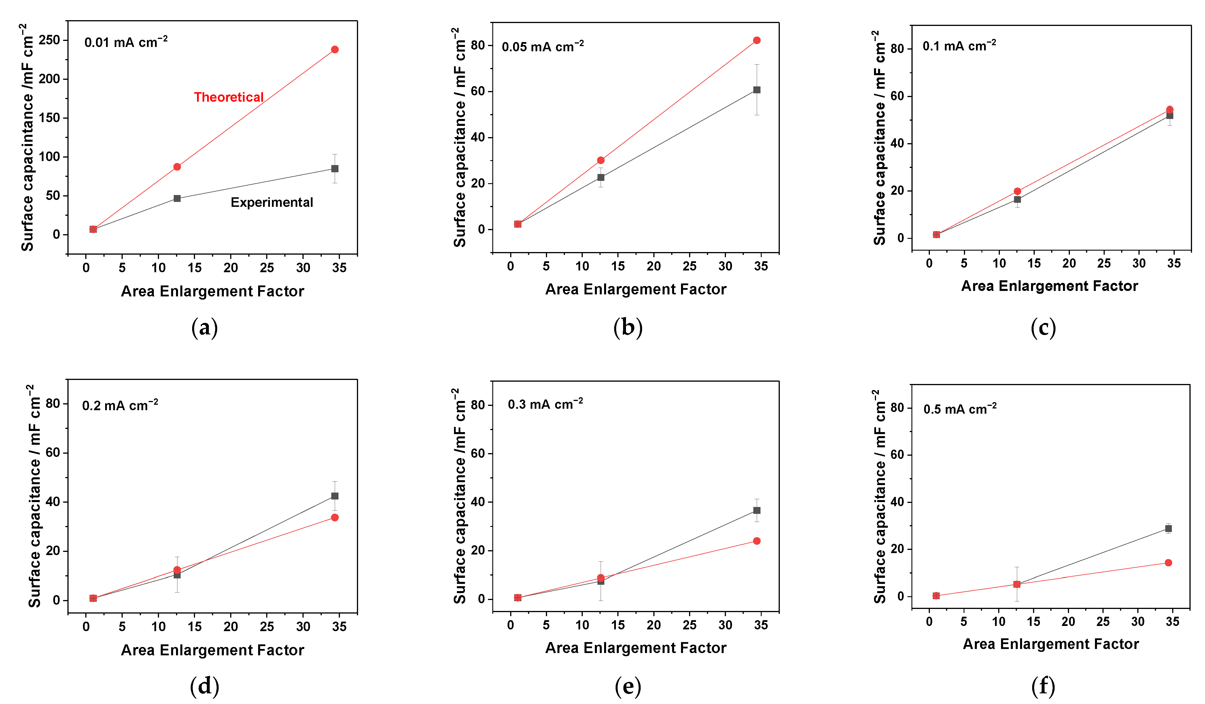
Figure 10.
Evolution of the surface capacitance for a 2D electrode with a 120 nm-thick TiO2 layer through galvanostatic charge–discharge cycles at a current density of 0.1 mA cm−2.
Figure 10.
Evolution of the surface capacitance for a 2D electrode with a 120 nm-thick TiO2 layer through galvanostatic charge–discharge cycles at a current density of 0.1 mA cm−2.

Table 1.
Dimensions and surface area enlargement for µtrench structures with aspect ratios 9 and 29 and µpillar structures with aspect ratio 29. The surface area enlargement presented in the table is calculated using Equations (1) and (2).
Table 1.
Dimensions and surface area enlargement for µtrench structures with aspect ratios 9 and 29 and µpillar structures with aspect ratio 29. The surface area enlargement presented in the table is calculated using Equations (1) and (2).
| Topology | Aspect Ratio | Etched Depth µm | Width µm | Spacing µm | Footprint Length cm | h µm | ν µm | Surface Area Enlargement |
|---|---|---|---|---|---|---|---|---|
| Trenches | 9 | 52 | 6 | 3 | 0.7 | - | - | 12.6 |
| Trenches | 29 | 117 | 4 | 3 | 0.7 | - | 34.4 | |
| Pillars | 29 | 144 | 5 | - | - | 9 | 8 | 32.4 |
Table 2.
Surface capacity at different current densities for electrodes with a layer of 120 nm of TiO2 over 2D Si, 3D Si AR9 trenches, 3D Si AR29 trenches and 3D Si AR29 pillars subtracts.
Table 2.
Surface capacity at different current densities for electrodes with a layer of 120 nm of TiO2 over 2D Si, 3D Si AR9 trenches, 3D Si AR29 trenches and 3D Si AR29 pillars subtracts.
| Current Density mA cm−2 | Surface Capacitance mF cm−2 | |||
|---|---|---|---|---|
| 2D | 3D AR9 Trenches | 3D AR29 Trenches | 3D AR29 Pillars | |
| 0.01 | 8.1 | 46.5 | 85.0 | 73.7 |
| 0.05 | 2.4 | 22.7 | 60.8 | 38.4 |
| 0.1 | 1.6 | 16.5 | 51.9 | 23.9 |
| 0.2 | 1.0 | 10.5 | 42.5 | 9.0 |
| 0.3 | 0.7 | 7.5 | 36.6 | 2.3 |
| 0.5 | 0.4 | 5.3 | 28.8 | 0.2 |
Disclaimer/Publisher’s Note: The statements, opinions and data contained in all publications are solely those of the individual author(s) and contributor(s) and not of MDPI and/or the editor(s). MDPI and/or the editor(s) disclaim responsibility for any injury to people or property resulting from any ideas, methods, instructions or products referred to in the content. |
© 2023 by the authors. Licensee MDPI, Basel, Switzerland. This article is an open access article distributed under the terms and conditions of the Creative Commons Attribution (CC BY) license (https://creativecommons.org/licenses/by/4.0/).
Share and Cite
MDPI and ACS Style
Poirot, N.; Gabard, M.; Boufnichel, M.; Omnée, R.; Raymundo-Piñero, E. Sustainable Approach for the Development of TiO2-Based 3D Electrodes for Microsupercapacitors. Batteries 2023, 9, 258. https://doi.org/10.3390/batteries9050258
AMA Style
Poirot N, Gabard M, Boufnichel M, Omnée R, Raymundo-Piñero E. Sustainable Approach for the Development of TiO2-Based 3D Electrodes for Microsupercapacitors. Batteries. 2023; 9(5):258. https://doi.org/10.3390/batteries9050258
Chicago/Turabian StylePoirot, Nathalie, Marie Gabard, Mohamed Boufnichel, Rachelle Omnée, and Encarnacion Raymundo-Piñero. 2023. "Sustainable Approach for the Development of TiO2-Based 3D Electrodes for Microsupercapacitors" Batteries 9, no. 5: 258. https://doi.org/10.3390/batteries9050258
Note that from the first issue of 2016, this journal uses article numbers instead of page numbers. See further details here.