Article

InAlGaN/GaN HEMTs at Cryogenic Temperatures

1
Institute of Electronics, Microelectronics and Nanotechnology (IEMN), Av. Poincaré, Villeneuve d’Ascq 59652, France
2
Centre de recherche sur les Ions, les MAtériaux et la Photonique, Caen 14000, France
3
Thales Research and Technology, 3-5lab, Av. Augustin Fresnel, RD128, Palaiseau 91767, France
*
Author to whom correspondence should be addressed.
Electronics 2016, 5(2), 31; https://doi.org/10.3390/electronics5020031
Submission received: 30 April 2016 / Revised: 8 June 2016 / Accepted: 17 June 2016 / Published: 22 June 2016
(This article belongs to the Special Issue Gallium Nitride Electronics)

Abstract

:
We report on the electron transport properties of two-dimensional electron gas confined in a quaternary barrier InAlGaN/AlN/GaN heterostructure down to cryogenic temperatures for the first time. A state-of-the-art electron mobility of 7340 cm2·V−1·s−1 combined with a sheet carrier density of 1.93 × 1013 cm−2 leading to a remarkably low sheet resistance of 44 Ω/□ are measured at 4 K. A strong improvement of Direct current (DC) and Radio frequency (RF) characteristics is observed at low temperatures. The excellent current and power gain cutoff frequencies (fT/fmax) of 65/180 GHz and 95/265 GHz at room temperature and 77 K, respectively, using a 0.12 μm technology confirmed the outstanding 2DEG properties.

1. Introduction

Al(In)GaN/GaN-based high-electron-mobility transistors (HEMTs) have shown great promise for high frequency and high power microwave applications owing to their highly conductive two dimensional electron gas (2DEG) combined with a high breakdown field. In order to achieve high-speed GaN devices, lattice-matched InAlN barrier layers were proposed, with which 2DEG carrier density is much higher than AlGaN barrier HEMTs, namely due to the spontaneous polarization [1,2]. However, the growth of InAlN is limited by the high immiscibility between AlN and InN, which results in alloy scattering and elevated interface roughness due to clustering in InAlN. Despite the implementation of an ultrathin AlN spacer to reduce the alloy scattering and enhance the 2DEG confinement [3], the growth of the ternary alloy remains challenging. On the other hand, a quaternary InAlGaN compound is attractive as a barrier layer since it allows easier adjustment of the band gap and strain state with suitable Al/In ratios [4,5,6,7,8,9,10]. Recently, we have reported InAlGaN/AlN/GaN heterostructure HEMTs with a sub-10-nm ultrathin quaternary barrier with a state-of-the-art electron mobility of 1800 cm2·V−1·s−1 and a sheet carrier density of 1.9 × 1013 cm−2 at room temperature [11]. In this paper, the 2DEG properties of this specific heterostructure are investigated for a temperature range of 4–400 K. Furthermore, InAlGaN/AlN/GaN HEMTs using 120 nm gate lengths (LG) have been fabricated and characterized at room temperature (RT) and low temperature (77K).

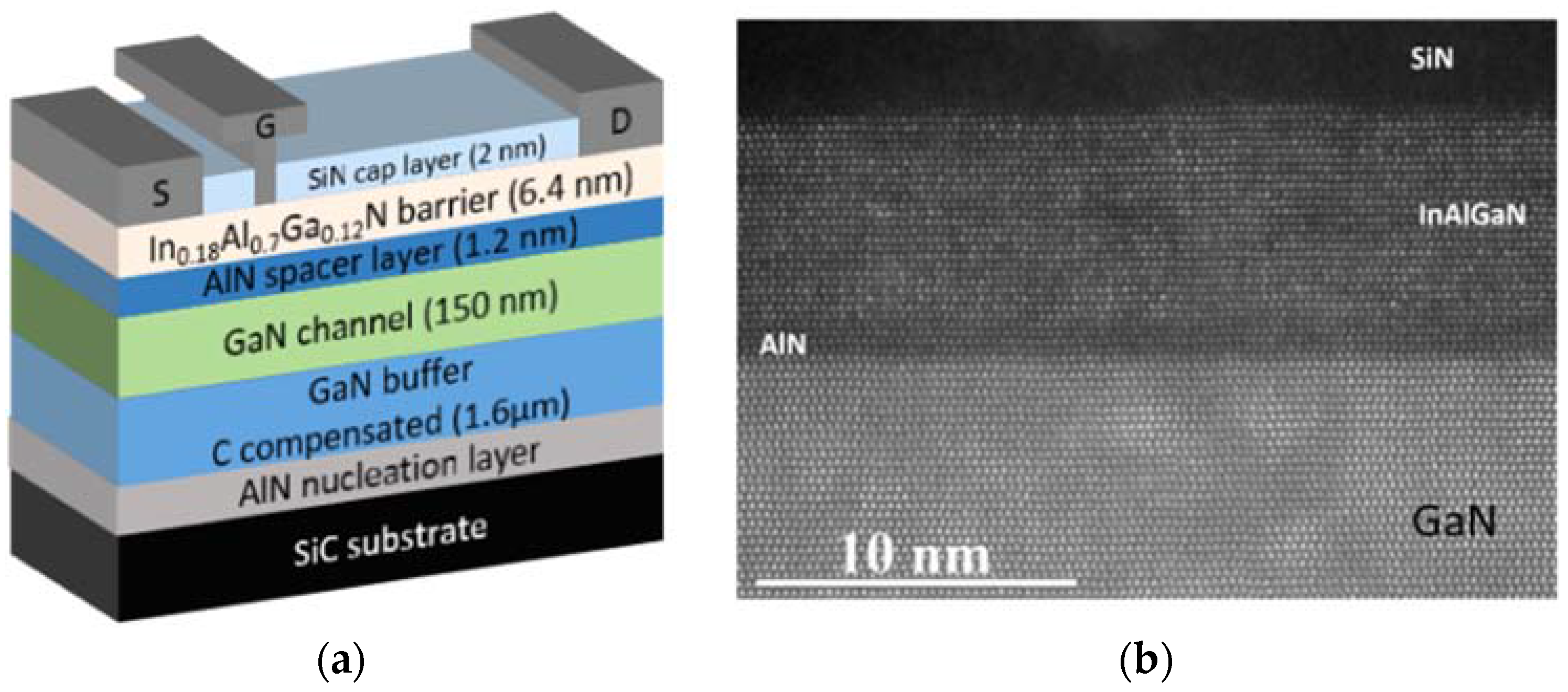
2. Device Fabrication

The structure was grown by low-pressure metal–organic chemical vapor deposition (MOCVD) on a 4 in SiC substrate and consists of a 1.6 µm carbon compensated buffer layer, a 150-nm-thick GaN channel, a 1.2-nm-thick AlN interlayer, a 6.4-nm-thick In0.18Al0.70Ga0.12N layer and a 2-nm-thick in situ SiN cap layer (Figure 1a). Transmission electron microscopy (TEM) analysis revealed a high quality two-dimensional growth of the InAlGaN and AlN layers on GaN with smooth interfaces as can be seen in Figure 1b. Details on growth conditions and further structural characterizations of the SixNy/InAlGaN/AlN/GaN HEMT heterostructure can be found elsewhere [11].

3. Results

Cryogenic temperature Hall effect measurements were assessed in a vacuum chamber by using a helium gas closed-cycle cryostat and Lakeshore 776HMS measurement system. Figure 2 shows the Hall electron mobility, sheet carrier density and sheet resistance of the HEMT structure over the 4–400 K range. At liquid helium temperature (4 K), a state-of-the-art 2DEG mobility of 7340 cm2·V−1·s−1 combined with a sheet carrier density of 1.93 × 1013 cm−2 was measured, resulting in a remarkably low sheet resistance of 44 Ω/□. For InAlN/AlN/GaN heterostructures, the carrier mobility was reported to be determined by a temperature-independent interface roughness scattering mechanism, while above 200 K the optical and acoustical phonon scattering become dominant [12]. Consequently, in this study, the excellent combination of electron mobility and a high 2DEG carrier density below 200 K is attributed to very low interface roughness and optimized quaternary alloy barrier thickness. Furthermore, the in situ SixNy cap layer, which provides handling strain relaxation as well as serving as an early surface passivation layer, enhances the 2DEG properties.
In order to emphasize the effect of crystalline quality on 2DEG properties, Table 1 presents a comparison of room-temperature 2DEG characteristics of the SixNy/InAlGaN/AlN/GaN heterostructures with similar designs grown on SiC and sapphire substrates. Higher electron mobility and sheet carrier density yielding much lower sheet resistance is observed for the HEMT structure grown on SiC compared to those on sapphire. The better epitaxial growth quality is attributed to the lower defect density and higher thermal conductivity [13].
SixNy/InAlGaN/AlN/GaN HEMTs grown on SiC were fabricated using a gate length of 120 nm in order to reflect the remarkable 2DEG characteristics. Device processing has been performed by using a Ti/Al/Ni/Au metal stack for ohmic contacts on an InAlGaN barrier followed by a rapid thermal annealing at 875 °C, resulting in contact resistances of 0.4 Ω·mm. T-shaped Ni/Au gate Schottky contacts were defined by e-beam lithography. Nitrogen quadruple implantation (20 keV, 50 keV, 100 keV and 150 keV) was used for device isolation. A 0.3 µm gate-source and 2 μm gate–drain spacing were employed with a gate width of 50 μm.

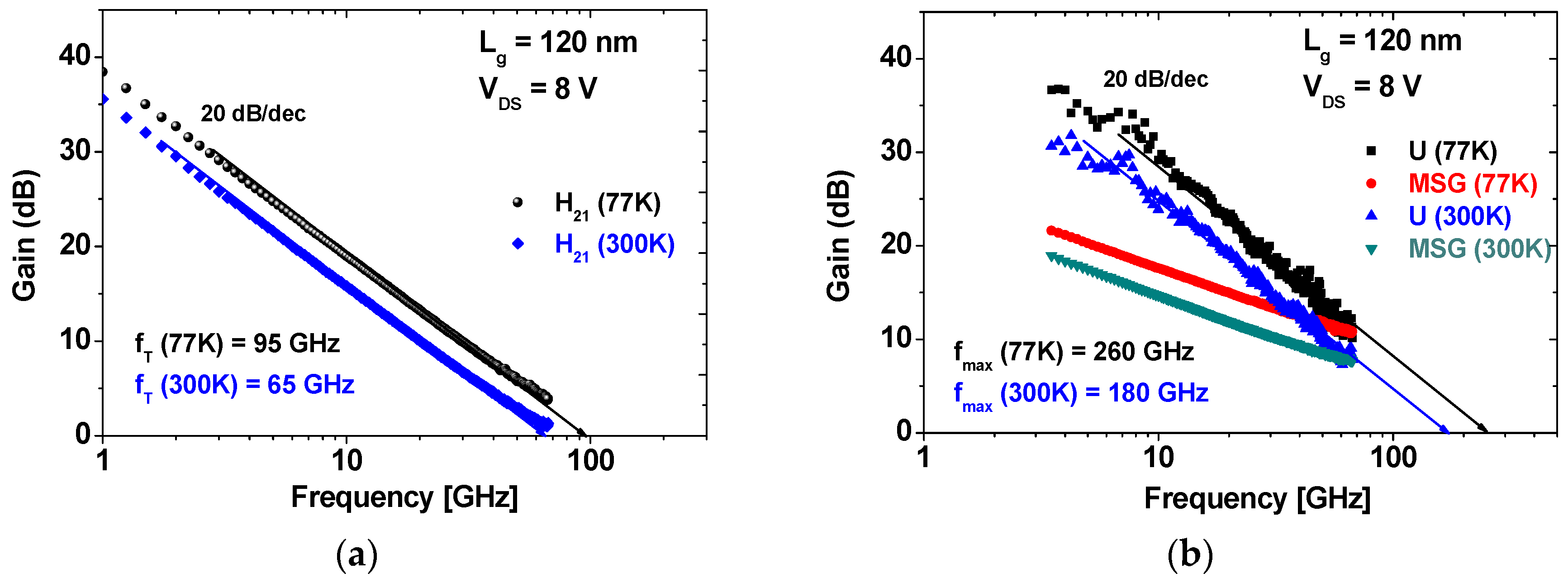
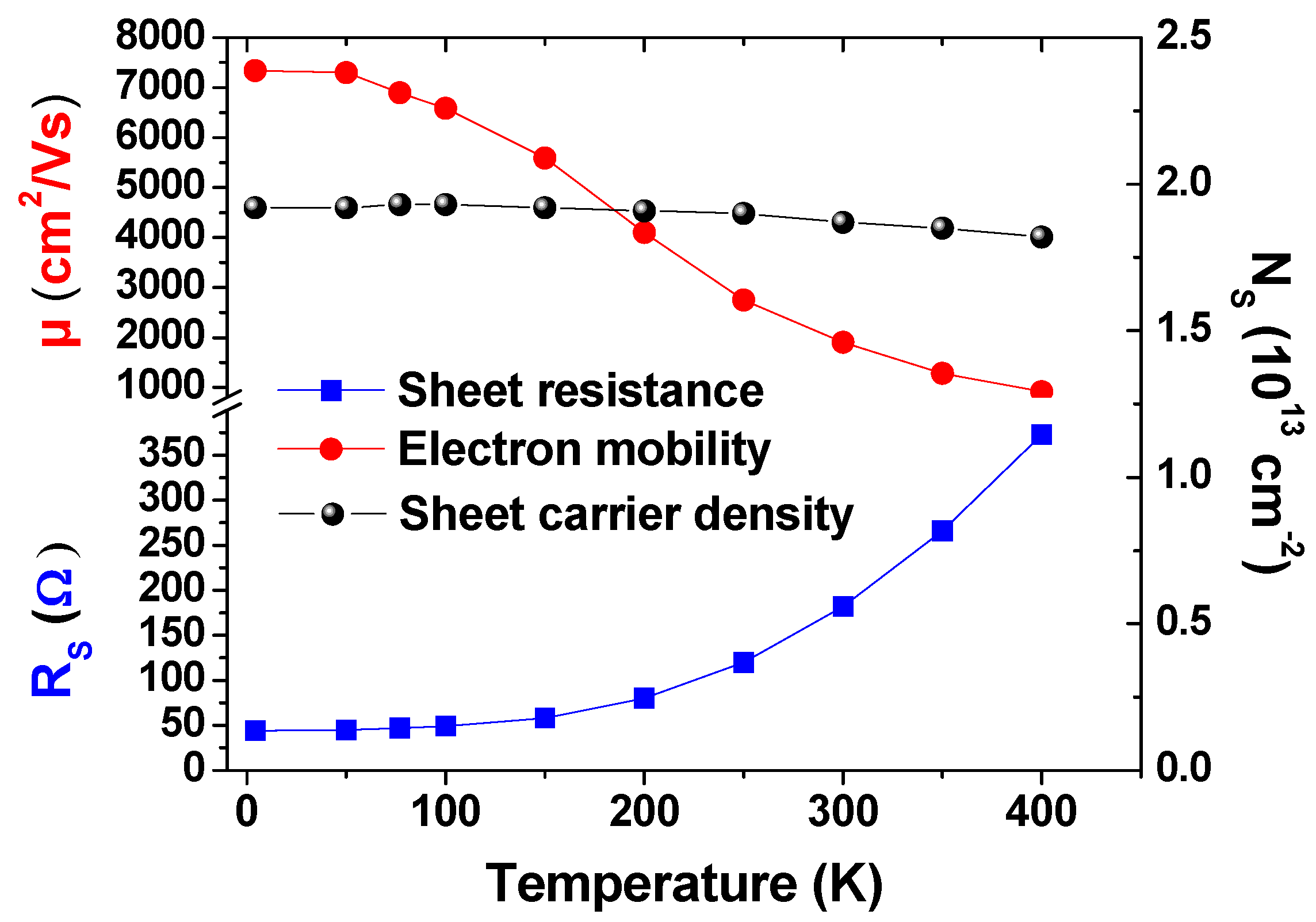
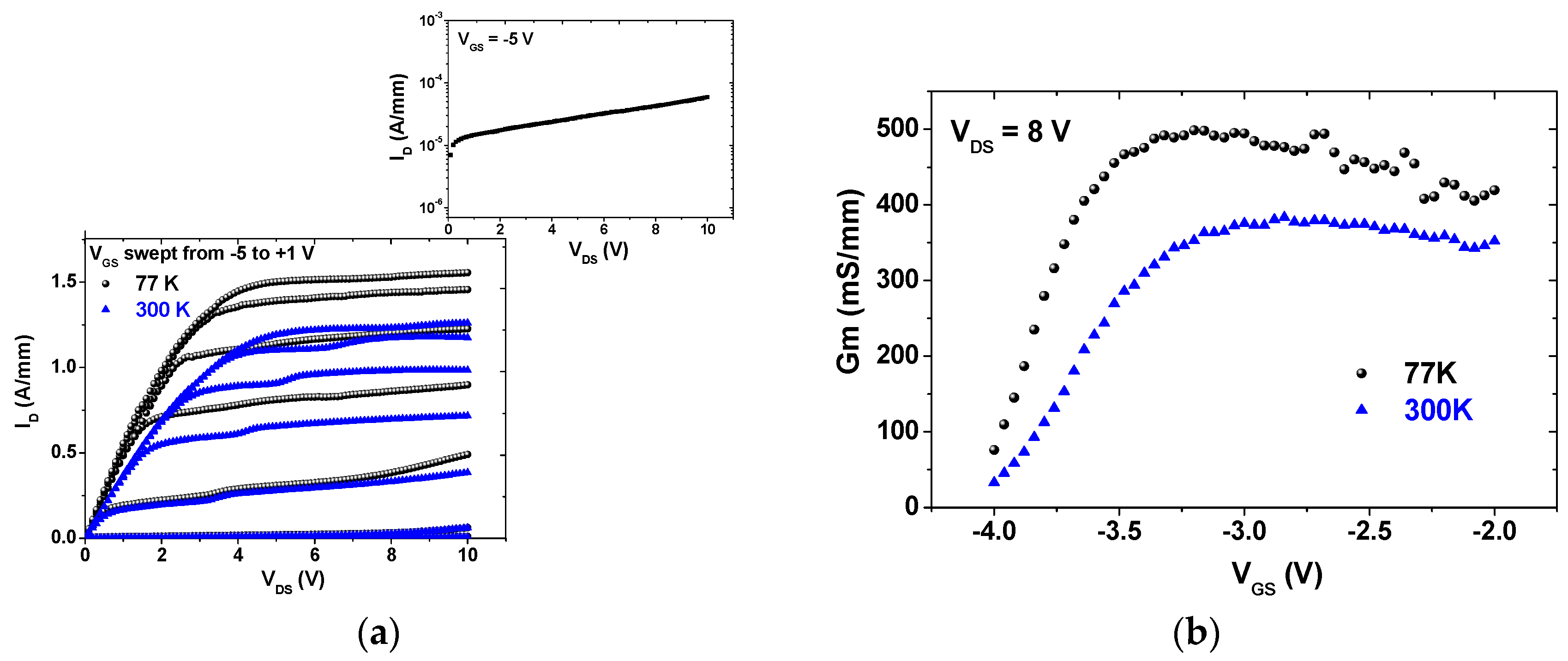
DC and RF Characteristics at RT and 77K

Agilent E5273A and E8361A network analyzers were used in order to assess the cryogenic temperature DC and RF characteristics of the HEMT devices in a vacuumed cryogenic probing system equipped with a nitrogen gas closed-cycle cryostat and on-wafer probes. The drain current-voltage and transfer characteristics of a 0.12 × 50 μm2 InAlGaN/GaN HEMT at 77 K and RT are presented in Figure 3. The saturated DC output current density at VGS = +1 V increased from 1.3 A/mm to 1.6 A/mm as the operation temperature decreased from RT to 77 K as shown in Figure 3a. In addition, at 77 K the on-resistance (RON) decreased by 20% relative to its RT value. Similarly, at 77 K the extrinsic transconductance (gm,ext) peak showed an increase of about 40% from its RT value and reached 500 mS/mm (Figure 3b). As a matter of fact, the improvement in 2DEG mobility and the decrease in sheet resistance from RT to 77 K, leading to an effective increase of the electron velocity under the gate, results in enhanced DC characteristics at lower operation temperature [14].
Figure 4a,b reveal the current-gain (fT) and power-gain (fmax) extrinsic cut-off frequencies at RT and 77 K extrapolated from the current gain H21 and the unilateral power gain U at VGS = −3 V and VDS = 8 V, respectively. The values of fT/fmax were derived to be 65/180 GHz and 95/265 GHz at RT and 77 K, respectively. The frequency performances are clearly limited by the parasitic access resistances and thus ohmic contact resistances should be decreased in order to achieve higher cut-off frequencies.
The increase in both fT and fmax at 77 K is in good agreement with the transfer characteristics in Figure 3 as well as the studies reporting on low temperature behavior of GaN-based HEMTs in the literature [15,16]. It can be pointed out that RF performances are mainly limited by the access resistances due to rather high parasitic contact resistances.

4. Conclusions

Sub-10-nm ultrathin quaternary barrier In0.18Al0.70Ga0.12N/AlN/GaN HEMTs capped with an in situ SixNy revealed a smooth surface and high crystalline quality. Record 2DEG mobilities of 1800 cm2V−1·s−1 at RT and 7340 cm2V−1·s−1 at 4 K were achieved with a remarkably high carrier sheet density of 1.9 × 1013 cm−2. The very high electron mobility in this ultrathin barrier heterostructure over the 4–400 K range is attributed to the reduced interface roughness owing to the implementation of an optimized AlN spacer layer and the use of an in situ–grown SixNy cap layer. The DC and RF characteristics of the fabricated HEMT at 77 K reflected the outstanding high 2DEG electron mobility and very low sheet resistance at low temperature operation.

Acknowledgments

This work was supported by the French Defense Procurement Agency (DGA) under project EDA-EuGaNiC (European Defense Agency), the French RENATECH network and the National Research Agency under contract ANR-14-CE26-0022 (LHOM).

Author Contributions

P. Gamarra, C. Lacam, M. Tordjman have grown the epilayers; E. Dogmus, R. Kabouche, S. Lepilliet, A. Linge, M. Zegaoui, and F. Medjdoub conceived, designed and performed the experiments; Hichem Ben-Ammar, Marie-Pierre Chauvat, P. Ruterana have performed the material analysis and TEM images.

Conflicts of Interest

The authors declare no conflict of interest.

References

  1. Kuzmik, J. Power electronics on InAlN/(In)GaN: Prospect for a record performance. IEEE Electron Device Lett. 2001, 22, 510. [Google Scholar] [CrossRef]
  2. Kohn, E.; Medjdoub, F. InAlN—A new barrier material for GaN-based HEMTs. In Proceedings of the International Workshop on Physics of Semiconductor Devices, 2007, Mumbai, India, 16–20 December 2007; pp. 311–316.
  3. Gonschorek, M.; Carlin, J.F.; Feltin, E.; Py, M.A.; Grandjean, N. High electron mobility lattice-matched AlInN/GaN field-effect transistor heterostructures. Appl. Phys. Lett. 2006, 89, 062106. [Google Scholar] [CrossRef]
  4. Liu, Y.; Egawa, T.; Jiang, H. Enhancement-mode quaternary AlInGaN/GaN HEMT with non-recessed-gate on sapphire substrate. IEEE Electron Device Lett. 2006, 42, 884–886. [Google Scholar] [CrossRef]
  5. Makiyama, K.; Ozaki, S.; Ohki, T.; Okamoto, N.; Minoura, Y.; Niida, Y.; Kamada, Y.; Joshin, K.; Watanabe, K.; Miyamoto, Y. Collapse-free high power InAlGaN/GaN-HEMT with 3 W/mm at 96 GHz. In Proceedings of the 2015 IEEE International Electron Devices Meeting (IEDM), Washington, DC, USA, 7–9 December 2015; pp. 9.1.1–9.1.4.
  6. Gao, X.; Pan, M.; Gorka, D.; Oliver, M.; Schuette, M.; Ketterson, A.; Saunier, P. Ultra-thin barrier quaternary InAlGaN HEMTs with state of the art sheet resistance. Phys. Status Solidi C 2014, 11, 495–497. [Google Scholar] [CrossRef]
  7. Hwang, J.H.; Kim, S.; Woo, J.M.; Hong, S.; Jang, J.-H. GaN HEMTs with quaternary In0.05Al0.75Ga0.2N Schottky barrier layer. Phys. Status Solidi C 2016, 213, 889–892. [Google Scholar] [CrossRef]
  8. Ketteniss, N.; Khoshroo, L.R.; Eickelkamp, M.; Heuken, M.; Kalisch, H.; Jansen, R.H.; Vescan, A. Study on quaternary AlInGaN/GaN HFETs grown on sapphire substrates. Semicond. Sci. Technol. 2010, 25, 055012. [Google Scholar] [CrossRef]
  9. Wang, R.; Li, G.; Verma, J.; Sensale-Rodriguez, B.; Fang, T.; Guo, J.; Hu, Z.; Laboutin, O.; Cao, Y.; Johnson, W.; et al. 220-GHz Quaternary Barrier InAlGaN/AlN/GaN HEMTs. IEEE Electron Device Lett. 2011, 32, 1215–1217. [Google Scholar] [CrossRef]
  10. Lim, T.; Aidam, R.; Waltereit, P.; Henkel, T.; Quay, R.; Lozar, R.; Maier, T.; Kirste, L.; Ambacher, O. GaN-based submicrometer HEMTs with lattice-matched InAlGaN barrier grown by MBE. IEEE Electron Device Lett. 2010, 31, 671–673. [Google Scholar] [CrossRef]
  11. Medjdoub, F.; Kabouche, R.; Linge, A.; Grimbert, B.; Zegaoui, M.; Gamarra, P.; Lacam, C.; Tordjman, M.; Forte-Poisson, M.F. High electron mobility in high-polarization sub-10 nm barrier thickness InAlGaN/GaN heterostructure. Appl. Phys. Express 2015, 8, 101001. [Google Scholar] [CrossRef]
  12. Tulek, R.; Iygaz, A.; Gokden, S.; Teke, A.; Ozturk, M.K.; Kasap, M. Comparison of the transport properties of high quality AlGaN/AlN/GaN and AlInN/AlN/GaN two-dimensional electron gas heterostructures. J. Appl. Phys. 2009, 105, 13706. [Google Scholar] [CrossRef] [Green Version]
  13. Wu, Y.F.; Kapolnek, D.; Ibbetson, J.P.; Parikh, P.; Keller, B.P.; Mishra, U.K. Very-High Power Density AlGaN/GaN HEMTs. IEEE Trans. Electron. Devices 2001, 48, 586–590. [Google Scholar]
  14. Endoh, A.; Watanabe, I.; Yamashita1, Y.; Mimura, T.; Matsui, T. Effect of temperature on cryogenic characteristics of AlGaN/GaN MIS-HEMTS. Phys. Status Solidi C 2009, 6, S964–S967. [Google Scholar] [CrossRef]
  15. Sensale-Rodriguez, B.; Guo, J.; Wang, R.; Verma, J.; Li, G.; Fang, T.; Beam, E.; Ketterson, A.; Schuette, M.; Saunier, P.; et al. Time delay analysis in high speed gate-recessed E-mode InAlN HEMTs. Solid-State Electron. 2013, 80, 67–71. [Google Scholar] [CrossRef]
  16. Xue-Feng, Z.; Li, W.; Jie, L.; Lai, W.; Jian, X. Electrical characteristics of AlInN/GaN HEMTs under cryogenic operation. Chin. Phys. B 2013, 22, 017202. [Google Scholar]
Figure 1. Schematic cross-section (a) and TEM image (b) of SixNy/InAlGaN/AlN/GaN HEMTs.
Electronics 05 00031 g001
Figure 2. Sheet resistance (in blue), Hall mobility (in red) and sheet carrier density (in black) of the SixNy/InAlGaN/AlN/GaN HEMT heterostructure as a function of temperature.
Electronics 05 00031 g002
Figure 3. ID-VDS characteristics (the inset shows the sub-threshold behavior up to 10 V in semi-log scale) (a) and transfer characteristics (b) of 0.12 × 50 µm2 AlInGaN/GaN HEMTs at RT (in blue) and 77 K (in black).
Electronics 05 00031 g003
Figure 4. Current-gain (Figure 4a) and power-gain cut-off frequency (Figure 4b) at VDS = 8 V of a 0.12 × 50 µm2 AlInGaN/GaN HEMTs at RT (in blue) and 77 K (in black).
Electronics 05 00031 g004
Table 1. Comparison of room temperature 2DEG properties of the SixNy/InAlGaN/AlN/GaN heterostructures with similar designs grown on sapphire and SiC substrates.
SubstrateElectron Mobility (cm2·V−1·s−1)Sheet Carrier Density (cm−2)Sheet Resistance (Ω/□)
Sapphire10601.74 × 1013340
SiC18001.93 × 1013191

