1. Introduction
Organic field-effect transistors (OFET) are the key devices for the development of complex analog and digital electronic circuits which, based on low-temperature processed organic semiconductors, can be fabricated through cost-effective techniques [
1]. Nowadays, owing to the results of a wide number of accurate experiments, we are fully aware that the quality of the electrical response of an OFET basically relies on the robustness of the charge transport processes taking place across and along the interfaces separating the different device component parts. In particular, severe effects of contact resistance can strongly compromise the device behavior in the presence of a non-optimized charge injection condition. With regard to this last phenomenon, it can be largely dependent on the matching of the Fermi level of the injecting electrode and the LUMO (Low Unoccupied Molecular Orbital) or HOMO (High Occupied Molecular Orbital) level of the organic semiconductor, as well as on the morphological order of the active channel in the proximity of the metal contact [
2].
At the same time, a crucial role is also played by the interface between the dielectric barrier and the organic channel, where the charge motion occurs in a very thin region involving few molecular layers [
3]. Starting from this consideration, it becomes clear that the chemical and physical nature of the dielectric/organic interface impacts extraordinarily on the final device performances, with the possible occurrence of trapping processes, limiting the carrier mobility and contemporarily giving rise to hysteresis and/or bias-stress effects (namely, the change over time of the drain-source I
DS current when the device is driven in the accumulation regime) [
4,
5].
In the recent past, time and spatial resolved scanning Kelvin probe microscopy (SKPM) allowed us to gain detailed information about the basic mechanisms ruling the charge transport in the OFET [
6]. In this context, specific attention was devoted to processes like trapping energy [
7], dynamics of trapping and detrapping [
8], charge injection at the electrodes [
9,
10] and charge recombination mechanisms [
11]. The near totality of these reports was focused on p-type (hole-transporting) organic transistors, while very little experimental data concerning SKPM experiments performed on n-type (electron-transporting) OFET are still available today [
12]. This occurrence is basically due to the slowness with which organic semiconductors, displaying reliable electron-accumulation effects, have been developed with respect to p-type compounds. Indeed, considerable research has been necessary to synthesize conjugated compounds with contemporarily good self-assembling properties and large electron affinity, thus making the formation of radical anions possible, with sufficient insensitivity to oxidative processes by the ambient gases. In particular, within the last 10 years, Perylene diimide molecules functionalized with cyano groups in the bay regions (PDI_CY) have emerged as a new class of n-type organic semiconductors, with highly stable electrical performances under ambient conditions and effective charge injection from gold electrodes [
13,
14]. All these features are basically triggered by the low-lying LUMO levels (down to −4.5 eV) of these compounds, which come from the presence of strong electron-withdrawing moieties in their molecular structure.
Among the PDI_CY molecules,
N,
N0-1
H,1
H-perfluorobutyl-cyanoperylenediimide (PDIF-CN
2) is the compound displaying the highest electron mobility (µ) both in form of thin film [
15,
16] and single crystal [
17,
18]. In particular, PDIF-CN
2 single-crystal devices have demonstrated µ values up to 6 cm
2/Volt·s, band-like transport features (namely, µ increases in a range of temperatures below room temperature) [
19] and negligible bias stress effects [
20]. On the other hand, very recently, PDIF-CN
2 thin-film transistors have also been shown to be able to operate steadily in aqueous environments, opening a new perspective for the use of this compound in the development of bio-sensing devices [
21].
In this paper, we analyze the morphological and electrical properties of PDIF-CN2 films deposited by Joule evaporation from Knudsen cells on SiO2 substrates with different surface properties. Our results clearly highlight that the self-assembling properties of PDIF-CN2 molecules and the related electrical performances are strongly improved when hydrophobic surfaces are used for the film growth. SKPM was then applied to investigate basic aspects concerning the charge injection process in the PDIF-CN2 films and the poor operational stability of these devices when operated for a prolonged time in the depletion regime.
3. Results and Discussion
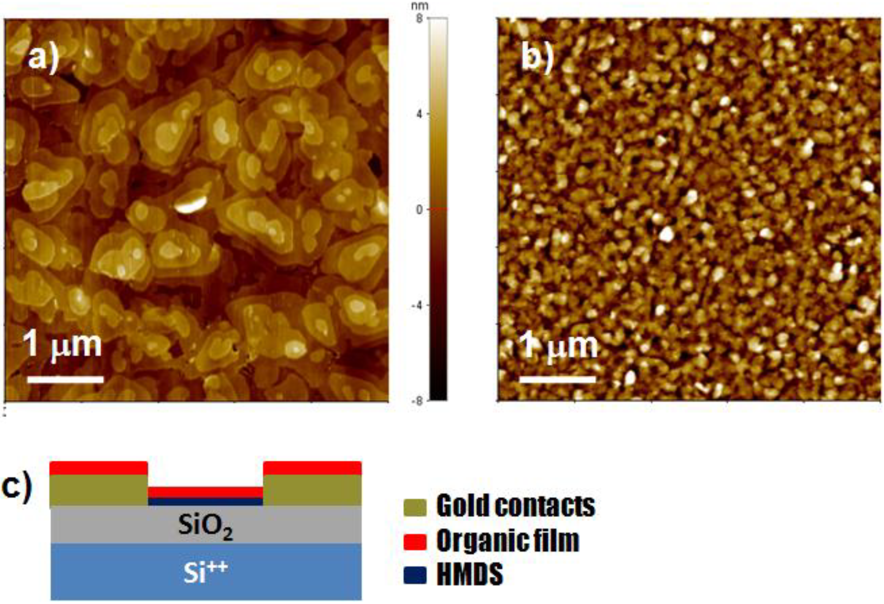
AFM images in
Figure 1 report the surface morphology of PDIF-CN
2 films evaporated on bare and HMDS-treated substrates, setting the substrate temperature (
Tsub) at 90 °C. As shown, the film microstructure is strongly affected by the SiO
2 functionalization. In particular, on the bare substrates (
Figure 1b), the films show a poor morphological order, being composed of small and rounded grains with a lateral size lower than 100 nm. On the other hand, on HMDS substrates (
Figure 1a), the long-range order appears to be considerably improved and the films are characterized by the presence of larger circular islands, with diameters approaching 1 µm in the best cases. Moreover, the film surface displays a well-defined terraced structure with molecular steps close to 2 nm, in agreement with previous reports [
25], which may indicate an alignment of the long axis of the molecules close to the direction perpendicular to the substrate.
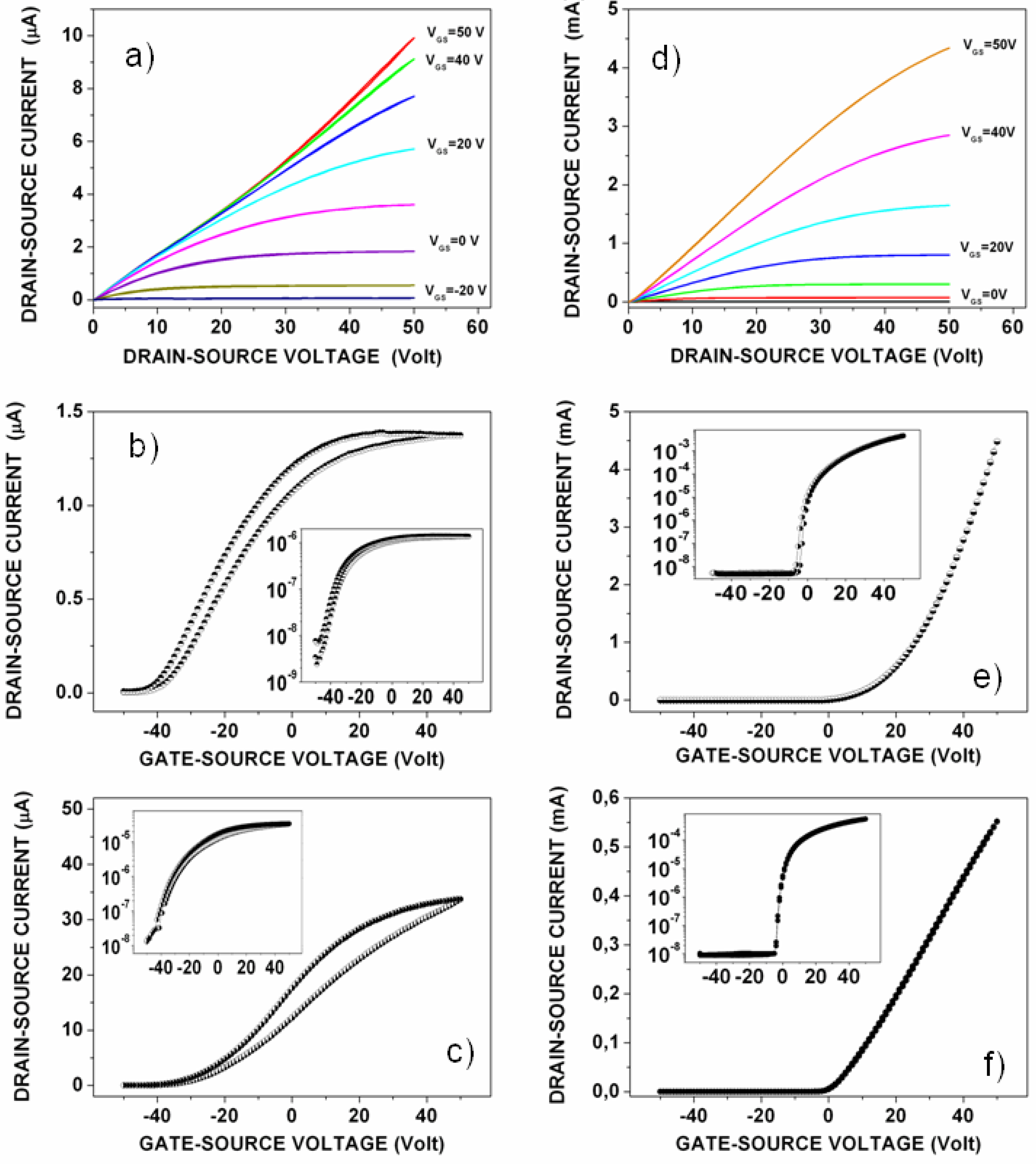
The electrical responses measured for the PDIF-CN
2 transistors demonstrate a clear correlation between the film morphological properties and the related charge transport performance. First of all, the output curves reported in
Figure 2a for a PDIF-CN
2 transistor fabricated on bare SiO
2 substrate, evidence the occurrence of peculiar and not ideal electrical features. Indeed, although the current behavior in the low V
DS (<10 V) region seems apparently linear, all the I
DS current curves overlap for V
GS higher than 10 V and no further current modulation is observable.
Figure 2.
(a) Output curves and transfer-curves in (b) linear (VDS = 5 V) and (c) saturation regions (VDS = 50 V) for a PDIF-CN2 transistor deposited on bare SiO2 substrate. (d) Output curves and transfer-curves in (e) linear (VDS = 5 V) and (f) saturation (VDS = 50 V) regions for a PDIF-CN2 transistor deposited on HMDS-treated SiO2 substrate. In the insets, we show data in a semi-log plot where the current scale is Ampere and the voltage scale is Volt.
The transfer-curves reported in
Figure 2b,c in the linear and saturation regimes, respectively, confirm the poor electrical performances of this class of devices. In particular, besides the presence of a large hysteresis, the transfer-curve in the linear regime again makes clear that, under the application of small
VDS voltages and for
VGS exceeding 10 V, the device is not able to work properly, since the I
DS current reaches a constant value that V
GS is no longer able to modulate.
The inability to further control the channel conductance could be ascribed to the detrimental action of very large contact resistances (
RC) at the source and drain electrodes, which, because of their weak dependence on
VGS, are able to completely dominate the device electrical response in the full accumulation region [
26,
27,
28].
To find an experimental confirmation regarding the
RC role in the electrical behavior of these PDIF-CN
2 transistors, we carried out SKPM measurements acquiring the potential profile along a line across the channel of the device in operation with
VGS grounded and
VDS < 10 V (in the specific, 4.5 Volt for not treated device and 7 Volt for the HMDS-treated one). In these driving conditions, the device works in the linear regime (see the output curve at
VGS = 0 V in
Figure 2a).
Figure 3 depicts the measured potential profile in the transistor channel. As shown, while the potential follows the predicted linear behavior in the central part of the channel, a large drop (Δ
VS ~ 1.4 V) appears in the film region (about 2 µm long) close the source electrode. In contrast, only a very small drop of about Δ
VD ~ 0.1 V can be detected near the drain electrode. This experimental finding reveals that the contact resistance effect is related exclusively to the charge injection process taking place at the source contact and, hence, the
RC value can be simply evaluated by dividing (Δ
VS) for the current flowing in the channel (
IDS = 0.44 μA), achieving about 3 MΩ. This value seems to confirm the idea that the device resistance (usually in the range between 3 and 5 MΩ) measured in the V
GS-independent current region (
VGS > 10 V in the transfer-curves), as reported in
Figure 2, is completely determined by the contact resistance contribution.
Figure 3.
Surface potential profile measured by scanning Kelvin probe microscopy (SKPM) across the channel. The colored areas indicate drain (blue light) and source (red light) contacts.
Figure 3.
Surface potential profile measured by scanning Kelvin probe microscopy (SKPM) across the channel. The colored areas indicate drain (blue light) and source (red light) contacts.
In the saturation regime, the role of contact resistance is still clearly visible and the related transfer-curve shows that the I
DS slope strongly reduces at increasing
VGS. Here, the maximum trans-conductance (g
m = ∂I
DS/∂V
GS) does not exceed 0.8 μS, while a rough estimation of the charge carrier mobility using the MOSFET equations gives a value of 0.002 cm
2/Volt·s. Significantly (see the semi-log plots in the inset of
Figure 2b,c), the I
DS starts flowing in the channel for highly negative V
GS, usually comprised between −30 V and −40 V. These V
GS values are usually defined as the onset voltages (
Von) of the transistor and, for PDIF-CN
2 films on bare SiO
2 substrates, they are even more negative than the corresponding values measured for the parent compound PDI8-CN
2 on the same type of SiO
2 surface [
29]. This occurrence supports the hypothesis that the negative
Von in the PDI_CY-based transistors is related to unintentional charge doping effects given by the interaction between the perylene molecules and water molecules absorbed on the substrate surface [
29,
30]. On the basis of this concept, the larger the electron affinity of the n-type compounds the more negative will be the
Von values.
Due to the improved morphological order, PDIF-CN
2 transistors fabricated on HMDS-treated substrates exhibit noticeably improved electrical performances (
Figure 2d,e,f), and no potential drop related to the R
C effects is appreciable in the SKPM profile reported in
Figure 3. In general, the electrical behavior of these devices follows the predictions of the ideal MOSFET model very closely, with the absence of significant hysteresis phenomena.
Mobility values extracted from the curves in the saturation regime are distributed on a homogeneous set of 23 samples, around a mean value of (0.37 ± 0.19) cm
2/Volt·s. For one device, we measured a mobility of 0.71 cm
2/Volt·s which exceeds the highest value ever reported for an evaporated PDIF-CN
2 thin-film transistor [
13]. In several cases, the maximum I
DS current measured in the saturation regime was higher than 4 mA, while the trans-conductance (g
m) came close to the value of 0.2 mS in the best case. It is significant to outline that, according to the experimental data so far reported in literature, mobility values higher than 0.3 cm
2/Volt·s have been measured only for films evaporated with
Tsub ~ 130 °C [
14]. Since this temperature is considerably higher than that (
Tsub = 90 °C) used in this work, we consider that the mobility enhancement obtained in our growth conditions is basically due to the quality of the adopted HMDS treatment, making the SiO
2 surface highly hydrophobic with a water contact angle θ
c close to 110°. The impact of the HMDS surface coverage level on the response of the final transistor was already stressed in [
14]. Considering the effect of the SiO
2 functionalization on the electrical behavior of the analyzed PDIF-CN
2 transistors, it can be also concluded that the contact resistance effect observed for the devices fabricated on bare substrates must be mainly related to the poor structural order of the related films. However, a degradation effect of the injection process, associated to the water electrolysis phenomenon occurring on the metallic surface of the gold source electrode and the consequent protonization of the silanol groups on silicon surface closed to the source electrode, cannot be excluded [
4].
Besides the strong influence on mobility and R
C effects, HMDS-treatment also provided a
Von shift toward the ideal 0 V, similar to what had recently been observed for PDI8-CN
2 devices [
29]. This evidence is in agreement with the aforementioned discussion about the role of water molecules absorbed on the SiO
2 surface in the
Von determination. For most of the pristine PDIF-CN
2 devices on HMDS,
Von was found to range between −10 and −5 V. However, we also observed that these values can be largely modified during the device operation and, in particular, when the transfer-curves are recorded continuously in air for long periods. More specifically, it was found that a prolonged application of negative
VGS voltages is able to induce a considerable shift of the
Von values towards more negative values. This phenomenon had already been reported for PDI8-CN
2 inkjet-printed OFET and is probably common to n-type devices based on organic semiconductors which have a large electron affinity [
30].
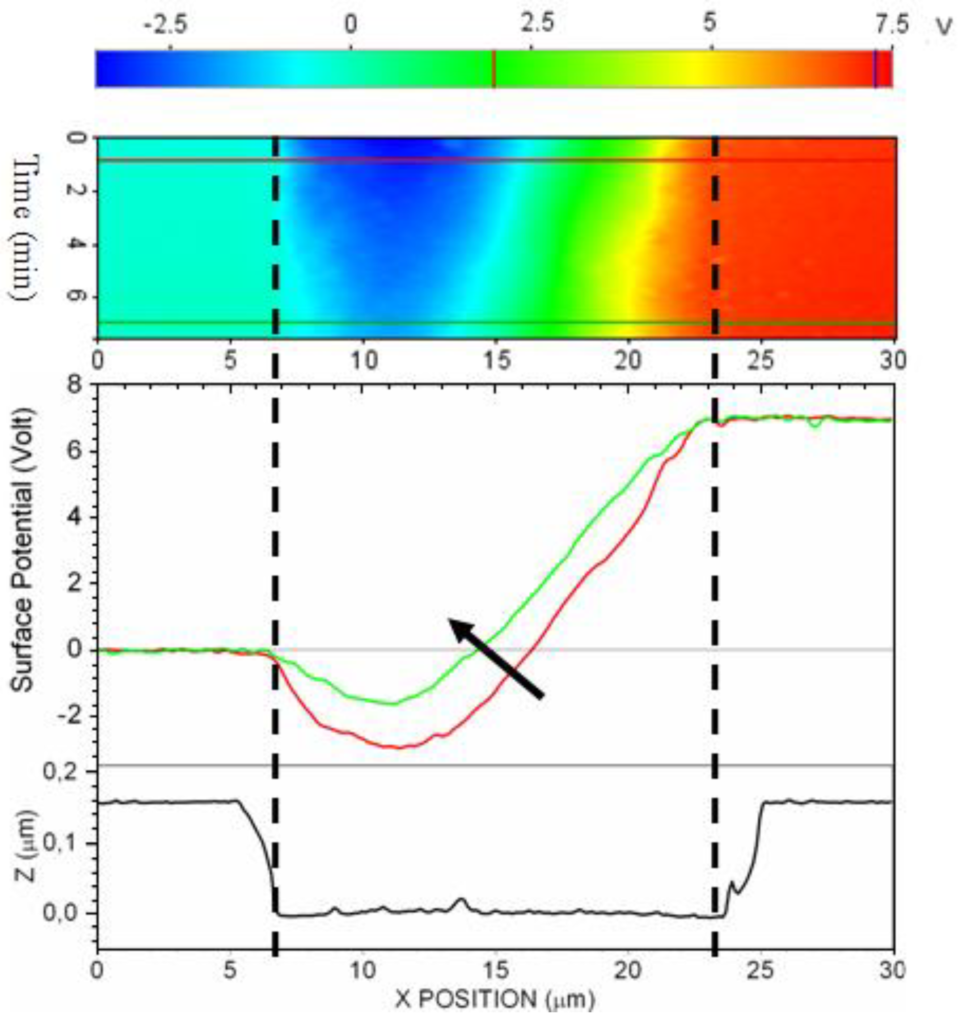
Figure 4.
(top panel) Time evolution of the potential along a line across the channel, the upper bar is the chromatic scale for the potential values; (middle panel) graph of potential of two specific lines at the beginning (red lines) and the end (green lines) of the experiment, the arrow indicates increasing time; (bottom panel) topographic profile of the channel acquired contemporarily with potentiometric measure. Vertical dashed lines are guides for eyes to indicate where the gold contacts finish.
While the effect of a continuous application of
VGS (positive for n-type OFET) driving the devices into the accumulation regime (
i.e., the so-called bias stress effect) can be analyzed in a direct manner through the observation of the
IDS(
t) behavior, it becomes much more difficult to investigate the time evolution of the device response in the depletion regime, where the
IDS current is very low. To approach this interesting task, we have performed SKPM with
VGS = −20 V and
VDS = 7.5 V along a line across the channel for a time of 10 min. We observe (
Figure 4) the presence of a vale in the potential profile inhibiting electron injection for this n-type device. As shown, this potential well gradually tends to disappear over the time scale of ten minutes, causing the device to move from the depletion regime to that of accumulation and the consequent
Von shift. We observe that this time is much shorter than the typical time of recovery as already observed for PDI8-CN
2 [
29]. This phenomenon agrees very well with the predictions of the so-called proton migration model, which was introduced originally for p-type devices [
5] based on SiO
2 gate dielectric and then applied, in a modified version, also to n-type transistors [
29]. According to this model, under the application of a negative gate voltage, H
+ protons, which are present on the SiO
2 surface because of acidification produced by water, can rapidly migrate toward the SiO
2 bulk. In this way, as observed in our SKPM measurements, the potential well is gradually screened by the increase of the positive charges localized inside the dielectric.
