Atmospheric Pressure Plasma Coating of Bismuth Oxide Circular Droplets


1
Laboratory of Laser and Plasma Technologies, University of Applied Sciences and Arts, Von-Ossietzky-Str. 99, 37085 Göttingen, Germany
2
Wood Biology and Wood Products, Faculty of Forest Sciences, University of Goettingen, Büsgenweg 4, 37077 Göttingen, Germany
*
Author to whom correspondence should be addressed.
Coatings 2018, 8(9), 312; https://doi.org/10.3390/coatings8090312
Submission received: 12 July 2018
/
Revised: 15 August 2018
/
Accepted: 29 August 2018
/
Published: 4 September 2018
Abstract
:In this study, bismuth oxide powder (Bi2O3) was deposited by an atmospheric pressure plasma jet onto borosilicate glass. The layer produced through this method is to be used as a photo catalyst in later applications. The deposited coating was analyzed by X-ray diffraction (XRD) to determine the crystal structure, and X-ray photoelectron spectroscopy (XPS) to analyze the chemical state. The results showed a change in crystal and chemical structure during the deposition process. The morphological properties of the layer were examined with scanning electron microscopy (SEM) and laser scanning microscopy (LSM). The band gap structure of the coating was investigated by UV-Vis spectroscopy. The layer produced by the plasma spraying process consisted of circular multi-phase bismuth oxide droplets (monoclinic Bi2O3 and tetragonal Bi2O2.33), showing a direct band gap of Eg = 2.72 eV, which allows their use as a photocatalyst.
1. Introduction
Bismuth oxide is an important semiconductor that has special properties such as a wide energy band gap [1], high refractive index [2] and dielectric permittivity [3]. These properties make bismuth oxide suitable for use as a visible light photocatalyst [4], optical coatings [5], electrochromic material [6] and as a sensor material [7]. In these applications, bismuth oxide is in the crystalline phase.
Bismuth oxide is described in the literature with seven polymeric forms: monoclinic (α), tetragonal (β), body-centered cubic (γ), face-centered cubic (δ), orthorhombic (ε), triclinic (ω) and hexagonal (η) [8,9,10,11,12]. The α and δ phases are stable at room temperature [13]. In addition to the seven phases, two other nonstoichiometric phases are known, Bi2O2.75 and Bi2O2.33 [14].
The production of crystalline layers or particles can be carried out by different processes, such as physical vapor deposition (PVD) [15], chemical vapor deposition (CVD) [16], magnetron sputtering [17,18] and a hydrothermal process [19]. The production of nonstoichiometric bismuth oxide presents a challenge.
Nonstoichiometric bismuth oxide was found as an impurity in the generated components of bismuth oxide-based materials [20,21,22,23]. Salim et al. produced multi-phase Bi2O3 nanostructures using reactive pulsed laser deposition [24]. Fang et al. [25] generated nonstoichiometric bismuth oxide layers by using the electrochemical corrosion of bismuth foils. Schuisky and Hårsta [26] could produce pure Bi2O2.33 by CVD processes and Huang et al. [27] generated Bi2O2.33 particles by wet-chemical processes.
However, one of the disadvantages of the production of stoichiometric or nonstoichiometric Bi2O3 layers is the necessity of using vacuum or wet chemical processes.
In this study, it is shown that an atmospheric pressure plasma jet system can be used to produce a bismuth oxide layer under atmospheric conditions, avoiding vacuum systems or wet chemical processes. The layer thus produced is to be used as a photocatalyst in later applications.
The possibility that crystalline layers can be produced by atmospheric pressure plasma jet deposition was investigated. For verification, the layer was analyzed by X-ray diffraction (XRD) to determine the crystal structure, and X-ray photoelectron spectroscopy (XPS) to analyze the chemical state. Furthermore, the morphological properties of the layer were examined by scanning electron microscopy (SEM) and laser scanning microscopy (LSM). The band gap structure of the coating was investigated by UV-Vis spectroscopy.
2. Materials and Methods
2.1. Coating Process
Bismuth oxide powder (grain size < 4 µm) (bismuth (III)-oxide, Asalco GmbH, Lüneburg, Germany) was deposited by an atmospheric pressure plasma jet system (Plasmadust, Reinhausen Plasma GmbH, Regensburg, Germany) onto borosilicate glass (26 × 76 × 1 mm3) (NEXTERION® glass B, SCHOTT Technical Glass Solutions GmbH, Jena, Germany). The plasma jet system consists of a self-developed spray nozzle as an electrode, a high-voltage power supply and a brush disperser (RBG 2000, Palas GmbH, Karlsruhe, Germany). A cross-section of the electrode setup is given elsewhere [28].
The plasma is generated by a pulsed voltage of 15 kV, with an effective voltage of 2–3 kV and a pulse repetition frequency of 50 kHz with a pulse period of 5–10 µs and is formed as an arc between the high voltage electrode and the grounded spraying nozzle. The input power of the plasma jet is 2 kW. The arc is expelled by compressed air with a flow rate of 30 L/min, creating an afterglow plasma into which the dispersed particles are introduced by compressed air with a powder feed rate and speed of 4.3 m3/h and 100 mm/h. The substrates are 20 mm away from the ground electrode and are moved in meandering strips under the plasma jet at a speed of 100 mm/s.
2.2. Characterization
X-ray diffraction patterns were conducted on a Siemens D5000 (Siemens AG, München, Germany) diffractometer with Cr-Kα radiation (λ = 2.28976 Å) operated at 30 mA and 40 kV in the range of 30°–100° with a scan interval of 0.02° and 4.0 s per step.
The chemical composition and bound states were analyzed by XPS measurement on a PHI 5000 Versa Probe II (ULVAC-PHI, Chigasaki, Japan) using monochromatic Al-Kα radiation with a photon energy of 1486.6 eV. The minimum detector resolution measured at the Ag 3d5/2 peak is 0.6 eV with a pass energy of 23.5 eV. Detailed spectra of carbon 1s (C 1s), oxygen 1s (O 1s), bismuth 4f (Bi 4f) and silicon (Si 2p) with a spot size of 200 µm, a pass energy of 46.95 eV and a step size of 0.1 eV were recorded. To avoid charging effects, the measurements were carried out by neutralizing sample charging.
The UV-Vis diffuse transmission spectra were recorded using a PerkinElmer 650 (PerkinElmer, Inc., Shelton, CT, USA) with an integrating sphere module in the range of 200–900 nm, a gap width of 5 nm, a resolution of 3.35 nm and an integration time of 0.32 s per step.
The thickness of the circular droplets was determined using an LSM (VK-X100, KEYENCE Deutschland GmbH, Neu-Isenburg, Germany) with a 100× objective over a masked, as well as a coated, area. For the analysis, a tilt correction was performed, and the image noise was reduced. To investigate the thickness, the mean height of the coated to uncoated area was compared.
SEM images were performed on an EVO LS 15 (Carl Zeiss AG, Oberkochen, Germany) with an accelerating voltage of 15 kV. To avoid charging effects, the sample was pre-sputtered with a 20 nm gold layer.
3. Results and Discussion
3.1. Morphology Overview
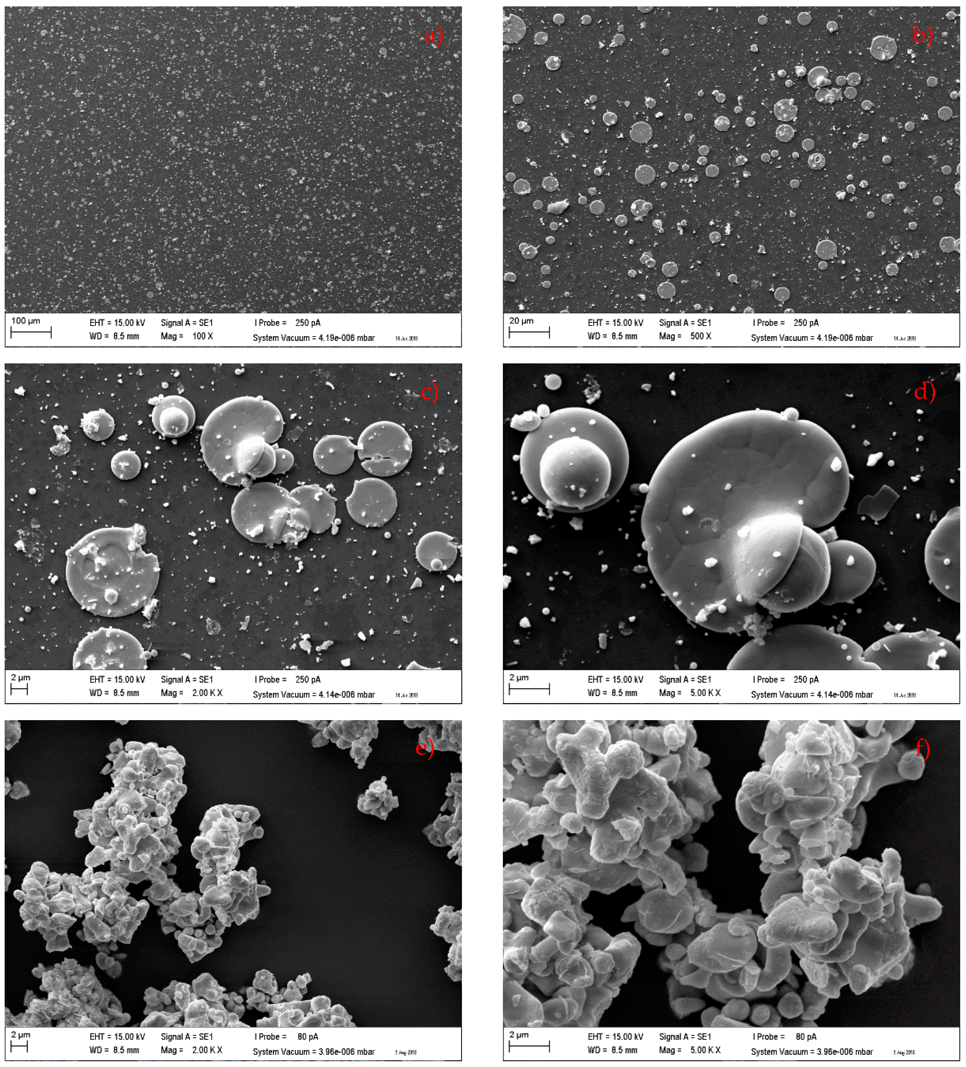
For the surface analysis, scanning electron microscopy (SEM) and laser scanning microscopy (LSM) measurements were performed. The SEM measurements were intended to give information about the structure produced by the atmospheric pressure plasma spraying process and are shown in Figure 1.
During the deposition process, the majority of the induced particles in the plasma torch were molten, resulting in circular droplets on the sample surface (compare powder reference Figure 1e,f to Figure 1a–d). The droplets were approx. 0.45 to 12 μm in diameter. The deposited particles did not produce a closed layer. The cover ratio was approx. 23%. In addition to the circular droplets, spheres were visible on the surface (Figure 1d).
The average thickness of the droplets was determined with LSM measurements at 0.24 ± 0.15 μm (N = 4). The following estimation could be made to verify the drop thickness. The grain size of the used bismuth oxide powder was <4 µm. Assuming that one powder grain can be considered as a sphere with a maximum radius of 2 µm, the results in a volume of 33.51 µm3 can be determined. The deposited droplets can be described as cylinders. The volume of the cylinder and the sphere can be considered as equal, neglecting decomposition processes and splash effects. Using the known volume of the cylinder and the measured diameter of one of the tallest droplets of the SEM images with r = 5.8 μm, the height can be calculated to 0.32 µm, which correlates to the measured thickness.
3.2. X-ray Diffraction (XRD)
The XRD patterns of the bismuth oxide droplets and the powder reference are shown in Figure 2. The powder reference showed two kinds of crystal structures: monoclinic (PDF-Nr.: 03-065-2366) and cubic (PDF-Nr.:01-071-0467) Bi2O3. The deposited droplets showed a mixed crystal structure of tetragonal nonstoichiometric Bi2O2.33 (PDF-Nr.: 00-027-0051) and monoclinic Bi2O3. The major reflex in the coating at 43.8° was assigned to the nonstoichiometric Bi2O2.33.
The cubic structure from the reference was not detected. The reflexes that could be verified from the monoclinic structure in the coating were at 32.6°, 41.25°, 42.25°, 50.1°, 50.39° and 71.64°. All others were not able to be detected. The tetragonal nonstoichiometric bismuth oxide phase could be generated, introducing oxygen into vacancies [24].
3.3. X-ray Photoelectron Spectroscopy (XPS)
XPS measurements were performed to determine the elemental composition and binding states for the bismuth powder reference and the coating. The samples contain three elements: bismuth, oxygen and carbon. In the deposited layer, silicon was also detected by the glass underground (Figure 3). All spectra were shifted to the adventitious carbon peak at 284.8 eV.
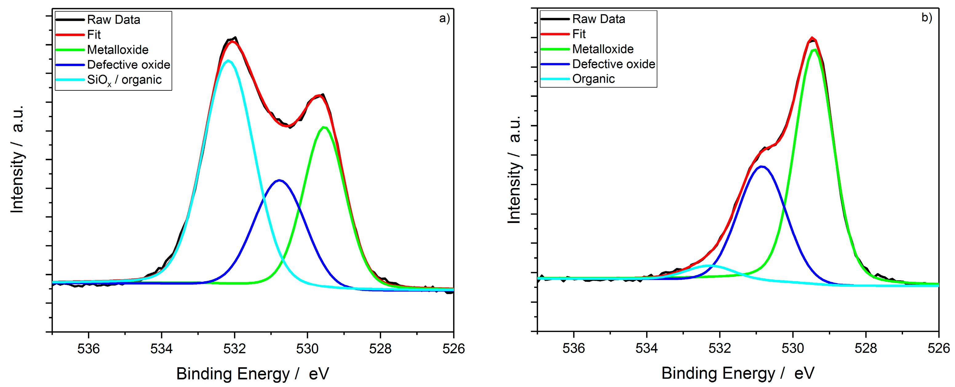
The O 1s peak shows the presence of three components and is pictured in Figure 4. The first structure corresponds to metallic oxygen (MO) at 529.5 eV with a FWHM of 1.3. The peak at 530.8 eV (FWHM 1.6) could be assigned to defective sites within the oxide crystal (DO) [29]. The peak at 532.2 eV was composed of organic compounds (org. C) (adventitious carbon [30]) and, in the case of the coating, silicon oxide [31] and organic compounds.
The atomic concentration of all elements with the split oxygen peak is shown in Table 1. To determine the ratio of oxygen to bismuth, the MO and DO proportion of the oxygen peak must be summed. The powder reference was in good agreement with the bismuth (III)-oxide. The tetragonal Bi2O2.33 found by the XRD in the layer could not be determined in the ratio of (MO + DO)/Bi 4f (1.46). There was a higher proportion of defects in the coating than in the powder reference.
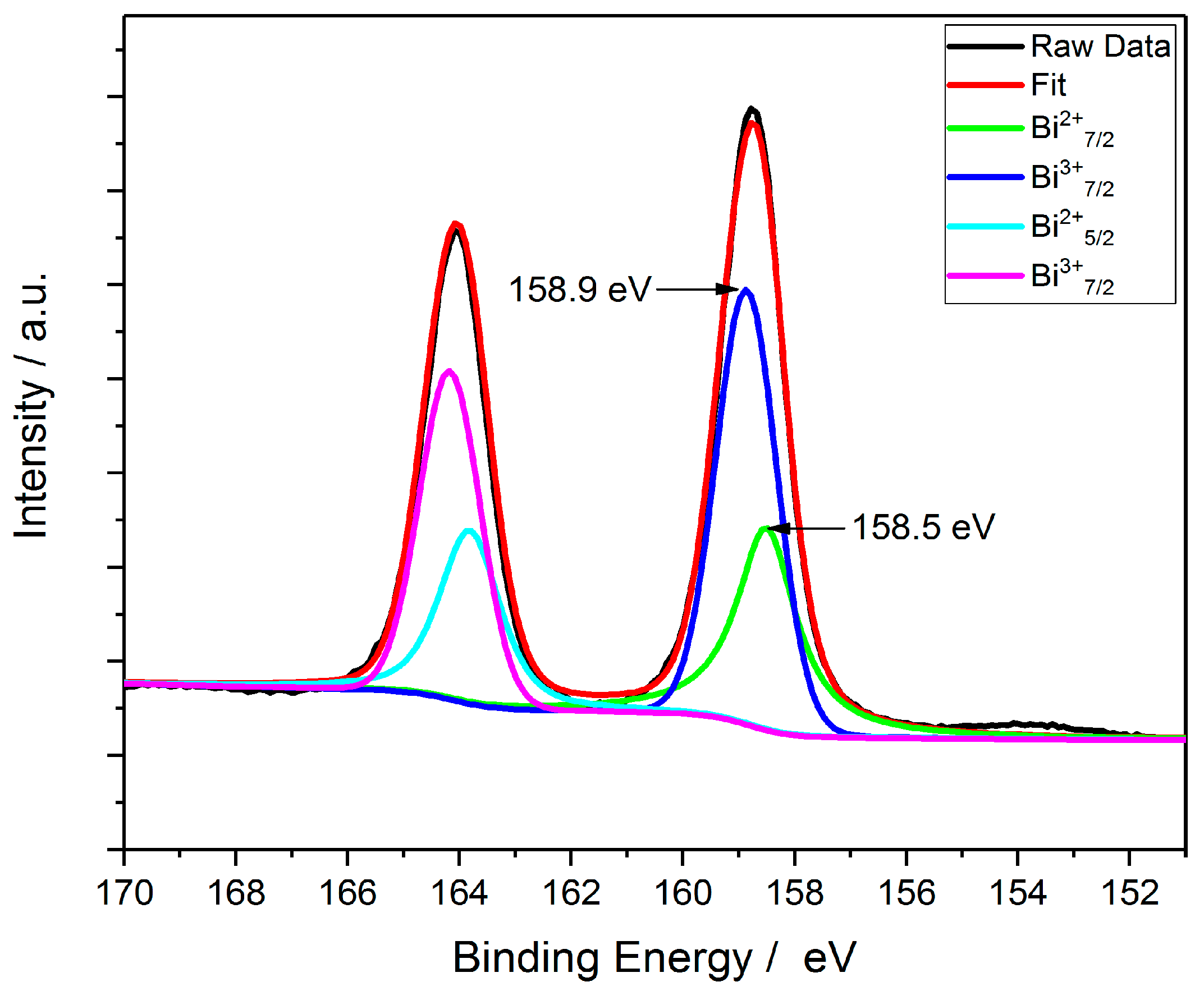
A direct shift in the Bi 4f7/2 peak between the reference and the coating with 158.6 and 158.7 eV was not apparent. Considering the assumption of the XRD data that Bi2O2.33 is represented in the coating, a split of Bi 4f into bismuth (II)-oxide and bismuth (III)-oxide could be adopted (Figure 5).
There are four main structures in the Bi 4f peak. The lower peak at 158.5 and 163.8 eV could be assigned to Bi2+ and the peak at 158.9 and 164.2 eV to Bi3+, which corresponds to Guan et al. [32]. This results in a proportion of 6.61 at.% and 9.98 at.% of Bi2+ and Bi3+.
3.4. Optical Characterization
Figure 6a shows the absorbance spectra of the coating. To determine the band gap from the absorbance, the Tauc-plot method was used, with the following equation [33,34]:
where Eg is the band gap, α the absorption coefficient, A is a constant, and hv is the photon energy. For the description of a direct or indirect band transition n = 1/2 or n = 2 [35]. The optical band gap can be determined via the extrapolation of the plots (αhv)2 or (αhv)1/2 vs. (hν), where α = 0 is set. This plot is shown in Figure 6b. Because no linear segment could be found in the plot (αhv)1/2 vs. (hν), it can be concluded that the deposited layer had a direct band gap [36] with Eg = 2.72 eV.
4. Conclusions
It has been shown that crystalline layers could be produced with the help of the plasma spraying process. The deposited layers had monoclinic Bi2O3 and tetragonal Bi2O2.33 crystal structures. Through the deposition process with the plasma jet, the amount of defective oxygen increased. The deposited layer had a direct band gap of Eg = 2.72 eV, which allowed its use as photocatalyst in the visible region of light.
Further investigations should validate the influence of plasma parameters (powder feed rate and speed, substrate transfer speed and input power) on layer thickness, chemical composition and crystal structure in the bandgap of resulting layers. Furthermore, a degradation test could be carried out with model pollutants.
Author Contributions
Conceptualization, R.K.; Methodology, R.K.; Validation, R.K., G.O., H.M., W.V.; Investigation, R.K.; Resources, G.O., H.M., W.V.; Writing-Original Draft Preparation, R.K.; Writing-Review & Editing, R.K., G.O., H.M., W.V.
Funding
This research was funded by Bundesministerium für Bildung und Forschung (03XP0015A/B).
Acknowledgments
The authors thank the German Research Foundation (DFG) for the provision of the XPS. We thank Helmut Klein from the department of Crystallography, Georg-August-University of Goettingen, for the support with the X-ray diffraction analysis.
Conflicts of Interest
The authors declare no conflict of interest.
References
- Iljinas, A.; Burinskas, S.; Dudonis, J. Synthesis of bismuth oxide thin films deposited by reactive magnetron sputtering. Acta Phys. Pol. A 2011, 120, 60–62. [Google Scholar] [CrossRef]
- Xia, J.-Y.; Tang, M.-T.; Cui, C.; Jin, S.-M.; Chen, Y.-M. Preparation of α-Bi2O3 from bismuth powders through low-temperature oxidation. Trans. Nonferrous Metals Soc. China 2012, 22, 2289–2294. [Google Scholar] [CrossRef]
- Tezel, F.M.; Kariper, İ.A. Synthesis, surface tension, optical and dielectric properties of bismuth oxide thin film. Mater. Sci. Pol. 2017, 35, 87–93. [Google Scholar] [CrossRef] [Green Version]
- Hou, J.; Yang, C.; Wang, Z.; Zhou, W.; Jiao, S.; Zhu, H. In situ synthesis of α-β phase heterojunction on Bi2O3 nanowires with exceptional visible-light photocatalytic performance. Appl. Catal. B Environ. 2013, 142–143, 504–511. [Google Scholar] [CrossRef]
- Shen, Y.D.; Li, Y.W.; Li, W.M.; Zhang, J.Z.; Hu, Z.G.; Chu, J.H. Growth of Bi2O3 ultrathin films by atomic layer deposition. J. Phys. Chem. C 2012, 116, 3449–3456. [Google Scholar] [CrossRef]
- Shimanoe, K. Bismuth oxide thin film as new electrochromic material. Solid State Ion. 1998, 113–115, 415–419. [Google Scholar] [CrossRef]
- Gujar, T.P.; Shinde, V.R.; Lokhande, C.D.; Mane, R.S.; Han, S.-H. Bismuth oxide thin films prepared by chemical bath deposition (CBD) method: Annealing effect. Appl. Surf. Sci. 2005, 250, 161–167. [Google Scholar] [CrossRef]
- Cornei, N.; Tancret, N.; Abraham, F.; Mentré, O. New ε-Bi2O3 metastable polymorph. Inorg. Chem. 2006, 45, 4886–4888. [Google Scholar] [CrossRef] [PubMed]
- Deng, H.Y.; Xu, H.Z.; Hao, W.C. A Transition phase in the transformation from α-, β- and ε- to δ-bismuth oxide. Chin. Phys. Lett. 2011, 28, 056101. [Google Scholar] [CrossRef]
- Gualtieri, A.F.; Immovilli, S.; Prudenziati, M. Powder X-ray diffraction data for the new polymorphic compound ω-Bi2O3. Powder Diffr. 1997, 12, 90–92. [Google Scholar] [CrossRef]
- Harwig, H.A.; Gerards, A.G. The polymorphism of bismuth sesquioxide. Thermochim. Acta 1979, 28, 121–131. [Google Scholar] [CrossRef]
- Mehring, M. From molecules to bismuth oxide-based materials: Potential homo- and heterometallic precursors and model compounds. Coord. Chem. Rev. 2007, 251, 974–1006. [Google Scholar] [CrossRef]
- Klinkova, L.A.; Nikolaichik, V.I.; Barkovskii, N.V.; Fedotov, V.K. Thermal stability of Bi2O3. Russ. J. Inorg. Chem. 2007, 52, 1822–1829. [Google Scholar] [CrossRef]
- Patil, R.B.; Puri, R.K.; Puri, V. Intrinsic stress of bismuth oxide thin films: Effect of vapour chopping and air ageing. J. Phys. Conf. Ser. 2008, 114, 012036. [Google Scholar] [CrossRef]
- Kumari, L.; Lin, J.-H.; Ma, Y.-R. Synthesis of bismuth oxide nanostructures by an oxidative metal vapour phase deposition technique. Nanotechnology 2007, 18, 295605. [Google Scholar] [CrossRef]
- Takeyama, T.; Takahashi, N.; Nakamura, T.; Itoh, S. Microstructure characterization of δ-Bi2O3 thin film under atmospheric pressure by means of halide CVD on c-sapphire. J. Cryst. Grow. 2005, 275, 460–466. [Google Scholar] [CrossRef]
- Yang, X.; Lian, X.; Liu, S.; Wang, G.; Jiang, C.; Tian, J.; Chen, J.; Wang, R. Enhanced photocatalytic performance: A β-Bi2O3 thin film by nanoporous surface. J. Phys. D Appl. Phys. 2013, 46, 035103. [Google Scholar] [CrossRef]
- Ratova, M.; Marcelino, R.B.P.; de Souza, P.P.; Amorim, C.C.; Kelly, P.J. Reactive Magnetron Sputter Deposition of Bismuth Tungstate Coatings for Water Treatment Applications under Natural Sunlight. Catalysts 2017, 7, 283. [Google Scholar] [CrossRef]
- Sabaghiana, M.; Behzada, M.; Jahromib, H.S. Alfa-bismuth(III) oxide catalyzed biginelli reactions using experimentally designed optimized condition. J. Adv. Mater. Process. 2015, 3, 61–69. [Google Scholar]
- Condurache-Bota, S.; Constantinescu, C.; Praisler, M.; Tiron, V.; Tigau, N.; Gheorghies, C. The influence of laser wavelength and pulses number on the structure and the optical properties of pulsed laser-deposited bismuth oxide thin films. In Proceedings of the 2014 International Semiconductor Conference (CAS), Sinaia, Romania, 13–15 October 2014; pp. 87–90. [Google Scholar]
- Condurache-Bota, S.; Rusu, G.I.; Tigau, N.; Drasovean, R.; Gheorghies, C. Structural and optical characterization of thermally oxidized bismuth films. Rom. J. Chem. 2009, 54, 205–211. [Google Scholar]
- Killedar, V.V.; Bhosale, C.H.; Lokhande, C.D. Characterization of spray deposited bismuth oxide thin films from non-aqueous medium. Turk. J. Phys. 1998, 22, 825–830. [Google Scholar]
- Wang, X.; Zhu, A.; Li, Z.; Liu, Z. Ag doped Bi2O2.33 microrods: Photocatalytic activity investigation. RSC Adv. 2016, 6, 25409–25415. [Google Scholar] [CrossRef]
- Salim, E.T.; Al-Douri, Y.; Al Wazny, M.S.; Fakhri, M.A. Optical properties of Cauliflower-like Bi2O3 nanostructures by reactive pulsed laser deposition (PLD) technique. Sol. Energy 2014, 107, 523–529. [Google Scholar] [CrossRef]
- Fang, G.; Chen, G.; Liu, J.; Wang, X. Ultraviolet-Emitting Bi2O2.33 Nanosheets Prepared by Electrolytic Corrosion of Metal Bi. J. Phys. Chem. C 2009, 114, 864–867. [Google Scholar] [CrossRef]
- Schuisky, M.; Hårsta, A. Epitaxial growth of Bi2O2.33 by halide CVD. Chem. Vap. Depos. 1996, 2, 235–238. [Google Scholar] [CrossRef]
- Huang, X.; Yan, J.; Zeng, F.; Yuan, X.; Zou, W.; Yuan, D. Facile preparation of orange-like Bi2O2.33 microspheres for high performance supercapacitor application. Mater. Lett. 2013, 90, 90–92. [Google Scholar] [CrossRef]
- Köhler, R.; Sauerbier, P.; Militz, H.; Viöl, W. Atmospheric pressure plasma coating of wood and MDF with polyester powder. Coatings 2017, 7, 171. [Google Scholar] [CrossRef]
- Biesinger, M.C.; Payne, B.P.; Lau, L.W.M.; Gerson, A.; St. Smart, R.C. X-ray photoelectron spectroscopic chemical state quantification of mixed nickel metal, oxide and hydroxide systems. Surf. Interface Anal. 2009, 41, 324–332. [Google Scholar] [CrossRef] [Green Version]
- Barr, T.L.; Seal, S. Nature of the use of adventitious carbon as a binding energy standard. J. Vac. Sci. Technol. A Vac. Surf. Films 1995, 13, 1239–1246. [Google Scholar] [CrossRef]
- Beamson, G.; Briggs, D. High Resolution XPS of Organic Polymers: The Scienta ESCA300 Database; Wiley: New York, NY, USA; Chichester, UK, 1992. [Google Scholar]
- Guan, H.; Zhang, X.; Xie, Y. Soft-chemical synthetic nonstoichiometric Bi2O2.33 nanoflower: A new room-temperature ferromagnetic semiconductor. J. Phys. Chem. C 2014, 118, 27170–27174. [Google Scholar] [CrossRef]
- Gondal, M.A.; Saleh, T.A.; Drmosh, Q. Optical properties of bismuth oxide nanoparticles synthesized by pulsed laser ablation in liquids. Sci. Adv. Mater. 2012, 4, 507–510. [Google Scholar] [CrossRef]
- Sirota, B.; Reyes-Cuellar, J.; Kohli, P.; Wang, L.; McCarroll, M.E.; Aouadi, S.M. Bismuth oxide photocatalytic nanostructures produced by magnetron sputtering deposition. Thin Solid Films 2012, 520, 6118–6123. [Google Scholar] [CrossRef]
- Leontie, L.; Caraman, M.; Visinoiu, A.; Rusu, G.I. On the optical properties of bismuth oxide thin films prepared by pulsed laser deposition. Thin Solid Films 2005, 473, 230–235. [Google Scholar] [CrossRef]
- Enhessari, M.; Shaterian, M.; Esfahani, M.J.; Motaharian, M.N. Synthesis, characterization and optical band gap of La2CuO4 nanoparticles. Mater. Sci. Semicond. Process. 2013, 16, 1517–1520. [Google Scholar] [CrossRef]
Figure 1.
SEM images of coated borosilicate glass with different magnification (a) 100×, (b) 500×, (c) 2000×, and (d) 5000×; Powder reference with different magnification (e) 2000× and (f) 5000×.
Figure 1.
SEM images of coated borosilicate glass with different magnification (a) 100×, (b) 500×, (c) 2000×, and (d) 5000×; Powder reference with different magnification (e) 2000× and (f) 5000×.

Figure 2.
XRD plot of coating and powder reference, with ▪ monoclinic Bi2O3, + cubic Bi2O3 and # tetragonal Bi2O2.33.
Figure 2.
XRD plot of coating and powder reference, with ▪ monoclinic Bi2O3, + cubic Bi2O3 and # tetragonal Bi2O2.33.
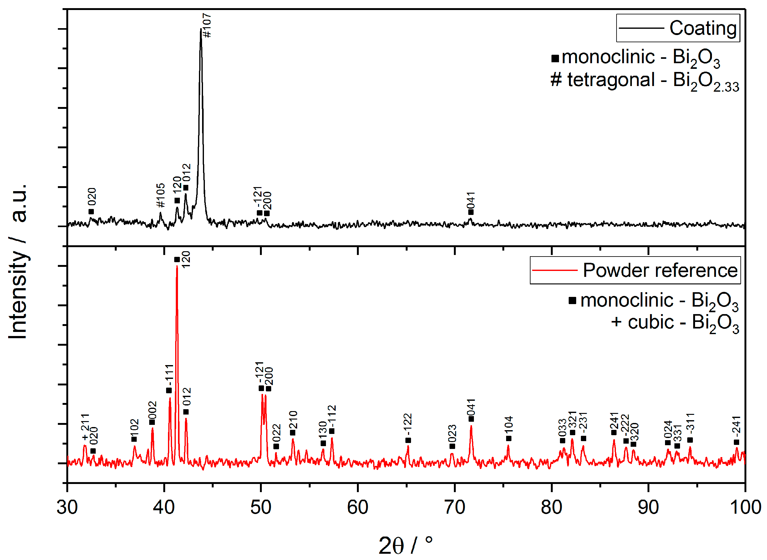
Figure 3.
XPS-survey spectra of coating and powder reference (a); Detail spectra of coating (b) O 1s, (c) Bi 4f, (d) C 1s (e) Si 2p.
Figure 3.
XPS-survey spectra of coating and powder reference (a); Detail spectra of coating (b) O 1s, (c) Bi 4f, (d) C 1s (e) Si 2p.
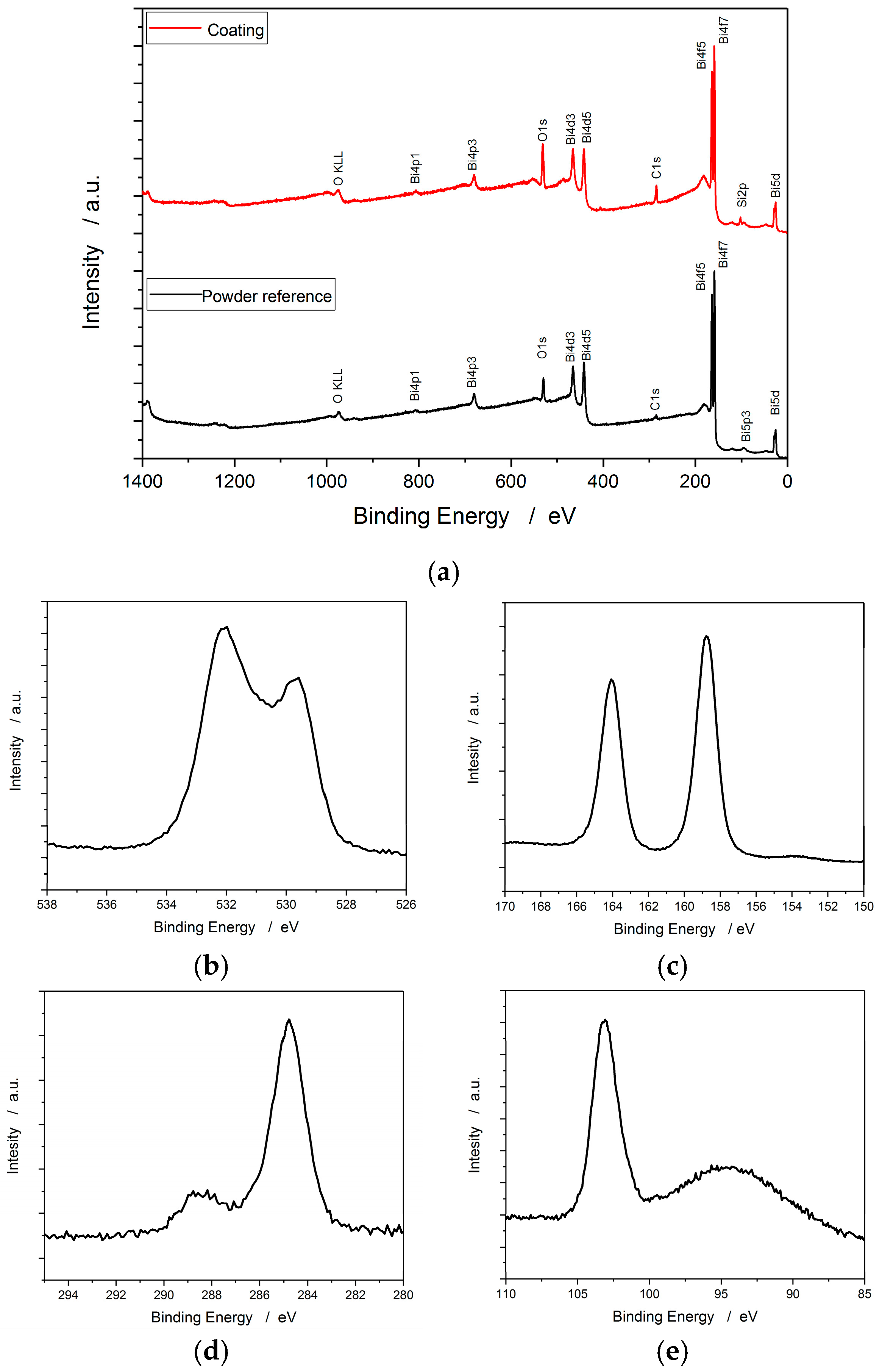
Figure 4.
O 1s detail spectra of deposit layer (a) and powder reference (b).

Figure 5.
Bi 4f detail spectra of the coating with splitting in Bi2+ and Bi3+.

Figure 6.
(a) UV-Vis absorbance spectra of plasma-coated bismuth oxide borosilicate glass; (b) Plot of (αhν)2 vs. (hν) to determine the direct band gap; N = 4.
Figure 6.
(a) UV-Vis absorbance spectra of plasma-coated bismuth oxide borosilicate glass; (b) Plot of (αhν)2 vs. (hν) to determine the direct band gap; N = 4.


Table 1.
Atomic concentration of the powder reference and the coating in at.% with a split oxygen peak and the ratio of metal oxide/bismuth, sum of metal oxide and defective oxide/bismuth and defective oxide/bismuth.
Table 1.
Atomic concentration of the powder reference and the coating in at.% with a split oxygen peak and the ratio of metal oxide/bismuth, sum of metal oxide and defective oxide/bismuth and defective oxide/bismuth.
| Sample | C 1s | MO | DO | org. C | SiOx and org. C |
| Powder reference | 18.3 | 30.86 | 16.55 | 2.16 | – |
| Coating | 24.95 | 13.97 | 10.32 | – | 23.12 |
| Sample | Si 2p | Bi 4f | Ratio of MO/Bi 4f | Ratio of MO + DO/Bi 4f | Ratio of DO/Bi 4f |
| Powder reference | – | 32.13 | 0.96 | 1.48 | 0.52 |
| Coating | 11.05 | 16.59 | 0.84 | 1.46 | 0.62 |
© 2018 by the authors. Licensee MDPI, Basel, Switzerland. This article is an open access article distributed under the terms and conditions of the Creative Commons Attribution (CC BY) license (http://creativecommons.org/licenses/by/4.0/).
Share and Cite
MDPI and ACS Style
Köhler, R.; Ohms, G.; Militz, H.; Viöl, W. Atmospheric Pressure Plasma Coating of Bismuth Oxide Circular Droplets. Coatings 2018, 8, 312. https://doi.org/10.3390/coatings8090312
AMA Style
Köhler R, Ohms G, Militz H, Viöl W. Atmospheric Pressure Plasma Coating of Bismuth Oxide Circular Droplets. Coatings. 2018; 8(9):312. https://doi.org/10.3390/coatings8090312
Chicago/Turabian StyleKöhler, Robert, Gisela Ohms, Holger Militz, and Wolfgang Viöl. 2018. "Atmospheric Pressure Plasma Coating of Bismuth Oxide Circular Droplets" Coatings 8, no. 9: 312. https://doi.org/10.3390/coatings8090312
Note that from the first issue of 2016, this journal uses article numbers instead of page numbers. See further details here.