Influence of Ge Incorporation from GeSe2 Vapor on the Properties of Cu2ZnSn(S,Se)4 Material and Solar Cells

1
Institute of Photovoltaics, Nanchang University, Nanchang 330031, China
2
College of Physics Science and Technology, Hebei University, Baoding 071002, China
*
Author to whom correspondence should be addressed.
Coatings 2018, 8(9), 304; https://doi.org/10.3390/coatings8090304
Submission received: 18 July 2018
/
Revised: 15 August 2018
/
Accepted: 24 August 2018
/
Published: 28 August 2018
(This article belongs to the Special Issue Thin Films for Energy Harvesting, Conversion, and Storage)
Abstract
:Cu2ZnSn(S,Se)4 (CZTSSe) and Cu2Zn(Sn,Ge)(S,Se)4 (CZTGSSe) thin films were prepared based on a non-vacuum solution method. The CZTSSe films were obtained by annealing the solution-deposited precursor films with Se, while the CZTGSSe films were obtained by annealing the similar precursor films with Se and GeSe2. We found that Ge could be incorporated into the annealed films when GeSe2 was present during the annealing process. The Ge incorporation obviously enlarged the sizes of the crystalline grains in the annealed films. However, the energy dispersive spectrometry (EDS) measurements revealed that the element distribution was not uniform in the CZTGSSe films. We fabricated solar cells based on the CZTSSe and CZTGSSe films. It was found the Ge incorporation decreases the Eu energy of the absorber material. The solar cell efficiency was increased from 5.61% (CZTSSe solar cell) to 7.14% (CZTGSSe solar cell) by the Ge incorporation. Compared to CZTSSe solar cells, the CZTGSSe solar cells exhibited a lower diode ideality factor and lower reverse saturation current density.
1. Introduction
The Cu2ZnSn(S,Se)4 (CZTSSe) material has gained a great deal of attention as a promising photovoltaic material due to its properties, including suitable optical bandgap (1.0–1.5 eV), high absorption coefficient (>10−4 cm−1 in the visible light region), and Earth-abundant nature [1]. To-date, the efficiencies of CZTSSe solar cells have increased to 12.6% [2]. However, this efficiency is much lower than the efficiencies of mature Cu(In,Ga)Se2 (CIGS) or CdTe solar cells. The efficiencies of CZTSSe solar cells are mainly limited by the low open-circuit voltage, which could be related with the poor properties (e.g., unfavorable electrical defects, secondary phases, large band-tail energy) of the CZTSSe material [3].
Recently, Giraldo et al. found that the properties of CZTSSe material can be greatly improved by Ge incorporation [4,5,6]. The Ge incorporation in CZTSSe material can increase the sizes of the crystalline grains, increase the carrier lifetime, decrease the band-tail energy, prevent the formation of deep-level defects, and more [4]. Moreover, the GeO formed in the grain-boundaries was believed to passivate the grain boundaries [5]. Several groups have incorporated Ge into CZTSSe, and they found the Ge incorporation can indeed increase the open-circuit voltage and efficiency of the solar cell [6,7]. For most of the Ge-incorporated CZTSSe materials produced by the two-step method, the Ge element was introduced during the precursor preparation. The Ge may also be introduced into the material during the annealing process. For example, Umehara et al. reported on the preparation of Cu2SnxGe1−xS3 material by annealing co-sputtered Cu-Sn films with S and GeS2 vapor [8].
In this paper, we prepared CZTSSe and Ge-incorporated Cu2Zn(Sn,Ge)(S,Se)4 (CZTGSSe) thin films based on a non-vacuum solution method. The Ge incorporation was realized by annealing the solution-deposited precursor films with Se and GeSe2, while the CZTSSe films were prepared by annealing precursor films with only Se. By comparing the morphologies, compositions, and crystallinities of the CZTSSe and CZTGSSe films, we investigated the influence of the Ge incorporation by this method on the properties of CZTSSe material. Based on the prepared CZTSSe and CZTGSSe films, solar cells were fabricated and their performances were compared.
2. Materials and Methods
Mo-coated soda-lime glass (Mo/SLG) was used as substrate for the preparation of the films. After the cleaning of the substrates, precursor films were prepared on the substrates by spin-coating the precursor solution, which was prepared by successively dissolving copper(II)-acetate monohydrate (99.99%, 2.3 mmol), tin(II)-chloride dehydrate (99.99%, 1.6 mmol), zinc(II)-chloride (99.99%, 1.6 mmol), and thiourea (99.5%, 5.5 mmol) into 2 mL of dimethyl sulfoxide (99.9%). For the spin-coating process, 200 μL of the precursor solution was first dipped on the substrate, then the substrate was spun at 500 r/min for 30 s and 2000 r/min for 120 s successively. After the spin-coating process, the films were dried at 300 °C for 2 min. These processes were repeated several times until the film thickness reached approximately 1 μm. Both the spin-coating process and the drying process were carried out in a glove box filled with nitrogen.
After the preparation of precursor films, they were annealed in a furnace to prepare the CZTSSe or CZTGSSe films. For the preparation of CZTGSSe films, the precursor films with Se pellets and GeSe2 powder were first placed in a graphite box. The graphite box was then transferred into a tube furnace. After that, the tube was evacuated and refilled with nitrogen to a pressure of 100 Torr. Finally, the furnace was heated to 600 °C for 15 min. The preparation of CZTSSe films was the same as with CZTGSSe films, except no GeSe2 was used during the annealing process.
Solar cells based on the CZTSSe or CZTGSSe films were fabricated using the following structure: Mo/CZT(G)SSe/CdS/i-ZnO/AZO (Al-doped ZnO)/Ag (i-ZnO is short for intrinsic ZnO). A mixed solution of 3 mM cadmium acetate, 0.25 M thiourea, and 1 M ammonia hydroxide was used for the buffer deposition. The CdS buffer layer was deposited by placing the substrate into the deposition solution with a temperature of 75 °C. After 10 min deposition, a CdS buffer layer with a thickness of ~50 nm was deposited on the absorber layer. Then, an i-ZnO layer with a thickness of ~50 nm and an AZO (Al-doped ZnO) layer with a thickness of ~200 nm was successively deposited on the buffer layer by sputtering. The pressure of the Ar gas during the sputtering was 0.3 Pa, and the sputtering powers were 50 W and 100 W for i-ZnO and AZO, respectively. Ag grids were deposited on the AZO layer using a thermal evaporation setup, and the thickness of the Ag grid was approximately 200 nm. Finally, the prepared solar cell was divided into small individual solar cells with area ~1 cm2.
The constitutions of the films were analyzed by a Bruker D8 Advance X-ray diffractometer (Billerica, MA, USA) and a JY LabRAM HR Raman spectrometer (Horiba, Kyoto, Japan) equipped with a 532 nm laser. The surface morphologies of the films were characterized by a FEI JSM-7500F scanning electron microscope (SEM) (JEOL, Ltd., Tokyo, Japan). The compositions of the thin films were analyzed by an energy dispersive spectrometer (EDS) that was attached in the SEM setup. The solar cell performances were characterized by an Agilent B1500A semiconductor parametric analyzer (Agilent Technologies, Santa Clara, CA, USA) under AM 1.5 global solar irradiations. The quantum efficiency (QE) curves of the solar cells were measured by a QTesT 1000ADX setup (Crowntech, Macungie, PA, USA).
3. Results and Discussion
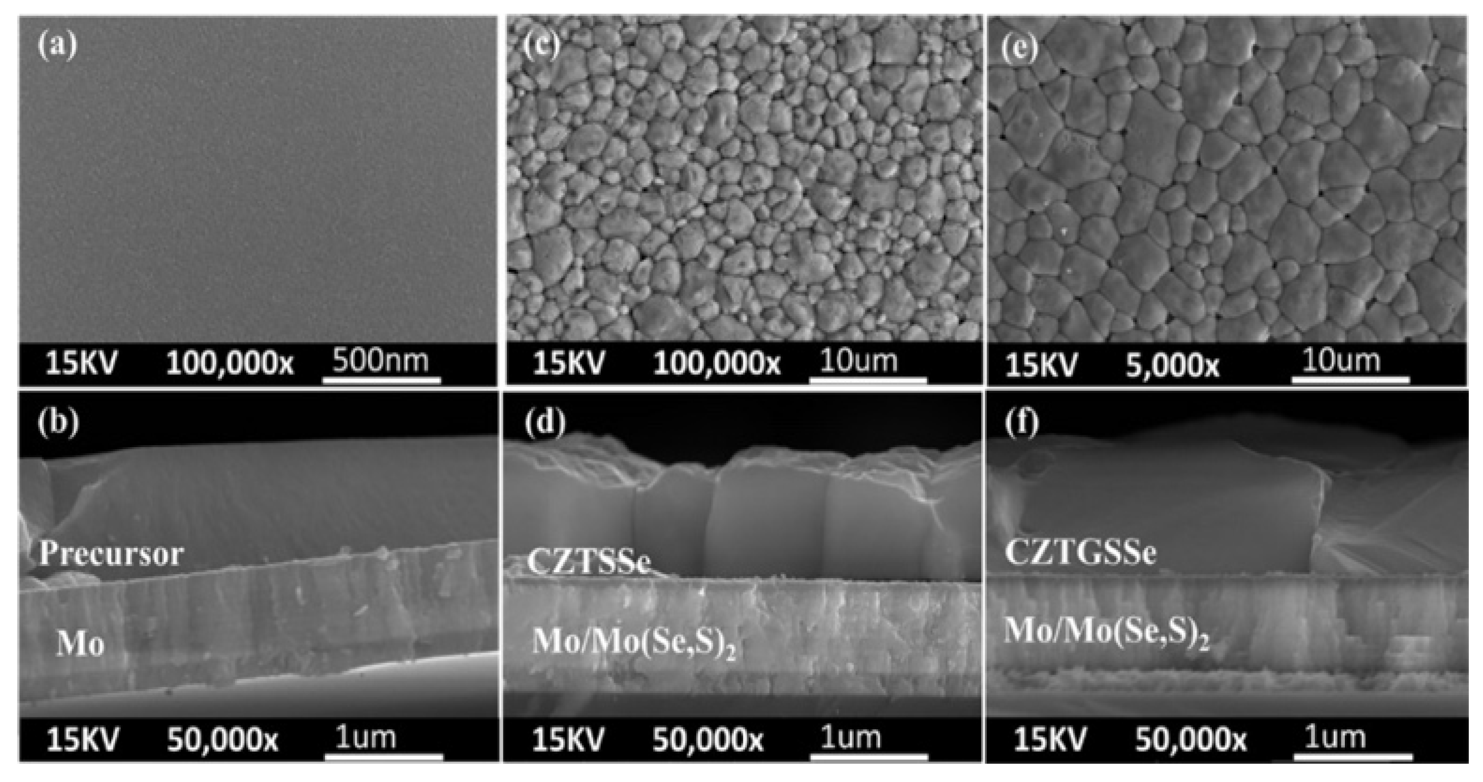
Figure 1 shows the typical SEM images of the precursor film and the films after different annealing processes. The precursor film looked smooth on the surface, and no obvious crystalline grains were found in the film (Figure 1a,b). After annealing with Se, crystalline grains with sizes 1–4 μm could be seen in the film (Figure 1c,d). The film showed dense morphology, but the surface became coarse. When GeSe2 was added during the annealing process, the sizes of the crystalline grains in the annealed film became greater than those in the film annealed with only Se.
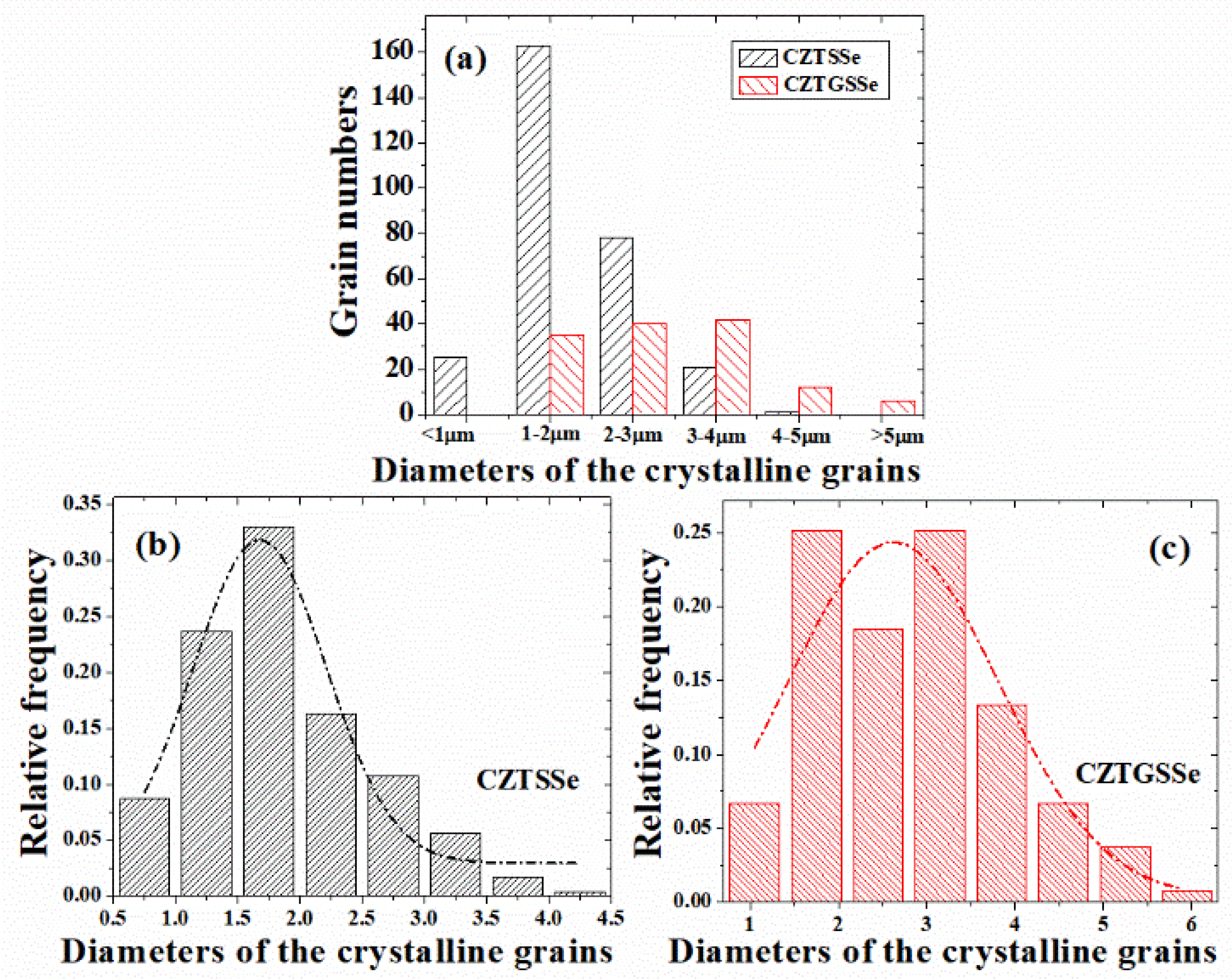
We counted the crystalline grains in the annealed films and measured their sizes. Based on our counting, the average sizes of the crystalline grains in CZTSSe and CZTGSSe films were 1.86 μm and 2.84 μm. Therefore, the use of GeSe2 during the annealing process enlarged the grain sizes by 53%. We also counted the distribution of the grain sizes in CZTSSe and CZTGSSe films. The statistics were fitted using Gauss curves (Figure 2b,c). The peak positions of the fitting curves for CZTSSe and CZTGSSe films were at 1.67 μm and 2.62 μm, respectively. These values were close to the average grain sizes in CZTSSe and CZTGSSe films.
Table 1 shows the compositions of the precursor film and the films after different annealing processes. It should be noted that our XRD measurement (shown below) conformed with the formation of Mo(S,Se)2 between the substrate and the annealed films, as Mo(S,Se)2 contains S and Se, and the Mo and S peaks coincided in the EDS spectrum. The presence of Mo(S,Se)2 may have influenced the EDS measurement in the CZTSSe or CZTGSSe films, and the atomic percent of S and Se may slightly deviate from the real values in the films. However, the ratios between the metal elements were not influenced by the formation of Mo(S,Se)2. The Cu/(Zn + Sn) and Zn/Sn ratios in the precursor film were similar to that in the precursor solution. After annealing with Se, both the Cu/(Zn + Sn) and Zn/Sn ratios in the film increased, which could be caused by the Sn loss during the annealing process. The composition of the film that annealed with Se was close to the optimum composition (Cu/(Zn + Sn) = 0.8, Zn/Sn = 1.2) for Cu2ZnSnS4-based photovoltaic material [9]. When GeSe2 was used for the annealing, Ge was found to be present in the annealed film (Ge/(Sn + Ge) = 0.37). Due to the incorporation of Ge, both the ratio of Cu/(Zn + Sn + Ge) and Zn/(Sn + Ge) in the film decreased, and thus the composition of the films slightly deviated from the optimum composition for CZTSSe-based material.
The EDS results proved that Ge was incorporated into the films that were selenized with Se and GeSe2. As the precursor films contained no Ge, the Ge element in the annealed film must have come from the GeSe2 powder which was placed into the graphite box before the selenization. However, the GeSe2 powder did not directly contact the films during the annealing. Therefore, the mechanism by which the Ge element transferred from the GeSe2 powder to the annealed film could be interesting. To determine this mechanism, we checked the properties of GeSe2 and found that GeSe2 can vaporize at around 600 °C [10]. Therefore, we believe that GeSe2 vapor could be present in the graphite box during the annealing process, which would result in the diffusion of Ge from the surface to the bulk of the films. As discussed in [6], the incorporated Ge may react with Se to form a specific liquid phase. The liquid phase can assist in the diffusion of the elements and the crystallization of the material, so the films selenized with Se and GeSe2 showed larger crystalline grains.
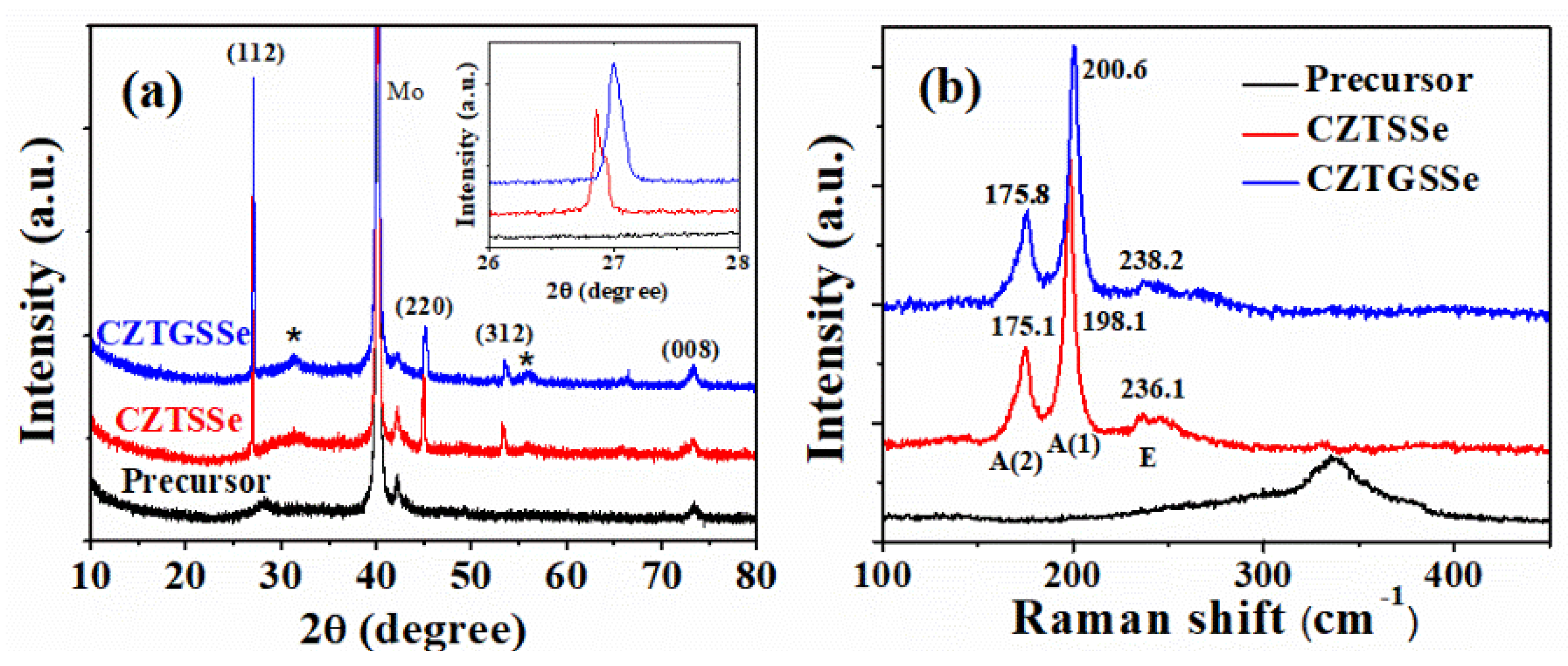
Figure 3 shows the XRD patterns and Raman spectra of the precursor and annealed films. The results proved that the main phase in the annealed film was CZTSSe or CZTGSSe (XRD peaks at around 27°, 45°, 53° and Raman peaks at around 175, 198, and 235 cm−1 could be attributed to CZTSSe or CZTGSSe) [9,11]. However, a small amount of secondary phases such as Zn(S,Se) and CuxSe (Raman peak at around 250 cm−1, and 265 cm−1, respectively) may exist in the films [9]. Besides, Mo(S,Se)2 (XRD peak at around 32° and 56°) was formed between CZTSSe/CZTGSSe and Mo contact. Compared to the CZTSSe film, the XRD and Raman peak of CZTGSSe film shifted to a high angle or high wavenumber (shift from 26.9° to 27.0° for (112) diffraction peak, and from 198.1 cm−1 to 200.6 cm−1 for the main Raman peak), which agrees with previous reports [11,12,13]. The reason for this phenomenon could be that the Ge incorporation changes the lattice parameters and modifies the phonon mode of the material. Based on the XRD data, we calculated the lattice parameters of CZTSSe and CZTGSSe materials (a = 5.71 Å, c = 11.63 Å for CZTSSe; a = 5.69 Å, c = 11.48 Å for CZTGSSe). These values are in coincide with the published results [11,12,13].
Surprisingly, we found that the XRD and Raman peaks of the film were broadened when GeSe2 was used for the annealing. For the CZTSSe film, the full width at half maxima (FWHM) of the (112) diffraction peak and the main Raman peak were 0.10° and 5.4 cm−1, respectively. For the CZTGSSe film, the FWHM of the (112) peak and the main Raman peak were 0.13° and 6.1 cm−1, respectively. This result seems to contradict the fact that the usage of GeSe2 greatly improved the size of the crystalline grains in the film. We checked the literature and found that similar behavior of Ge incorporation has been reported. In Reference [14], the authors found the Ge incorporation broadened the XRD peaks and attributed this to the non-uniform distribution of the Ge element in the material (i.e., some of the region may be Ge-rich but other regions may be Ge-poor). So, we carried out EDS mapping measurement on the Ge-incorporated film, and the results are shown in Figure 4. From the figure, we see the that the distributions of Cu, Zn, and Sn were relatively uniform, but S and Se were not uniformly distributed, which is similar to the report in Reference [15]. Besides, the distribution of Ge was also not uniform. In some of the regions, Ge was rich at the grain boundaries. In other regions, however, Ge was rich inside the crystalline grains. Therefore, the lattice parameters of the material in different regions would be different due to different compositions. Since the XRD pattern of the whole film is the combination of the XRD patterns from different regions of the film, the inhomogeneous distribution of the elements may result in the enlarged FWHM in XRD and Raman results.
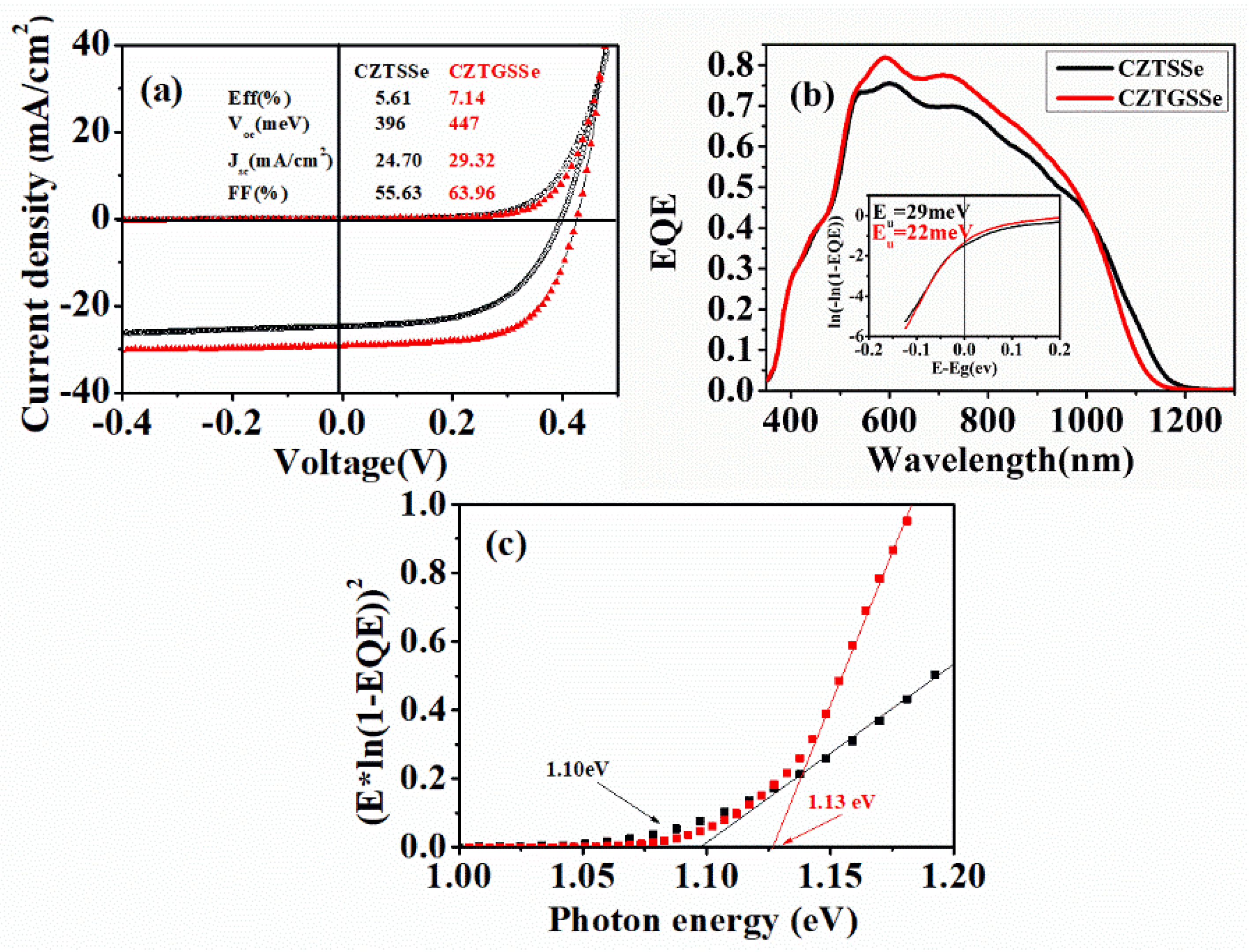
We fabricated solar cells based on the CZTSSe and CZTGSSe films. Figure 5 shows the J–V and QE results of the fabricated solar cells. Compared to the CZTSSe solar cell, the CZTGSSe solar cell showed better performances, even though the distribution of Ge in the CZTGSSe material was inhomogeneous and the composition of CZTGSSe was not optimal. The open-circuit voltage, short-circuit current density, and fill factor for the CZTGSSe solar cell were all larger than the parameters for the CZTSSe solar cell. Therefore, the efficiency of the solar cell was improved from 5.61% to 7.14% by Ge incorporation. QE measurements revealed that the CZTGSSe solar cell could respond better than the CZTSSe solar cell in the wavelength region of 500–1000 nm. This means less recombination of the photo-carriers was achieved in the bulk of the CZTGSSe absorber layer, so more photo-carriers could be collected for the CZTGSSe solar cell [16]. We estimated the band-gap energies of the absorber materials based on the EQE (external quantum efficiency) data (Figure 5c), which were 1.10 eV for CZTSSe and 1.13 eV for CZTGSSe. A larger band-gap energy means less absorption of the light with long wavelength, and therefore the EQE of CZTGSSe solar cell was lower than the QE of the CZTSSe solar cell in the wavelength region above 1000 nm. Moreover, we calculated the Eu energies of the absorber materials based on the EQE data in the long wavelength region, which were 29 meV for the CZTSSe absorber and 22 meV for the CZTGSSe absorber. For materials with low crystallinity or disordered structure, there were large amounts of localized states which could be extended in the band gap. This could cause the exponential part (Urbach tail) near the optical band gap in the absorption coefficient curve. Urbach energy (Eu) is often interpreted as the width of the Urbach tail. A large Eu energy normally means the material has poor crystallinity or disordered micro-structures. A [CuZn + ZnCu] disorder often exists in Cu2ZnSnS4-based materials, which is believed to be an important factor limiting the performance of the solar cells [17]. The calculated Eu energies of CZTSSe and CZTGSSe indicated that the Ge incorporation could alleviate the formation of localized states in the material, which is beneficial to the solar cells. The results above prove that the Ge incorporation by our method is a promising way to improve the quality of solar cell absorber material. By further optimizing the preparation process of this method, we believe that high-quality CZTGSSe material with optimized composition and uniform Ge distribution could be obtained.
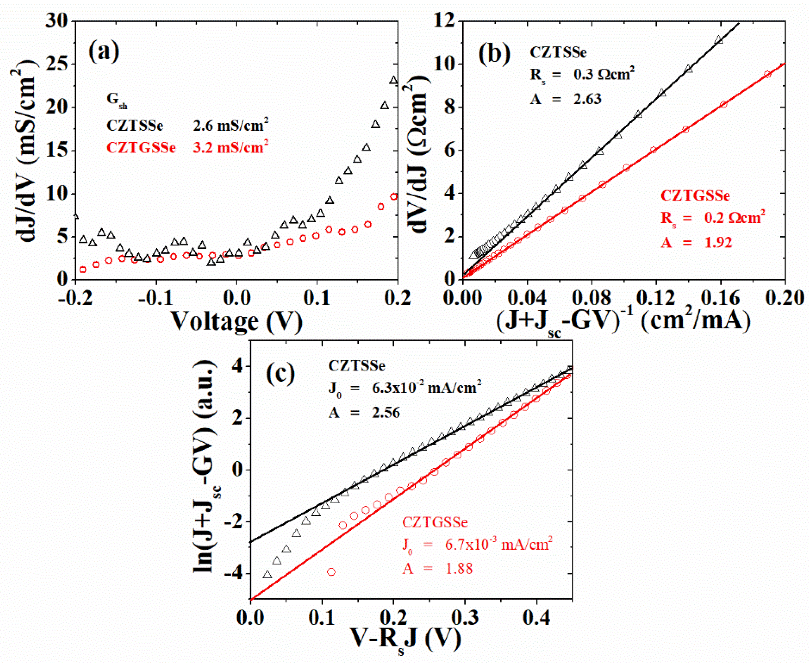
To further analyze the electrical properties of the solar cells, we estimated the shunt resistance (Rsh), series resistance (Rs), diode ideality factor (A), and reverse saturation current density (J0) of the solar cells based on the J–V data [16]. Figure 6a shows the estimation of Gsh (Gsh = 1/Rsh). The Gsh of the CZTGSSe solar cell was higher than that of the CZTSSe cell, which may be related to the inhomogeneous distribution of the elements—especially in the grain boundaries (therefore, a small shunt path may exist in the grain boundaries). The estimation in Figure 6b,c gives similar values of ideality factor (2.63 and 2.56 for the CZTSSe solar cell, 1.92 and 1.88 for the CZTGSSe solar cell). The value of the ideality factor can give information about the dominant recombination mechanism in the solar cell. According to [18], an ideality factor lower than but close to 2 means that the main recombination mechanism in the solar cell is the recombination in the space charge region via deep defect levels, while an ideality factor larger than 2 indicates that the main recombination mechanism in the solar cell is the tunnel-enhanced recombination in the space charge region (the tunnel effect can happen for materials with a high concentration of localized states). Therefore, the incorporation of Ge in the absorber layer modifies the main recombination mechanism of the solar cells. This indicates that the Ge incorporation may modify the defect formations in the absorber material, as recombination is closed related with the electrical defects in the material. Figure 6c shows that the J0 values were 6.3 × 10⁻² mA/cm2 and 6.7 × 10⁻³ mA/cm2 for CZTSSe and CZTGSSe solar cells, respectively. The J0 was dominated by the recombination of the carriers in the solar cells. If the absorber material contains a large amount of deep-level defects, the solar cells can exhibit a severe recombination, which result in a high J0 [19]. The comparison between the J0 values for CZTSSe and CZTGSSe solar cells reveals that the incorporation of Ge may decrease the concentration of deep-level defects in the absorber layer. Based on the analysis of Eu energy, diode ideality factor (A), and reverse saturation current density (J0), we can conclude that the incorporation of Ge in CZTSSe material could modify the formation of defects in the material. The formation of some unfavorable defects for solar cells can be prevented by the Ge incorporation, resulting in the improvement of the solar cell performance.
4. Conclusions
CZTSSe films were prepared by annealing the solution-deposited precursor films with Se. When the precursor films were annealed with Se and GeSe2, Ge-incorporated CZTGSSe films were obtained (Ge/(Sn + Ge) as much as 37% in the material). The Ge incorporation greatly increased the sizes of the crystalline grains in the annealed films. However, the EDS analysis revealed that the distribution of elements (especially Ge) in the CZTGSSe films was not uniform. The Ge incorporation also modified the composition of the CZTGSSe film, making the composition deviate from the optimal one. Even given this, the solar cell based on CZTGSSe films performed better than the solar cells based on CZTSSe films. The EQE analysis results proved the Ge incorporation could decrease the Eu energy of the absorber material. Compare to CZTSSe solar cells, the CZTGSSe solar cells exhibited lower diode ideality factor and lower reverse saturation current density, implying that Ge incorporation can prevent the recombination of the photo-carriers in the absorber material. These results indicate that the Ge incorporation by using GeSe2 during the annealing process is a promising way to improve the quality of CZTSSe based material.
Author Contributions
Conceptualization, C.G. and W.Y.; Methodology, Y.S.; Writing, Review, and Editing, C.G.; Supervision, W.Y.; Project Administration, C.G.
Funding
This research was funded by the National Natural Science Foundation of China (No. 61504054) and Natural Science Foundation of Jiangxi Province (No. 20171BAB212018).
Acknowledgments
The authors would like to thank Linyuan Du and Linlin Liu from Hebei University for their help in sample characterization.
Conflicts of Interest
The authors declare no conflict of interest. The funders had no role in the design of the study; in the collection, analyses, or interpretation of data; in the writing of the manuscript, and in the decision to publish the results.
References
- Liu, X.; Feng, Y.; Cui, H.; Liu, F.; Hao, X.; Conibeer, G.; Mitzi, D.B.; Green, M. The current status and future prospects of kesterite solar cells: A brief review. Prog. Photovolt. Res. Appl. 2016, 24, 879–898. [Google Scholar] [CrossRef]
- Wang, W.; Winkler, M.T.; Gunawan, O.; Gokmen, T.; Todorov, T.K.; Zhu, Y.; Mitzi, D.B. Device characteristics of CZTSSe thin-film solar cells with 12.6% efficiency. Adv. Energy Mater. 2014, 4, 1301465. [Google Scholar] [CrossRef]
- Shin, D.; Saparov, B.; Mitzi, D.B. Defect engineering in multinary earth-abundant chalcogenide photovoltaic materials. Adv. Energy Mater. 2017, 7, 1602366. [Google Scholar] [CrossRef]
- Giraldo, S.; Saucedo, E.; Neuschitzer, M.; Oliva, F.; Placidi, M.; Alcobé, X.; Izquierdo-Roca, V.; Kim, S.; Tampo, H.; Shibata, H.; et al. How small amounts of Ge modify the formation pathways and crystallization of kesterites. Energy Environ. Sci. 2018, 11, 582–593. [Google Scholar] [CrossRef] [Green Version]
- Giraldo, S.; Thersleff, T.; Larramona, G.; Neuschitzer, M.; Pistor, P.; Leifer, K.; Perez-Rodriguez, A.; Moisan, C.; Dennler, G.; Saucedo, E. Cu2ZnSnSe4 solar cells with 10.6% efficiency through innovative absorber engineering with Ge superficial nanolayer. Prog. Photovolt. Res. Appl. 2016, 24, 1359–1367. [Google Scholar] [CrossRef]
- Giraldo, S.; Neuschitzer, M.; Thersleff, T.; Lopez-Marino, S.; Sanchez, Y.; Xie, H.; Colina, M.; Placidi, M.; Pistor, P.; Izquierdo-Roca, V.; et al. Large Efficiency Improvement in Cu2ZnSnSe4 Solar Cells by Introducing a Superficial Ge Nanolayer. Adv. Energy Mater. 2015, 5, 1501070. [Google Scholar] [CrossRef]
- Kim, S.; Kim, K.M.; Tampo, H.; Shibata, H.; Niki, S. Improvement of voltage deficit of Ge-incorporated kesterite solar cell with 12.3% conversion efficiency. Appl. Phys. Express 2016, 9, 102301. [Google Scholar] [CrossRef]
- Umehara, M.; Takeda, Y.; Motohiro, T.; Sakai, T.; Awano, H.; Maekawa, R. Cu2Sn1−xGexS3 (x = 0.17) Thin-Film Solar Cells with High Conversion Efficiency of 6.0%. Appl. Phys. Express 2013, 6, 045501. [Google Scholar] [CrossRef]
- Mitzi, D.B.; Gunawan, O.; Todorov, T.K.; Wang, K.; Guha, S. The path towards a high-performance solution-processed kesterite solar cell. Sol. Energy Mater. Sol. Cells 2011, 95, 1421–1436. [Google Scholar] [CrossRef]
- Zhang, L.; Yu, H.; Yang, Y.; Yang, K.; Dong, Y.; Huang, S.; Dai, N.; Zhu, D.-M. Synthesis of GeSe2 nanobelts using thermal evaporation and their photoelectrical properties. J. Nanomater. 2014, 2014, 310716. [Google Scholar] [CrossRef]
- Khadka, D.; Kim, S.; Kim, J. Ge-alloyed CZTSe thin film solar cell using molecular precursor adopting spray pyrolysis approach. RSC Adv. 2016, 6, 37621–37627. [Google Scholar] [CrossRef]
- Khadka, D.; Kim, J. Band gap engineering of alloyed Cu2ZnGexSn1−xQ4 (Q = S,Se) films for solar cells. J. Phys. Chem. C 2015, 119, 1706–1713. [Google Scholar] [CrossRef]
- Khadka, D.; Kim, J. Study of structural and optical properties of kesterite Cu2ZnGeX4 (X = S,Se) thin films synthesized by chemical spray pyrolysis. CrystEngComm 2013, 15, 10500–10509. [Google Scholar] [CrossRef]
- Márquez, J.; Stange, H.; Hages, C.J.; Schaefer, N.; Levcenko, S.; Giraldo, S.; Saucedo, E.; Schwarzburg, K.; Abou-Ras, D.; Redinger, A.; et al. Chemistry and dynamics of Ge in kesterite: Toward band-gap-graded absorbers. Chem. Mater. 2017, 29, 9399–9406. [Google Scholar] [CrossRef]
- Hsu, W.; Zhou, H.; Luo, S.; Song, T.; Hsieh, Y.; Duan, H.; Ye, S.; Yang, W.; Hsu, C.-J.; Jiang, C.; et al. Spatial element distribution control in a fully solution-processed nanocrystals-based 8.6% Cu2ZnSn(S,Se)4 device. ACS Nano 2014, 8, 9164–9172. [Google Scholar] [CrossRef] [PubMed]
- Hegedus, S.; Shafarman, W. Thin-film solar cells: Device measurements and analysis. Prog. Photovolt. Res. Appl. 2004, 12, 155–176. [Google Scholar] [CrossRef]
- Gokmen, T.; Gunawan, O.; Todorov, T.K.; Mitzi, D.B. Band tailing and efficiency limitation in kesterite solar cells. Appl. Phys. Lett. 2013, 103, 103506. [Google Scholar] [CrossRef]
- Rau, U.; Jasenek, A.; Schock, H.; Engelhardt, F.; Meyer, T. Electronic loss mechanisms in chalcopyrite based heterojunction solar cells. Thin Solid Films 2000, 361–362, 298–302. [Google Scholar] [CrossRef]
- Polizzotti, A.; Repins, I.; Noufi, R.; Wei, S.; Mitzi, D. The state and future prospects of kesterite photovoltaics. Energy Environ. Sci. 2013, 6, 3171–3182. [Google Scholar] [CrossRef]
Figure 1.
Surface and cross section SEM images of the (a,b) precursor film; (c,d) Cu2ZnSn(S,Se)4 (CZTSSe) film; and (e,f) Cu2Zn(Sn,Ge)(S,Se)4 (CZTGSSe) film.
Figure 1.
Surface and cross section SEM images of the (a,b) precursor film; (c,d) Cu2ZnSn(S,Se)4 (CZTSSe) film; and (e,f) Cu2Zn(Sn,Ge)(S,Se)4 (CZTGSSe) film.

Figure 2.
(a) Grain size counting for CZTSSe and CZTGSSe films; (b) Distribution of the grain sizes in CZTSSe film; (c) Distribution of the grain sizes in CZTGSSe film.
Figure 2.
(a) Grain size counting for CZTSSe and CZTGSSe films; (b) Distribution of the grain sizes in CZTSSe film; (c) Distribution of the grain sizes in CZTGSSe film.

Figure 3.
(a) XRD patterns and (b) Raman spectra of the precursor, CZTSSe, and CZTGSSe films.

Figure 4.
Element mapping analysis of the CZTGSSe film.
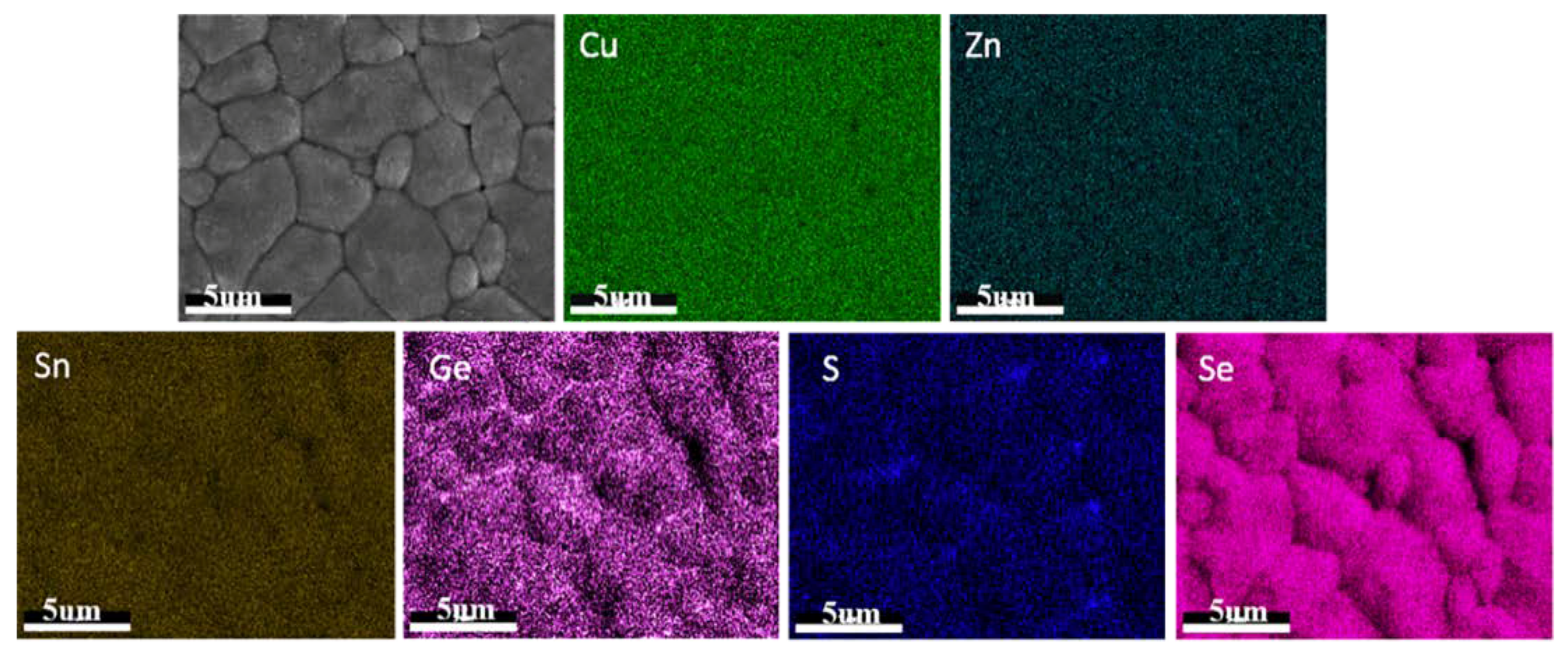
Figure 5.
(a) J–V curve, (b) external quantum efficiency (EQE), and (c) band-gap estimation for CZTSSe and CZTGSSe solar cells.
Figure 5.
(a) J–V curve, (b) external quantum efficiency (EQE), and (c) band-gap estimation for CZTSSe and CZTGSSe solar cells.

Figure 6.
J–V analysis of the CZTSSe and CZTGSSe solar cells: (a) Gsh; (b) Rs and A; (c) J0 and A.


Table 1.
Composition of the precursor film, CZTSSe film, and CZTGSSe film.
| Samples | Cu (at.%) | Zn (at.%) | Sn (at.%) | Ge (at.%) | S (at.%) | Se (at.%) | Cu/(Zn + Sn + Ge) | Zn/(Sn + Ge) | Ge/(Sn + Ge) |
|---|---|---|---|---|---|---|---|---|---|
| Precursor | 19.6 | 14.0 | 13.3 | – | 53.1 | – | 0.72 | 1.05 | – |
| CZTSSe | 21.9 | 15.1 | 12.3 | – | 3.8 | 46.9 | 0.80 | 1.23 | – |
| CZTGSSe | 20.3 | 14.9 | 9.4 | 5.5 | 3.6 | 46.3 | 0.68 | 1.00 | 0.37 |
© 2018 by the authors. Licensee MDPI, Basel, Switzerland. This article is an open access article distributed under the terms and conditions of the Creative Commons Attribution (CC BY) license (http://creativecommons.org/licenses/by/4.0/).
Share and Cite
MDPI and ACS Style
Gao, C.; Sun, Y.; Yu, W. Influence of Ge Incorporation from GeSe2 Vapor on the Properties of Cu2ZnSn(S,Se)4 Material and Solar Cells. Coatings 2018, 8, 304. https://doi.org/10.3390/coatings8090304
AMA Style
Gao C, Sun Y, Yu W. Influence of Ge Incorporation from GeSe2 Vapor on the Properties of Cu2ZnSn(S,Se)4 Material and Solar Cells. Coatings. 2018; 8(9):304. https://doi.org/10.3390/coatings8090304
Chicago/Turabian StyleGao, Chao, Yali Sun, and Wei Yu. 2018. "Influence of Ge Incorporation from GeSe2 Vapor on the Properties of Cu2ZnSn(S,Se)4 Material and Solar Cells" Coatings 8, no. 9: 304. https://doi.org/10.3390/coatings8090304
Note that from the first issue of 2016, this journal uses article numbers instead of page numbers. See further details here.