Article

Influence of External Gaseous Environments on the Electrical Properties of ZnO Nanostructures Obtained by a Hydrothermal Method

by
Marcin Procek
1,*,
Tadeusz Pustelny
1 and
Agnieszka Stolarczyk
2
1
Department of Optoelectronics, Silesian University of Technology, 2 Krzywoustego St., 44-100 Gliwice, Poland
2
Department of Physical Chemistry and Technology of Polymers, Silesian University of Technology, 9 Strzody St., 44-100 Gliwice, Poland
*
Author to whom correspondence should be addressed.
Nanomaterials 2016, 6(12), 227; https://doi.org/10.3390/nano6120227
Submission received: 7 October 2016 / Revised: 10 November 2016 / Accepted: 18 November 2016 / Published: 29 November 2016
(This article belongs to the Special Issue Semiconductor Nanoparticles for Electric Device Applications)

Abstract

:
This paper deals with experimental investigations of ZnO nanostructures, consisting of a mixture of nanoparticles and nanowires, obtained by the chemical (hydrothermal) method. The influences of both oxidizing (NO2) and reducing gases (H2, NH3), as well as relative humidity (RH) on the physical and chemical properties of ZnO nanostructures were tested. Carrier gas effect on the structure interaction with gases was also tested; experiments were conducted in air and nitrogen (N2) atmospheres. The effect of investigated gases on the resistance of the ZnO nanostructures was tested over a wide range of concentrations at room temperature (RT) and at 200 °C. The impact of near- ultraviolet (UV) excitation (λ = 390 nm) at RT was also studied. These investigations indicated a high response of ZnO nanostructures to small concentrations of NO2. The structure responses to 1 ppm of NO2 amounted to about: 600% in N2/230% in air at 200 °C (in dark conditions) and 430% in N2/340% in air at RT (with UV excitation). The response of the structure to the effect of NO2 at 200 °C is more than 105 times greater than the response to NH3, and more than 106 times greater than that to H2 in the relation of 1 ppm. Thus the selectivity of the structure for NO2 is very good. What is more, the selectivity to NO2 at RT with UV excitation increases in comparison at elevated temperature. This paper presents a great potential for practical applications of ZnO nanostructures (including nanoparticles) in resistive NO2 sensors.

Graphical Abstract

1. Introduction

Within the group of nanostructured semiconductors with a wide band gap, zinc oxide (ZnO) is a material which has been comprehensively investigated due to its interesting physical and chemical properties and the possibility of its potential extensive application in solar cells, ultraviolet (UV) photodetectors, and light emitters [1,2,3,4]. ZnO is an n-type semiconductor with a band-gap exceeding 3 eV. ZnO crystallizes in three forms: hexagonal (wurtzite), regular (zinc blende), and rarely observed regular (rock-salt) [5]. The wurtzite structure [6,7] is the most stable and the most common form of ZnO and it is most often used in ZnO based gas sensors [8]. The wurtzite structure belongs to the spatial group of C46V. The tetrahedral system of nodes is typical for covalent binding with sp3 hybridization. In the case of ZnO, the binding type has only partly covalent character, with participation of ion bindings. [9]. The conduction band of ZnO is mainly formed by orbitals 4s Zn2+, and the valence band forms 2p O2−. ZnO, like other semiconductor compounds from the II–VI group, has a simple energetic band-gap.
There are many approaches of synthesis of ZnO nanostructues described in the literature. Primary synthesis methods include chemical vapor deposition (CVD) [10], metal organic CVD [11], thermal evaporation [12], the template method [13], electrochemical deposition [14], and the laser ablation method [15]. In recent years much interest has been devoted to ZnO nanostructures obtained by means of chemical methods, mainly participation, sol-gel, and hydrothermal methods [16,17,18,19,20,21,22,23,24,25].
Detection and measurement of concentrations of toxic gases such as NO2 or NH3 and explosive gases e.g. H2 have become a necessity due to environmental protection and public safety [26,27]. Also the humidity effect on the gas sensing structures has to be taken into account due to its different values under real operating conditions [28]. Many publications emphasized the potential of ZnO nanostructures in gas sensors [8,25,27,29,30].
ZnO nanostructures gas sensing properties have been tested both theoretically and experimentally [31,32,33,34,35]. The investigations concerning gas sensors based on ZnO are already well advanced [20,29,36]. Generally, those structures are tested at elevated temperature (from 200 °C even up to 700 °C) [18,36].
Due to the extended surface of the ZnO nanostructures it ought to be stressed that their electrical properties depend considerably on the surface phenomena and electrical contact between them. On the surface of ZnO nanostructures, energy states result from the breaking of chemical bonds and creation of oxygen vacancies. The surface potential (Vs) of the nanostructure determines the curvature of the energy bands on its surface. It follows that between nanostructures the potential barriers, which determine the character of the flow of an electric current, are formed. The classical division of nanostructures distinguishes big grains, where zg > λD and small grains zg < λD, where zg indicates the size of nanograins and λD is the Debye’s shielding radius [31]. The shielding radius λD depends strongly on the concentration of electrons in the bulk nB. In the case of ZnO nanoparticles proceeds: λD = 1 nm for nB = 1018 cm−3; λD = 3 nm for nB = 1017 cm−3; λD = 10 nm for nB = 1016 cm−3.
The conductivity in structures comprising both large and small grains is a combination of so-called over-barrier and channel conductivities [34]. Theoretical analyses [34,37] indicate that the electric conductivity of a semiconductor nanostructure decreases exponentially with increasing surface potential barriers (eVs).
The present paper deals with ZnO nanostructures obtained by means of the hydrothermal method composed of nanograins and nanowires (small and large grains). The aim of our study was to investigate the electrical properties of such nanostructures in different gaseous and external conditions. The resistance of ZnO nanostructures affected by various gaseous environments (oxidizing NO2 and reducing gases: H2, NH3) was tested. The effects of carrier gas (nitrogen and air), humidity, temperature, and electromagnetic irradiation to the resistance of the structure were examined. The investigated material showed promising NO2 sensing properties at RT with ultraviolet excitation and at elevated temperature (200 °C).
With this approach, objective results and conclusions were obtained about the influence of gaseous environments, not only qualitatively, but also quantitatively. Thus, the results of the experimental investigations are of particular importance.

2. Experimental

2.1. Synthesis of ZnO Nanostructures

ZnO nanostructures were obtained by means of the hydrothermal method with ethylenediamine precursor (EDA). The following materials were used: Zn(NO3)2·6H2O, EDA (produced by Simga Aldrich, Saint Louis, MO, USA). NaOH, and ethanol (produced by POCH, Gliwice, Poland).
In a teflon vessel, 0.600 g NaOH and 0.440 g Zn(NO3)2·6H2O were dissolved in 3 mL of deionized water. Then 30 mL ethanol, 5 mL deionized water, and 5 mL EDA were added. Under these conditions ZnEDA complex was formed according to the reaction (Equation (1)) [38].
Zn2+ + 3H2NCH2CH2NH2 ↔ [Zn(H2NCH2CH2NH2)3]2+
The solution was placed for 30 min in an ultrasonic bath and then passed to an autoclave. The reaction was run for two hours at a temperature of 180 °C. Above 100 °C decomposition of ZnEDA complex occurs due to chemical equilibrium shift to the left side of the reaction (Equation (1)) [38]. Elevated temperature causes the hydrolysis of EDA and increases OH concentration (Equation (2)).
H2NCH2CH2NH2 + 2H2O → H3NCH2CH2NH2 + 2OH
In such a hydrothermal process Zn(OH)2 and next ZnO were formed according to (Equation (3)).
Zn2+ + OH → Zn(OH)2 → ZnO
After the reaction in the autoclave, the product was cooled down, the sediment was centrifuged, repeatedly rinsed in deionized water and ethanol. The zinc oxide was dried for 12 h under reduced pressure (15 mbar) at a RT.

2.2. Material Characterization Details

After the syntheses, the ZnO structures were analyzed by means of a field emission scanning electron microscope (FE-SEM) SUPRA 35 (Carl ZEISS, Jena, Germany).
To explain the molecular nature of the resulting ZnO nanostructures, they were tested by applying Raman spectroscopy. Raman investigations were made using the Ntegra Spectra system (NT-MDT, Moscow, Russia), a microscope equipped with a CCD (Charge Coupled Device) detector using green (532 nm) laser excitation.
To determine the crystal nature of the ZnO nanostructures, X-ray powder diffraction (XRD) measurements were made. XRD was investigated using a diffractometer X’Pert Pro MPD (PANAlytical, Almelo, Netherlands), containing a cobalt lamp with the main wavelength of 0.179 nm (K-alpha line) in its spectrum.
For the inspection of the grains’ distribution on the transducer a scanning electron microscope (SEM) Inspect S50 (FEI, Hillsboro, OR, USA) was used.

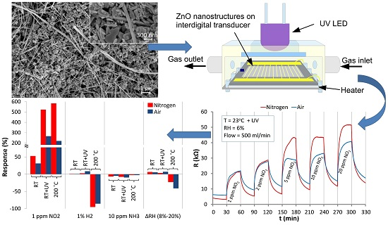
2.3. Fabrication of Resistive Structures Based on ZnO Nanostructures

In order to investigate the electrical properties of ZnO nanostructures, a resistive structure on an interdigital transducer (IDT) was made. ZnO nanostructures were deposited on an IDT by means of a drop coating method. The transducer was obtained using the photolithography method, from a 300 nm thick gold layer on a silicon substrate with a 1 μm SiO2 layer. The width of the electrodes (including the distance from each other) was 5 μm. The dimensions of the transducer were 10 × 10 mm. For the purpose of depositing ZnO nanostructures on the substrate, they were dispersed in pure hexane (produced by POCH, Gliwice, Poland) by means of an ultrasonic bath (the mixing lasted 5 min). Next the suspension was dropped onto the transducer and dried at RT. The material not adhering to the substrate was removed using compressed air with a pressure of 10 bar. Prior to the measurements, the structure was heated up to a temperature of 200 °C to remove the retained dispergent and to let the structure dry.
Three such sensing structures were fabricated and tested, all of them gave similar results and had similar properties. In order to compare the reaction of the ZnO nanostructures affected by external atmospheres, temperature and light excitation the results for the same structure are presented in the text.

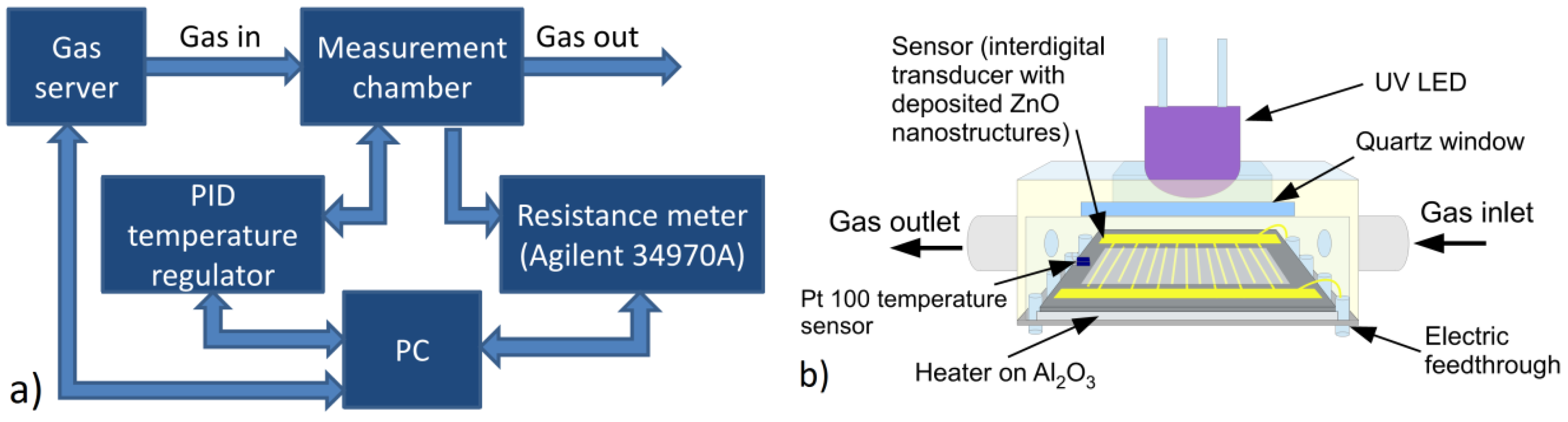
2.4. Gas Measurement Details

ZnO nanostructures were investigated in various gaseous atmospheres and under various environmental conditions (at different temperature and UV lighting). This required a special measuring chamber, in which the transducer with the deposited ZnO nanostructures was placed (Figure 1b). This measuring chamber can heat the structure by means of a thick-layer heater on an Al2O3 substrate and can measure the temperature by a Pt-100 sensor. A quartz window and an ultraviolet LED (λ ≈ 390 nm) permits the illumination of the sample by means of UV radiation. The transducer mounted on the heater was mobilized on a special chip, and the contacts between its leg and the transducer electrodes were constructed by means of wire bonding (gold wire with a diameter of 25 μm) using the bonder 53XX-BDA (made by F&K DELVOTEC, Braunau, Austria). The cover of this chamber consists of PTFE and is equipped with fast gas connectors of stainless steel. The block scheme of the measurement setup is shown in Figure 1a. The acquisition of data and control of the measurements were accomplished by a PC. The temperature was controlled and measured by the PID controller SR94 (produced by Shimaden, Tokyo, Japan). In all these cases, the resistance was measured making use of a multichannel switch unit 34970A (produced by AGILENT, Santa Clara, CA, USA).
The applied gaseous mixtures were produced by a gas server allowing precise preparation of the gaseous atmospheres, composed of any kind of carrier gas and up to five different gases of precisely determined concentrations. The gas server was described in an earlier paper [39].
The flow of gas through the measuring chamber was constant for all the measurements (500 mL/min). During the measurements two different gases were applied as the atmosphere (carrier gases), viz. nitrogen 6.0 and synthetic air (O2: 20%; N2: 80%). Their relative humidity was the same, amounting to about: 6% ± 1% (at 22 °C). In the experiments, adequate standard gases were used, viz. H2: 99.9994%; NO2: 100 ppm in N2; NH3: 500 ppm in air. The humidity of the gas was changed by means of a bubble humidifier and monitored by an RH meter. The measurement of the response of the ZnO nanostructures to the effect of the gases consisted in alternating the introduction of pure carrier gas into the measuring chamber and the tested gas with the given concentration in the atmosphere (synthetic air or nitrogen N2). In each successive cycle, the concentration of the gas was raised. The measurements were performed at RT = 23 °C, at elevated temperature of T = 200 °C and also when illuminating the sample of ZnO nanostructure by UV light at RT.
The structure responses to a given gases were calculated according to the formula:
R e s p o n s e = R g R a R a 100 % ,
where Ra is the sensor resistance in the carrier gas and Rg is the sensor resistance after the action with the selected gas.

2.5. Details Concerning Spectral Measurements

The dependence of the resistance of ZnO nanostructures on the wavelength of optical excitation was measured. The resistance of the ZnO nanostructures was measured during illumination with light in the range from 300 nm to 750 nm. The source of light was a xenon lamp, and the wavelength was measured by tuning the monochromator DH-10 (made by Jobin Yvon, Lonjumeau, France). In this case, the measurements were performed in atmospheric air, at RT. The intensity of light was kept at a constant level and monitored by a spectrometer HR 2000 + ES (made by Ocean Optics, Dunedin, FL, USA).

2.6. Details Concerning the Temperature Measurements

Investigations of the dependence of the resistance of ZnO nanostructures on temperature R(T) in various gaseous atmospheres, viz. synthetic air and nitrogen, were performed. In each series of tests, the sample was prepared by heating in a given carrier gas up to 300 °C and then cooling down to RT. The resistance was recorded for other temperature cycles of heating and cooling in the given atmosphere. The temperature was changed within the range of 40–300 °C every 10 °C until the resistance became stable (the interval of time was equal to about Δt = 2 min).

3. Results and Discussion

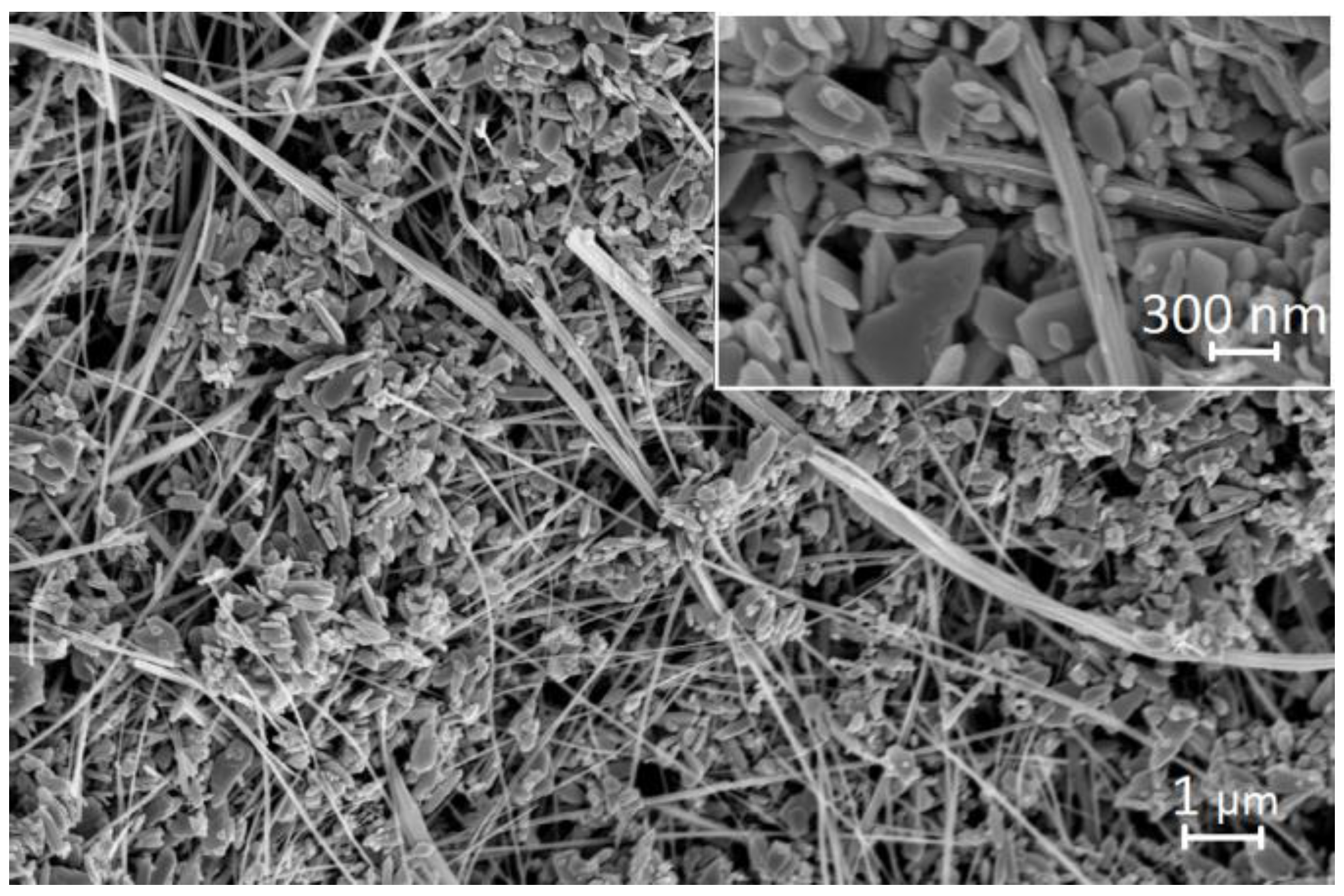
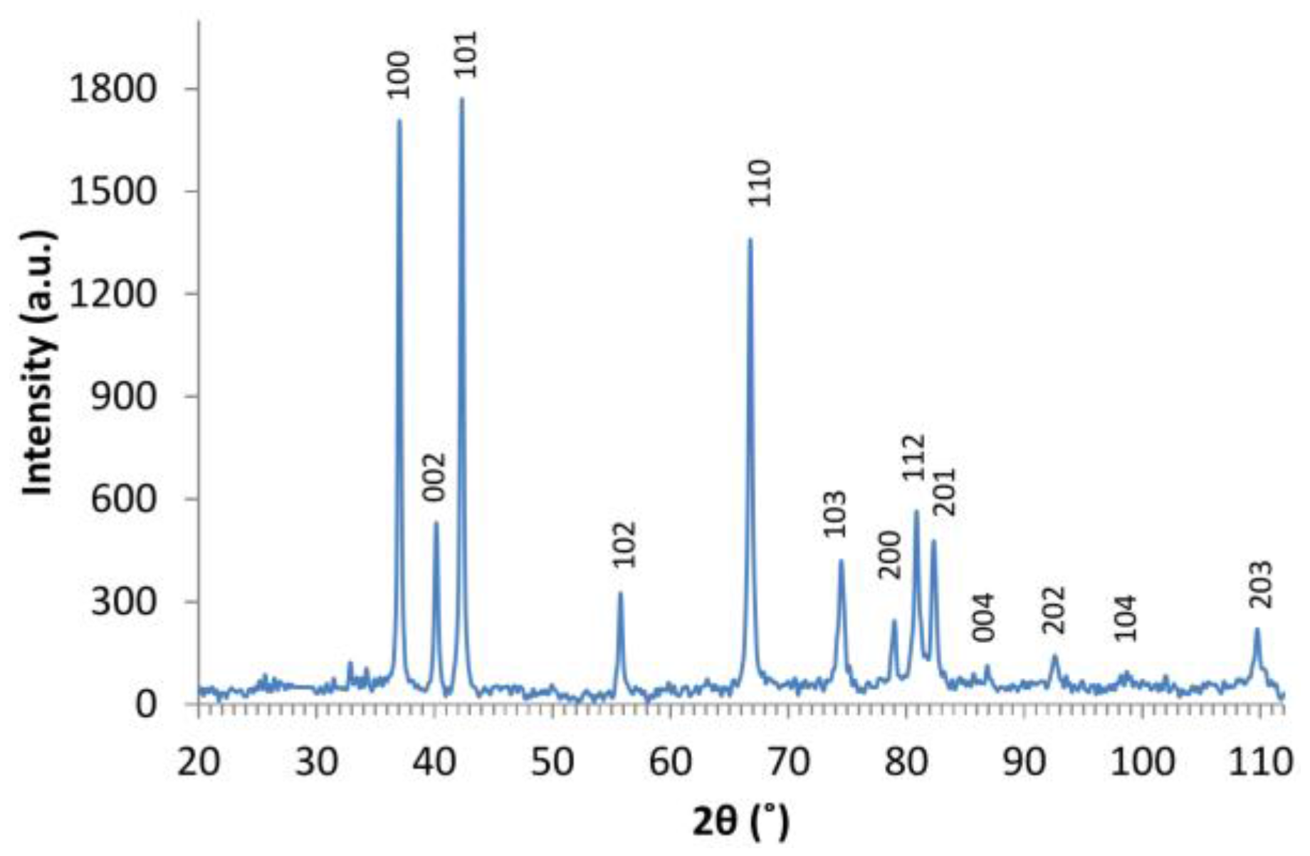
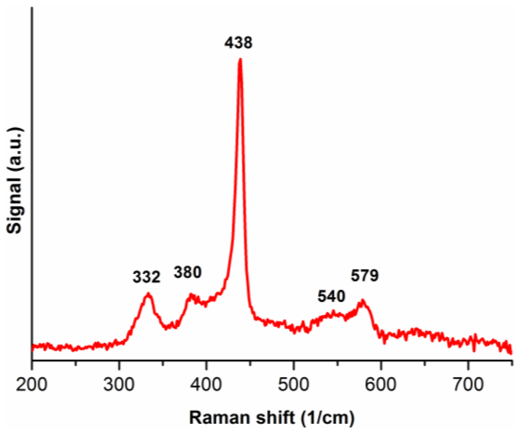
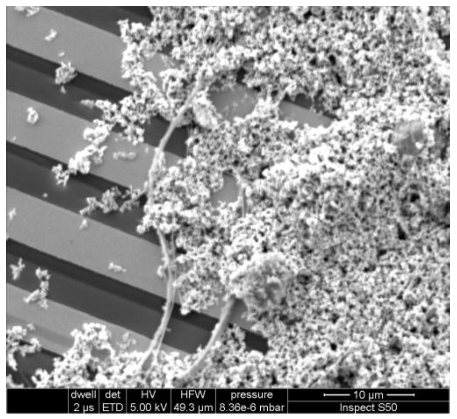
3.1. ZnO Structures Characterization

Morphology of the ZnO structures is presented on FE-SEM images in Figure 2. The nanostructures of ZnO obtained by the hydrothermal method constitute a rich mixture of different geometrical forms, from nanobars and nanotubes, most with lengths up to a few µm up to nanoparticles such as nanolumps with sizes of a few nm. From the physical point of view, a division of nanostructures into the so-called large and small ones is reasonable [31]. In our case, the large geometrical variety of ZnO nanostructures and the wide range of their sizes require them to be treated as a mixture of both large and small nanostructures.
The XRD results are shown in Figure 3. The obtained diffractogram is characteristic for the hexagonal structure of ZnO with the spatial group P63mc (patterns are consistent with the ICSD card at the code No. 180052 titled ”Zinc Oxide–Nanoparticles”). In the spectrum, no additional peaks could be detected. The average crystal sizes estimated from XRD patterns using the Scherer equation [40] are in the range of 227 nm (for crystallographic plane (100)) to 3 nm (for plane (203)). The obtained results confirm conclusions from FE-SEM where mixtures of structures with different shapes were observed.
Figure 4 presents the Raman spectrum of ZnO nanostructures. The obtained spectrogram is compatible with Raman peak values for ZnO nanocrystals given in the reference [6] with slight drift (in the range of 2–5 cm−1) caused by different crystals sizes. In this case all the atoms occupy C3v sites. Group theory shows that active Raman modes are A1+E1+2E2. The phonons of A1 and E1 symmetry are polar phonons and, hence, exhibit different frequencies for the transverse-optical (TO) and longitudinal-optical (LO) phonons [6]. Raman modes at 332, 380, 438, 540 and 579 cm−1 are denoted as 2E2, E1(TO), E2, A1(LO) and E1(LO) modes, respectively.
ZnO nanostructures deposited on the IDT have a relatively uniform distribution and good adhesion to the substrate, as may be observed on the SEM image in Figure 5. The adhesion of the nanostructures to the transducer is the result of van der Waals and electrostatic forces. Thus, small grains which have smaller mass to contact area ratio have better adhesion than bigger ones. Long nanowires which have contact to a few electrodes stabilized the electrical properties of the sensor structure. Thanks to the mixture of small grains and nanowires, layers with good adhesion and electrical stability were obtained. The thickness of the layer is not uniform and its value is in the range from single crystalline size up to single micrometers (Figure 5).

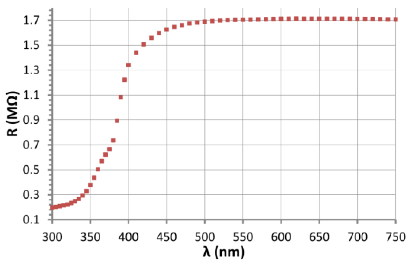
3.2. Investigations of the Influence of Light on the Resistance of ZnO Nanostructures

The results of spectral tests R(λ) are gathered in Figure 6. Changes of the resistance are observed in the range between 300 and 500 nm. Below 380 nm the resistance changes are smaller. The characteristics show the existence of an absorption edge in the ZnO nanostructures somewhere about 380 nm. In crystalline ZnO the absorption edge (corresponding to the band gap) is also observed at about 380 nm [9], which corresponds to an energy ΔE of 3.25 eV.
The decrease of the resistance under UV irradiation is mainly caused by the increase in the concentration of the electrical charges (electrons and holes), as a result of photogeneration as well as excitation of electrons from the surface states. Of no less importance is the phenomenon of photocatalysis leading to the desorption of the gases (especially oxygen) absorbed (in the form of molecules, atoms, and ions) on the surface active centers of the ZnO nanostructures [41].

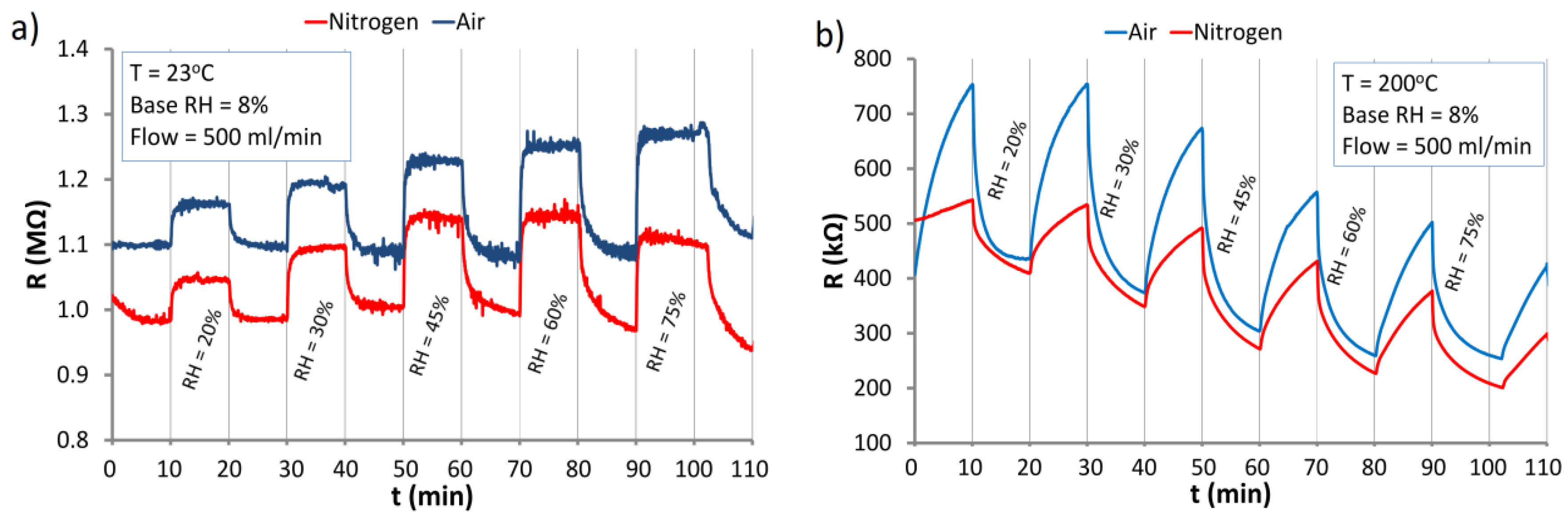
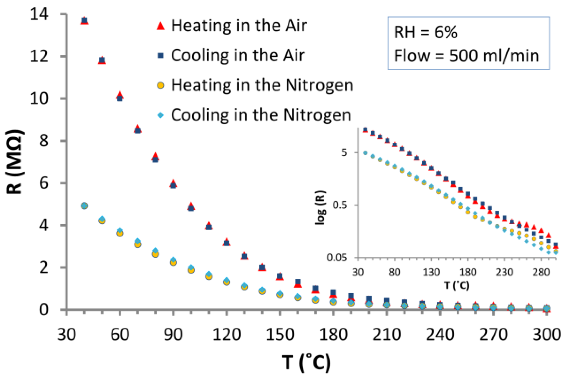
3.3. The Effect of the Carrier Gas and Temperature on the Electrical Properties of ZnO Nanostructures

The authors attempted to explain experimentally to what extent the oxygen contained in the air affects the interaction of the tested gases with ZnO nanostructures. Figure 7 illustrates the dependence of the electrical resistance on the temperature of the layer of ZnO nanostructures in atmospheres of synthetic air and in nitrogen.
The diagram of R(T) (Figure 7) shows the differences between the resistance values in both carrier gases during cooling and heating the sample. It is particularly noticeable in the temperature range from 40–180 °C. It can be seen in Figure 7 that at the measured temperature range the resistance of ZnO nanostructures is higher in air (in the presence of oxygen) than that in nitrogen. An increase in the temperature reduces the resistance of the nanostructures. It is the effect of a decrease of the concentration of electrons in the surface states and the reduction of the surface potential barriers of ZnO nanostructures. In the nitrogen atmosphere the created oxygen vacancies stay unoccupied.

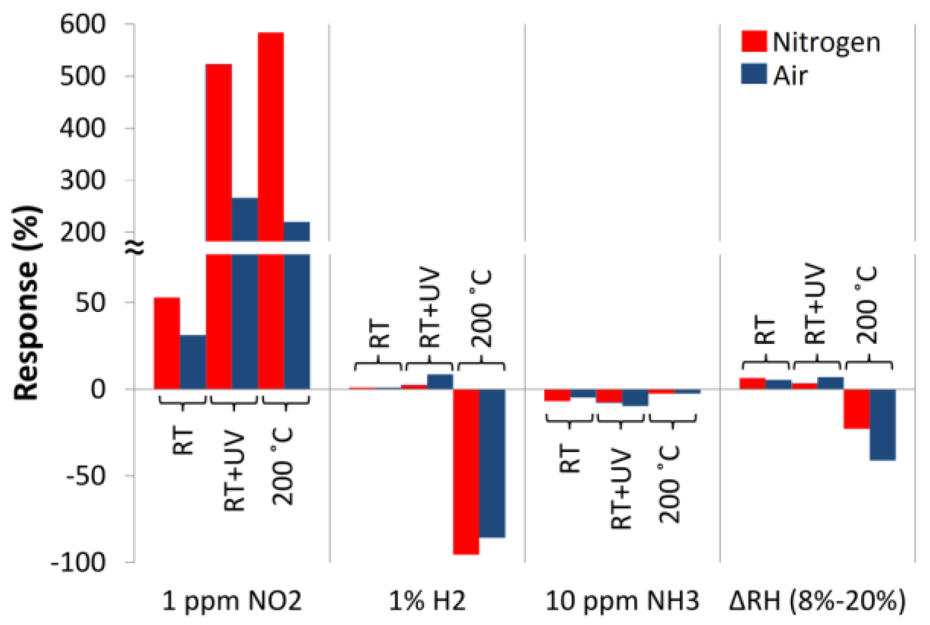
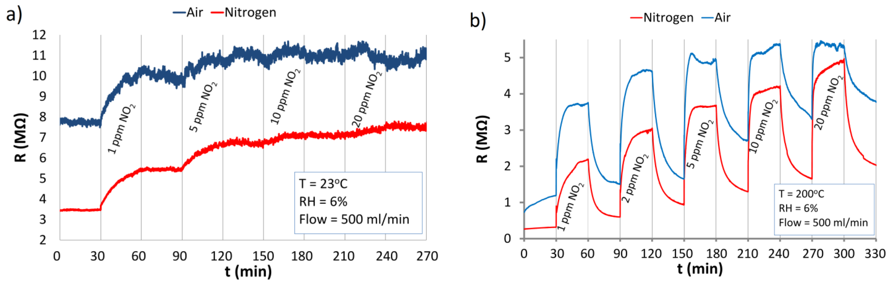
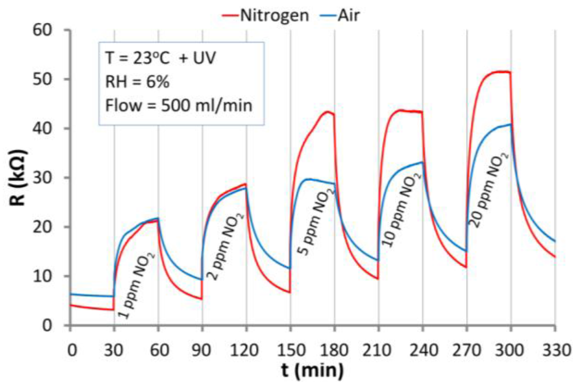
3.4. The Reaction of ZnO Nanostructures to NO2

As an example of oxidizing gas small concentrations of NO2 (1–20 ppm) were chosen.
The characteristics shown in Figure 8a prove that at RT ZnO nanostructures reacted to NO2 only in the first cycle (1 ppm) where their resistance increased by c.a. 50% in N2 and 30% in air. When the resistive ZnO structure was “saturated” its further exposure to NO2 action at RT did not result in a change of the resistance. At RT, when NO2 was removed from the carrier gas, the structures did not recover, and the resistance of the structure did not return to its initial values. The results at 200 °C are presented in Figure 8b. Heating the structure up to 200 °C resulted in a strong increase of the response of ZnO nanostructures to NO2. In this case responses to 1 ppm of NO2 were c.a. 600% in nitrogen and c.a. 230% in air. At the elevated temperature, sensor recovery is observed (Figure 8b), which is caused by the desorption of NO2 from the ZnO nanostructures. It is revealed by the decrease in the resistance after each NO2 exposure.
The elevated temperature (200 °C) of the structure leads to an increase in free chemical bonds (oxygen vacancies) on the surface of ZnO nanostructures, which can bind with gas molecules. The changes of the resistance of the structures depend also on the concentration of electrons, which are thermally transferred from traps localized in the band-gap to the conduction band. Therefore, the spatial distribution of electrical charges in the ZnO nanostructures is also changed. The temperature of about 200 °C also facilitates desorption of the NO2 from the active centers. The investigations showed that detoxication after 1 ppm of NO2 exposure of the structure requires a longer time in an atmosphere of synthetic air (t90% = 880 s) than in nitrogen (t90% = 700 s). In an atmosphere of air, active centers can join to both NO2 and oxygen simultaneously [34,42,43].
The differences between the structure reaction to NO2 at RT and elevated temperature can be explained by a chemical mechanism of this interactions. At RT, NO2 is absorbed by ZnO nanostructures mainly in the form of NO3 ions with evacuation of gaseous NO [8,44]. At the elevated temperature, the absorbed NO3 undergoes decomposition to gaseous NO2 and adsorbed O. As NO2 and its derivatives are oxidizing gases, they incorporate electrons from the ZnO nanostructures, which increase their resistance.
The results of the response of ZnO nanostructures to NO2 in air and nitrogen atmospheres under UV illumination and at RT are shown in Figure 9. Resistance of the structure increases proportionally to NO2 concentration. The structure responses to 1 ppm of NO2 amount to 430% in N2 and 340% in the air. Under this conditions in both carrier gases structure recovery occurs, which proves that UV illumination allows a desorption of NO2 from the ZnO nanostructures at RT.
The excitation of ZnO nanostructures by means of UV radiation causes both photogeneration of electron-hole pairs, and generation of charge carriers from the surface states. On the ZnO surface the photocatalytic reactions of the adsorption (with capture of electron) and desorption (with capture of hole) of oxygen can occur [45].
In the case of air conditions both reactions occur and the surface potential is the result of equilibrium between them. In nitrogen only oxygen desorption occurs, and thus the surface potential is smaller than in air. This can be observed in the differences of base resistances under both conditions (Figure 9). This phenomenon has also impact on the kinetics of the reaction of the structure with NO2. Due to the higher oxygen vacancy concentration in nitrogen the structure response is higher than under air conditions.
The presented results prove that UV excitation enables ZnO nanostructures to respond and recover at RT. Under air conditions the structure response is higher at RT with UV activation than at elevated temperature. This makes UV excited ZnO nanostructures promising materials for low concentration NO2 sensors operating at RT.

3.5. Reactions of ZnO Nanostructures with Reducing Gases

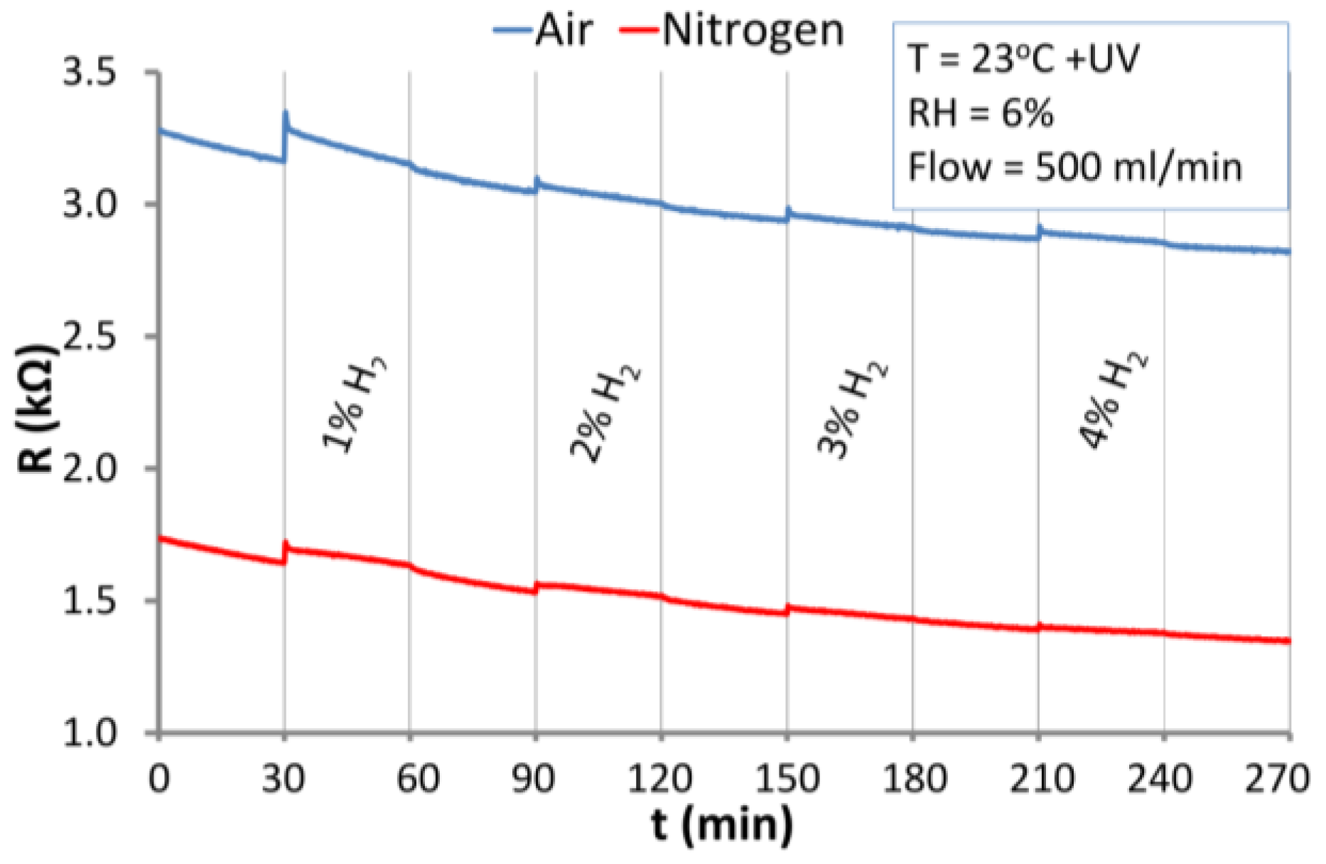
3.5.1. The Reaction of ZnO Nanstructures with Hydrogen

The reaction of ZnO nanostructures with H2 in an atmosphere of synthetic air and nitrogen at RT and at 200 °C is presented in Figure 10. The structure was exposed to relatively high concentrations of hydrogen in the range of a few percent (1% ≡ 104 ppm). The detection of such high H2 concentrations is important because hydrogen is explosive at 4% concentration in air.
At RT (Figure 10a) no reaction of the ZnO nanostructures to H2 was observed. Contrary to RT, at elevated temperature (200 °C) under both atmospheres (Figure 10b) a relatively high and fast response to hydrogen was observed. The response is characteristic of reducing gases, which decrease the resistance of n-type semiconductors. In comparison to adsorption, the rate of desorption at 200 °C is rather slow, especially under nitrogen atmosphere. Due to the relatively high concentrations of H2, there are very small differences between the responses to various concentrations. A temperature of 200 °C seems to be high enough for reversible adsorption of dissociatively chemisorbed hydrogen to occur. Adsorption of H2 results in the formation of a H–O–ZnO surface [46]. The response of ZnO nanostructure at 200 °C is relatively fast because of the high concentration of H2 and the small size of hydrogen molecules. The hydrogen ions react with oxygen ions on the ZnO surfaces and may cause desorption of oxygen from active centers and the ZnO lattice [25,29]. This results in a decrease in the potential barriers between nanograins and thus the resistance of the sensor structure is reduced. The desorption process is faster in air than in nitrogen (Figure 10b). The oxygen from the air leads to a re-oxidation of the oxide vacancies on the surface of ZnO nanostructures during recovery of the structure. In the nitrogen atmosphere, the resistive structure recovers very weakly due to the absence of oxygen (or other oxidizing analytes) which can fill the vacancies created by hydrogen. Therefore the role of oxygen from the air is important in the sensor recovery process.
The reaction of ZnO nanostructures to H2 under continuous UV irradiation at RT is presented in Figure 11. Similar to dark conditions (Figure 10a), the resistive structure practically does not react to hydrogen at RT. Under UV radiation in both carrier gases, only small changes of resistance were observed directly after letting H2 into the chamber (Figure 11). This could be the effect of the change in oxygen concentration or RH after mixing H2 with the carrier gas. Hydrogen also has a very high heat conductivity, and at such high concentration can cause small local changes in the temperature of the ZnO resistive structure.
Due to the fact that the concentrations of hydrogen in the atmosphere of air were high, the saturation of the structure by hydrogen (H2, H+) is evident in the diagram in Figure 10b. The reaction of the ZnO nanostructure with 1% and 4% hydrogen is similar. At RT, the structure is not sensitive to the presence of hydrogen, even after optical excitation (Figure 11). The H2 molecules are not very reactive under standard conditions (the orbital s of the H2 molecule is complete).

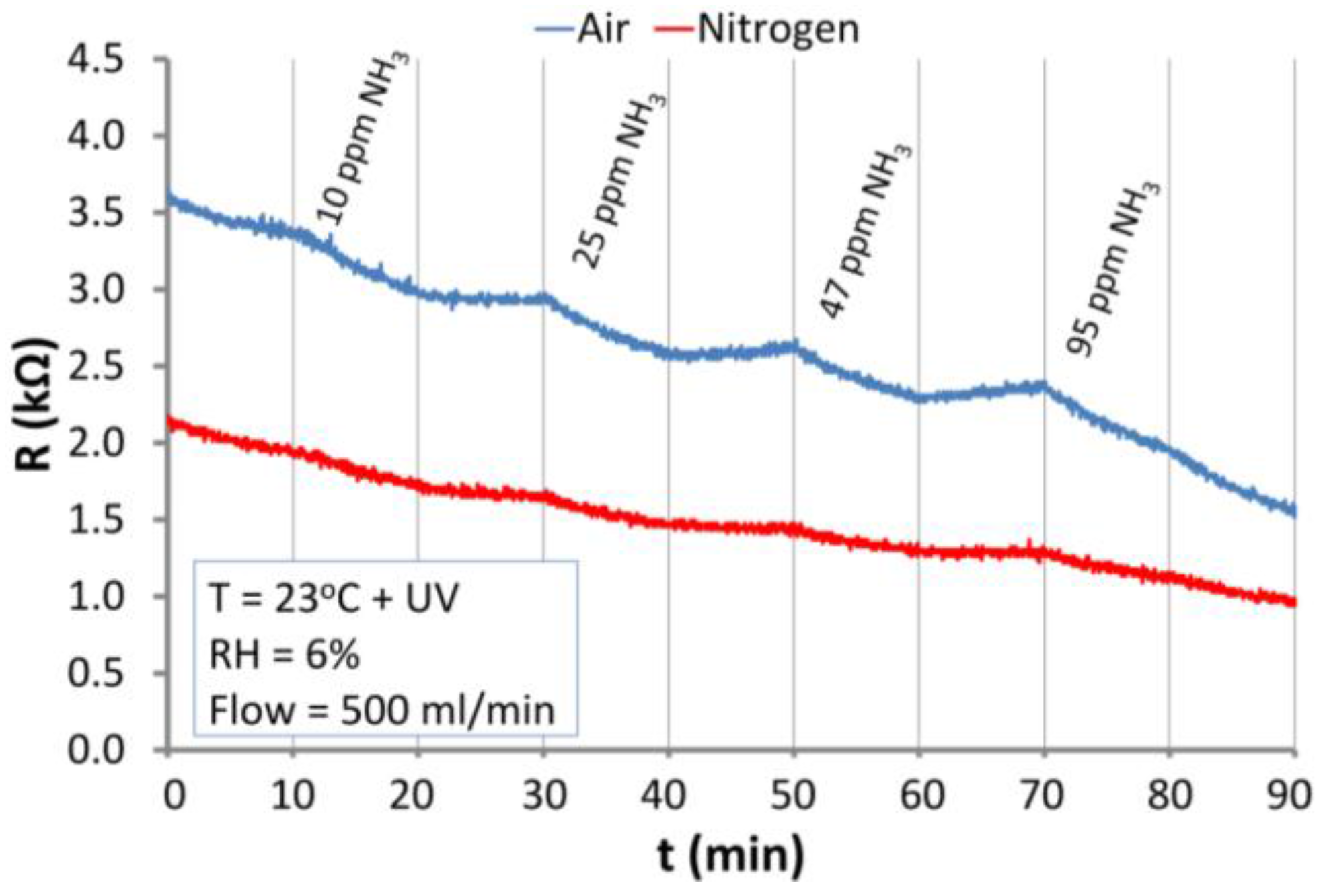
3.5.2. The Reaction of ZnO Nanostructures with Ammonia

The results of the investigations of the reaction of the structure to NH3 are shown in Figure 12. At RT, NH3 reacts with the ZnO nanostructures only slightly, decreasing the resistance of the ZnO structure (Figure 12a). In both atmospheres at RT, the reaction of ZnO nanostructures with ammonia is negligible and desorption is practically undetectable. At elevated temperature (200 °C), the ZnO nanostructures react distinctly with NH3 under both atmospheres (Figure 12b).
Similar to the case of H2, the interactions of ZnO nanostructures with NH3 were typical for reducing gases (resistance decreases). At the elevated temperature, a relatively fast desorption took place in the atmosphere of air and a comparably slow one in the nitrogen atmosphere. Figure 13 presents the sensitivity of the optically excited (UV) ZnO nanostructures exposed to ammonia in air and nitrogen atmospheres at RT.
It ought to be stressed that in spite of the similar character of the behavior of ZnO nanostructures exposed to NH3 and H2, the range of changes differs, taking into account the many times smaller concentrations of ammonia.

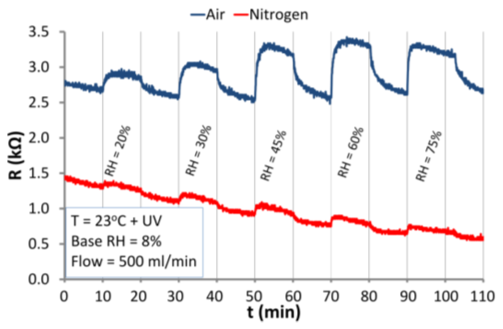
3.6. The Response of ZnO Nanostructures to Changes of the Humidity

Figure 14 presents the reaction of ZnO nanostructures to changes of the RH level under atmospheres of air and nitrogen. The tests were performed at RT (23 °C) and elevated temperature of 200 °C.
The investigations (Figure 14) proved that the ZnO nanostructures are sensitive to humidity even at RT. It ought to be stressed that their response to RH reveals a different direction of resistance change, depending on the temperature at which the measurements were taken. At RT water is physically absorbed by ZnO nanostructures due the dipole character of the water molecules. The water molecules are absorbed by ZnO nanostructures as a result of van der Waals forces as well as, in some steps, by electrostatic forces. The polarity of H2O molecules changes the distribution of the electrical charges on the surface of ZnO nanostructures, therefore the resistance increases with increase in RH. This indicates that at low temperatures no dissociative adsorption of H2O molecules on ZnO surface takes place. The H2O dissociation can be observed at elevated temperatures from about 150 °C upwards [32]. This is connected with the supply of electrical charges to ZnO nanostructures and the neutralization of some part of the adsorbed oxygen molecules and lattice oxygen (caused by the reaction of H+ with O). This leads to increasing the concentration of charge carriers. As an effect of this increase, the resistance of the structure drops, as can be seen in Figure 14b. At the temperature of about 200 °C, the effect of the dissociation of water on the electrical properties of ZnO nanostructures dominates. The investigations showed that at the temperature exceeding 200 °C humidity is chemisorbed (hydroxyl groups are joined to the ZnO nanostructures [31]).
Under UV irradiation at RT (Figure 15), the sensor reacts similarly to the dark conditions at RT (Figure 15a). An increase in the RH level indicates the increase in the resistance of ZnO nanostructures. That proves that UV radiation does not cause dissociative chemisorption of water. As in the case of dark conditions under UV irradiation physical adsorption occurs. In the atmosphere of nitrogen, the structure reacts to RH changes weaker than in the atmosphere of air. This can be explained by the lower concentration of negatively charged oxygen adsorbed on the surface in the presence of nitrogen.

4. Summary and Conclusions

The aim of our study was to investigate the electrical properties of ZnO nanostructures obtained by the hydrothermal method composed of nanograins and nanowires (small and large grains) in different gaseous and external conditions. The effects of different gases, carrier gas (nitrogen and air), humidity, temperature, and electromagnetic irradiation on the resistance of the structure was examined. The investigated material showed promising NO2 sensing properties at RT with ultraviolet excitation and at elevated temperature (200 °C).
Our studies showed the role of atmospheric oxygen with respect to the sensitivity of the structure based on ZnO nanostructures on the effect of oxidizing and reducing gases. The experimental studies showed that the presence of oxygen in the gaseous atmosphere affects the electrical properties of the structure. The research showed that the sensitivity of ZnO nanostructures to gases depends on the temperature of these structures and their optical excitation (UV radiation).
The structure responses (Equation (1)) to all the investigated gases are summarized in Figure 16.
The results confirmed a strong increase in the responses of ZnO nanostructures at 200 °C. In dark conditions at RT the structure recovery was very weak or was not observed, whereas at 200 °C effective recovery occurred. The UV excitation of the ZnO nanostructures enabled effective recovery of the structure after its reaction with NO2 already at RT. Under UV condition at RT structure responses to NO2 are comparable with responses at 200 °C. The studies showed a limited impact of RH on the electrical resistance of ZnO nanostructures. At RT the impact of RH to the structure resistance is weaker than at elevated temperature. Also the different sorption mechanisms of the interaction of water molecules with ZnO nanostructures at RT and a temperature of 200 °C were observed (different directions of the reactions).
The interactions of ZnO nanostructures with gases showed typical reactions: their electrical conductivity increases when exposed to reducing gases (H2 and NH3), and decreases during exposure to oxidizing gases (O2 and NO2). Generally, at RT, the gas molecules interact with ZnO nanostructures primarily physically (except NO2), while at elevated temperatures, these interactions have the character of chemical adsorption [31]. It has to be stressed that the ZnO nanostructures are particularly sensitive to the presence of NO2 under both atmospheres (air and nitrogen). The response (Equation (1)) of ZnO nanostructure to the effect of NO2 at a temperature of 200 °C is more than 105 times greater than the response of NH3, and more than 106 times greater than that to H2 in the relation of 1 ppm. Thus the selectivity of the structure for NO2 is very good. What is more the selectivity to NO2 at RT with UV excitation increases in comparison to elevated temperature.
In Table 1 the comparison the response of the investigated structure to 1 ppm of NO2 to other ZnO nanostructure based gas sensors responses is presented. This comparison shows that the response of the presented structure is higher or comparable to other approaches. What is more under UV radiation high response is observed also at RT. This shows the possibility of detection of small concentrations of NO2 at RT with good sensitivity comparable to high temperature sensors (>200 °C). Operation of a potential sensor at RT ensures low energy consumption and improves the safety of its usage.
In comparison to the flower-like ZnO nanostructures which were investigated as a gas sensing material in our earlier work [21] the structure presented in this paper has better sensing properties (smaller noise level and much higher sensitivity to gases). Thanks to the use of a mixture of small grains and nanowires layers with improved adhesion and electrical stability were obtained. This proves that morphology has a very high impact on material sensing properties which are improved by the nanoparticle content in the investigated nanostructures.
It may be expected that the ZnO nanostructures allow the detection of low concentrations of NO2 in the range of ppb even at RT (with UV excitation). The investigated ZnO nanoparticles presents a high selectivity to NO2 and could be practically used as a sensor for this gas (e.g., for environmental monitoring). Such a high sensitivity of the ZnO nanostructures exposed to NO2 provides an opportunity to apply this type of ZnO nanostructures to detect vapors of explosives in the environment [54].

Acknowledgments

The work was partially financed by the Polish National Science Centre (NCN) within the grant 2012/07/B/ST7/01 471 and Silesian University of Technology, Faculty of Electrical Engineering within grants BK/232/Re4/2016 and BKM/534/Re4/2015.

Author Contributions

Marcin Procek designed and carried out the experiments, designed the experiment stand, cooperated in technology processes, made material characterization, analyzed the data, and participated in preparing the paper; Tadeusz Pustelny elaborated a concept of studies, analyzed and discussed the data, and participated in preparing the paper; Agnieszka Stolarczyk designed and dealt with the technology process and described it in the text, partially analyzed the data and participated in preparing the paper.

Conflicts of Interest

The authors declare no conflict of interest.

References

  1. Li, L.; Zhai, T.; Bando, Y.; Golberg, D. Recent progress of one-dimensional ZnO nanostructured solar cells. Nano Energy 2012, 1, 91–106. [Google Scholar] [CrossRef]
  2. Kayaci, F.; Vempati, S.; Donmez, I.; Biyikli, N.; Uyar, T. Role of zinc interstitials and oxygen vacancies of ZnO in photocatalysis: A bottom-up approach to control defect density. Nanoscale 2014, 6, 10224. [Google Scholar] [CrossRef] [PubMed]
  3. Cun, T.; Dong, C.; Huang, Q. Ionothermal precipitation of highly dispersive ZnO nanoparticles with improved photocatalytic performance. Appl. Surf. Sci. 2016, 384, 73–82. [Google Scholar] [CrossRef]
  4. Xu, L.; Zheng, G.; Wang, J.; Xian, F.; Liu, Y. Stable co-emission of UV, green and red light in ZnO thin films with rapid annealing treatment. Opt. Int. J. Light Electron Opt. 2016, 127, 5942–5949. [Google Scholar] [CrossRef]
  5. Saoud, F.S.; Plenet, J.C.; Henini, M. Band gap and partial density of states for ZnO: Under high pressure. J. Alloys Compd. 2015, 619, 812–819. [Google Scholar] [CrossRef]
  6. Ojha, A.K.; Srivastava, M.; Kumar, S.; Hassanein, R.; Singh, J.; Singh, M.K.; Materny, A. Influence of crystal size on the electron–phonon coupling in ZnO nanocrystals investigated by Raman spectroscopy. Vib. Spectrosc. 2014, 72, 90–96. [Google Scholar] [CrossRef]
  7. Morkoc, H.; Ozgur, U. Zinc Oxide: Fundamentals, Materials and Device Technology; Wiley-VCH Verlag GmbH & Co. KGaA: Weinheim, Germany, 2009. [Google Scholar]
  8. Chen, M.; Wang, Z.; Han, D.; Gu, F.; Guo, G. High-sensitivity NO2 gas sensors based on flower-like and tube-like ZnO nanomaterials. Sens. Actuators B 2011, 157, 565–574. [Google Scholar] [CrossRef]
  9. Klingshirn, C. ZnO: Material, physics and applications. ChemPhysChem 2007, 8, 782–803. [Google Scholar] [CrossRef] [PubMed]
  10. Yuan, W.; Liu, A.; Huang, L.; Li, C.; Shi, G. High-performance NO2 sensors based on chemically modified graphene. Adv. Mater. 2013, 25, 766–771. [Google Scholar] [CrossRef] [PubMed]
  11. Fanni, L.; Aebersold, B.A.; Alexander, D.T.L.; Ding, L.; Morales Masis, M.; Nicolay, S.; Ballif, C. c-texture versus a-texture low pressure metalorganic chemical vapor deposition ZnO films: Lower resistivity despite smaller grain size. Thin Solid Films 2014, 565, 1–6. [Google Scholar] [CrossRef]
  12. Rai, P.; Khan, R.; Ahmad, R.; Hahn, Y.-B.; Lee, I.-H.; Yu, Y.-T. Gas sensing properties of single crystalline ZnO nanowires grown by thermal evaporation technique. Curr. Appl. Phys. 2013, 13, 1769–1773. [Google Scholar] [CrossRef]
  13. Tian, Y.; Li, J.; Xiong, H.; Dai, J. Controlled synthesis of ZnO hollow microspheres via precursor-template method and its gas sensing property. Appl. Surf. Sci. 2012, 258, 8431–8438. [Google Scholar] [CrossRef]
  14. Bai, S.; Sun, C.; Guo, T.; Luo, R.; Lin, Y.; Chen, A.; Sun, L.; Zhang, J. Low temperature electrochemical deposition of nanoporous ZnO thin films as novel NO2 sensors. Electrochim. Acta 2013, 90, 530–534. [Google Scholar] [CrossRef]
  15. Thareja, R.K.; Saxena, H.; Narayanan, V. Laser-ablated ZnO for thin films of ZnO and MgxZn(1−x)O. J. Appl. Phys. 2005, 98, 34908. [Google Scholar] [CrossRef]
  16. Kołodziejczak-Radzimska, A.; Jesionowski, T.; Krysztafkiewicz, A. Obtaining zinc oxide from aqueous solutions of KOH and Zn(CH3COO)2. Physicochem. Probl. Miner. Process. 2010, 44, 93–102. [Google Scholar]
  17. Tong, Y.; Liu, Y.; Dong, L.; Zhao, D.; Zhang, J.; Lu, Y.; Shen, D.; Fan, X. Growth of ZnO nanostructures with different morphologies by using hydrothermal technique. J. Phys. Chem. B 2006, 110, 20263–20267. [Google Scholar] [CrossRef] [PubMed]
  18. Neri, G. First fifty years of chemoresistive gas sensors. Chemosensors 2015, 3, 1–20. [Google Scholar] [CrossRef]
  19. Pustelny, T.; Procek, M.; Maciak, E.; Stolarczyk, A.; Drewniak, S.; Urbańczyk, M.; Setkiewicz, M.; Gut, K.; Opilski, Z. Gas sensors based on nanostructures of semiconductors ZnO and TiO2. Bull. Pol. Acad. Sci. Tech. Sci. 2012, 60, 853–859. [Google Scholar] [CrossRef]
  20. Djurišić, A.B.; Chen, X.; Leung, Y.H.; Man Ching Ng, A. ZnO nanostructures: Growth, properties and applications. J. Mater. Chem. 2012, 22, 6526. [Google Scholar] [CrossRef]
  21. Procek, M.; Pustelny, T.; Stolarczyk, A.; Maciak, E. Studies of changes in electrical resistance of zinc oxide nanostructures under the influence of variable gaseous environments. Bull. Pol. Acad. Sci. Tech. Sci. 2014, 62, 635–639. [Google Scholar] [CrossRef]
  22. Wang, Y.; Ma, C.; Sun, X.; Li, H. Preparation of nanocrystalline metal oxide powders with the surfactant-mediated method. Inorg. Chem. Commun. 2002, 5, 751–755. [Google Scholar] [CrossRef]
  23. Li, P.; Wei, Y.; Liu, H.; Wang, X. Growth of well-defined ZnO microparticles with additives from aqueous solution. J. Solid State Chem. 2005, 178, 855–860. [Google Scholar] [CrossRef]
  24. Djurišić, A.B.; Chen, X.Y.; Leung, Y.H. Recent progress in hydrothermal synthesis of zinc oxide nanomaterials. Recent Pat. Nanotechnol. 2012, 6, 124–134. [Google Scholar] [CrossRef] [PubMed]
  25. Zhao, X.; Li, M.; Lou, X. Sol–gel assisted hydrothermal synthesis of ZnO microstructures: Morphology control and photocatalytic activity. Adv. Powder Technol. 2014, 25, 372–378. [Google Scholar] [CrossRef]
  26. Liu, X.; Cheng, S.; Liu, H.; Hu, S.; Zhang, D.; Ning, H. A survey on gas sensing technology. Sensors 2012, 12, 9635–9665. [Google Scholar] [CrossRef] [PubMed]
  27. Kumar, R.; Al-Dossary, O.; Kumar, G.; Umar, A. Zinc oxide nanostructures for NO2 gas–sensor applications: A review. Nano Micro Lett. 2015, 7, 97–120. [Google Scholar] [CrossRef]
  28. Fine, G.F.; Cavanagh, L.M.; Afonja, A.; Binions, R. Metal oxide semi-conductor gas sensors in environmental monitoring. Sensors 2010, 10, 5469–5502. [Google Scholar] [CrossRef] [PubMed]
  29. Abdullah, N.A.; Khusaimi, Z.; Mohammad Rusop, M. A review on zinc oxide nanostructures: Doping and gas sensing. Adv. Mater. Res. 2013, 667, 329–332. [Google Scholar] [CrossRef]
  30. Procek, M.; Pustelny, T. A study of gas sensing properties of ZnO nanostructures activated by UV light. Photonics Lett. Pol. 2015, 7, 50–52. [Google Scholar]
  31. Barsan, N.; Weimar, U. Conduction model of metal oxide gas sensors. J. Electroceram. 2001, 7, 143–167. [Google Scholar] [CrossRef]
  32. An, W.; Wu, X.; Zeng, X.C. Adsorption of O2, H2, CO, NH3 and NO2 on ZnO nanotube: A density functional theory study. J. Phys. Chem. C 2008, 112, 5747–5755. [Google Scholar] [CrossRef]
  33. Struk, P.; Pustelny, T.; Gołaszewska, K.; Borysiewicz, M.A.; Piotrowska, A. Gas sensors based on ZnO structures. Acta Phys. Pol. A 2013, 124, 567–569. [Google Scholar] [CrossRef]
  34. Gaman, V.I. Physical principles of operation of oxidizing gas sensors based on metal oxide semiconductors. Russ. Phys. J. 2012, 54, 1364–1371. [Google Scholar] [CrossRef]
  35. Ristić, M.; Musić, S.; Ivanda, M.; Popović, S. Sol–gel synthesis and characterization of nanocrystalline ZnO powders. J. Alloys Compd. 2005, 397, L1–L4. [Google Scholar] [CrossRef]
  36. Chen, X.; Wong, C.K.Y.; Yuan, C.A.; Zhang, G. Nanowire-based gas sensors. Sens. Actuators B 2013, 177, 178–195. [Google Scholar] [CrossRef]
  37. Yamazoe, N.; Shimanoe, K. Theory of power laws for semiconductor gas sensors. Sens. Actuators B 2008, 128, 566–573. [Google Scholar] [CrossRef]
  38. Gao, X.; Li, X.; Yu, W. Synthesis and characterization of flowerlike ZnO nanostructures via an ethylenediamine-meditated solution route. J. Solid State Chem. 2005, 178, 1139–1144. [Google Scholar] [CrossRef]
  39. Pustelny, T.; Setkiewicz, M.; Drewniak, S.; MacIak, E.; Stolarczyk, A.; Urbańczyk, M.; Procek, M.; Gut, K.; Opilski, Z.; Pasternak, I.; et al. The sensibility of resistance sensor structures with graphene to the action of selected gaseous media. Bull. Pol. Acad. Sci. Tech. Sci. 2013, 61, 293–300. [Google Scholar]
  40. Zhao, J.; Yang, T.; Liu, Y.; Wang, Z.; Li, X.; Sun, Y.; Du, Y.; Li, Y.; Lu, G. Enhancement of NO2 gas sensing response based on ordered mesoporous Fe-doped In2O3. Sens. Actuators B 2014, 191, 806–812. [Google Scholar] [CrossRef]
  41. Mishra, S.; Ghanshyam, C.; Ram, N.; Bajpai, R.P.; Bedi, R.K. Detection mechanism of metal oxide gas sensor under UV radiation. Sens. Actuators B 2004, 97, 387–390. [Google Scholar] [CrossRef]
  42. Yamazoe, N.; Suematsu, K.; Shimanoe, K. Extension of receptor function theory to include two types of adsorbed oxygen for oxide semiconductor gas sensors. Sens. Actuators B 2012, 163, 128–135. [Google Scholar] [CrossRef]
  43. Procek, M.; Pustelny, T. Analysis of the responses of metal-Oxide semiconductor nanostructures to nitrogen dioxide. Acta Phys. Pol. A 2013, 124, 529–533. [Google Scholar] [CrossRef]
  44. Mikhaylov, R.V.; Lisachenko, A.A.; Shelimov, B.N.; Kazansky, V.B.; Martra, G.; Coluccia, S. FTIR and TPD study of the room temperature interaction of a NO–Oxygen mixture and of NO2 with titanium dioxide. J. Phys. Chem. C 2013, 117, 10345–10352. [Google Scholar] [CrossRef]
  45. Chen, H.; Liu, Y.; Xie, C.; Wu, J.; Zeng, D.; Liao, Y. A comparative study on UV light activated porous TiO2 and ZnO film sensors for gas sensing at room temperature. Ceram. Int. 2012, 38, 503–509. [Google Scholar] [CrossRef]
  46. Meyer, B. First-principles study of the polar O-terminated ZnO surface in thermodynamic equilibrium with oxygen and hydrogen. Phys. Rev. B 2003, 69, 45416. [Google Scholar] [CrossRef]
  47. Chougule, M.A.; Sen, S.; Patil, V.B. Fabrication of nanostructured ZnO thin film sensor for NO2 monitoring. Ceram. Int. 2012, 38, 2685–2692. [Google Scholar] [CrossRef]
  48. Vyas, R.; Sharma, S.; Gupta, P.; Vijay, Y.K.; Prasad, A.K.; Tyagi, A.K.; Sachdev, K.; Sharma, S.K. Enhanced NO2 sensing using ZnO-TiO2 nanocomposite thin films. J. Alloys Compd. 2013, 554, 59–63. [Google Scholar] [CrossRef]
  49. Şennik, E.; Kerli, S.; Alver, Ü.; Öztürk, Z.Z. Effect of fluorine doping on the NO2-sensing properties of ZnO thin films. Sens. Actuators B 2015, 216, 49–56. [Google Scholar] [CrossRef]
  50. Hassan, M.; Afify, A.S.; Tulliani, J.M. Synthesis of ZnO nanoparticles onto sepiolite needles and determination of their sensitivity toward humidity, NO2 and H2. J. Mater. Sci. Technol. 2016, 32, 573–582. [Google Scholar] [CrossRef]
  51. Harale, N.S.; Kamble, A.S.; Tarwal, N.L.; Mulla, I.S.; Rao, V.K.; Kim, J.H.; Patil, P.S. Hydrothermally grown ZnO nanorods arrays for selective NO2 gas sensing: Effect of anion generating agents. Ceram. Int. 2016, 42, 12807–12814. [Google Scholar] [CrossRef]
  52. Pawar, R.C.; Lee, J.W.; Patil, V.B.; Lee, C.S. Synthesis of multi-dimensional ZnO nanostructures in aqueous medium for the application of gas sensor. Sens. Actuators B 2013, 187, 323–330. [Google Scholar] [CrossRef]
  53. Calestani, D.; Zha, M.; Mosca, R.; Zappettini, A.; Carotta, M.C.; Di Natale, V.; Zanotti, L. Growth of ZnO tetrapods for nanostructure-based gas sensors. Sens. Actuators B 2010, 144, 472–478. [Google Scholar] [CrossRef]
  54. Procek, M.; Stolarczyk, A.; Pustelny, T.; Maciak, E. A study of a QCM sensor based on TiO2 nanostructures for the detection of NO2 and explosives vapours in air. Sensors 2015, 15, 9563–9581. [Google Scholar] [CrossRef] [PubMed]
Figure 1. Scheme of (a) the measurement stand and (b) the measurement chamber.
Nanomaterials 06 00227 g001
Figure 2. Field emission scanning electron microscope (FE-SEM) image of the ZnO nanostructures (magnification 20,000× and 50,000×).
Nanomaterials 06 00227 g002
Figure 3. X-ray powder diffraction (XRD) patterns of ZnO nanostructures (λ = 0.179 nm).
Nanomaterials 06 00227 g003
Figure 4. Raman spectrum of ZnO nanostructures.
Nanomaterials 06 00227 g004
Figure 5. Scanning electron microscope (SEM) image of the distribution of ZnO nanostructures on the interdigital transducer.
Nanomaterials 06 00227 g005
Figure 6. The dependence of the resistance of ZnO nanostructures on the wavelength.
Nanomaterials 06 00227 g006
Figure 7. Dependence of the resistance of the structure based on ZnO nanoparticles on temperature in: synthetic air and in nitrogen (gas flow = 500 mL/min., RH = 6%).
Nanomaterials 06 00227 g007
Figure 8. The reaction of ZnO nanostructures to NO2 in the atmospheres of synthetic air and nitrogen at: (a) RT; (b) elevated temperature of 200 °C.
Nanomaterials 06 00227 g008
Figure 9. The response of the ZnO nanostructures to the effect of NO2 and ultraviolet (UV) irradiation in atmospheres of air and nitrogen at RT.
Nanomaterials 06 00227 g009
Figure 10. Reaction of the ZnO nanostructures with H2 in the atmosphere of synthetic air and nitrogen at: (a) RT; (b) temperature of 200 °C.
Nanomaterials 06 00227 g010
Figure 11. Response of the ZnO nanostructures to H2 and at UV irradiation under atmospheres of air and nitrogen at RT.
Nanomaterials 06 00227 g011
Figure 12. Reactions of the ZnO nanostructures with NH3 in air and nitrogen atmospheres at: (a) RT; (b) 200 °C.
Nanomaterials 06 00227 g012
Figure 13. The response of the ZnO nanostructures to NH3 under continuous UV irradiation under atmospheres of air and nitrogen at RT (23 °C).
Nanomaterials 06 00227 g013
Figure 14. Reaction of the ZnO nanostructures to changes of the relative humidity (RH) level under atmospheres of nitrogen and air at: (a) RT; (b) 200 °C.
Nanomaterials 06 00227 g014
Figure 15. Responses of the ZnO nanostructures to RH changes under UV irradiation under atmospheres of air and nitrogen at RT (23 °C).
Nanomaterials 06 00227 g015
Figure 16. Comparison of the sensitivity of ZnO nanostructures to the action of selected gases.
Nanomaterials 06 00227 g016
Table 1. Comparison of responses of ZnO nanostructure based NO2 sensors with investigated ZnO nanostructures.
Material (Structure)Synthesis MethodNO2 ConcentrationOperating TemperatureResponse (Carrier Gas)Reference
ZnO (mixture of nanotubes and nanoparticles)Hydrothermal1 ppm200 °C600% (in nitrogen) 232% (in air)Current paper
ZnO (mixture of nanotubes and nanoparticles)Hydrothermal1 ppmRT (23 °C) + UV excitation431% (in nitrogen) 341% (in air)Current paper
ZnO (nanoporous thin film)Sol-gel100 ppm200 °C37% (in air)[47]
ZnO (nanoflowers)Hydrothermal20 ppm200 °C9% (in air) 33% (in nitrogen)[21]
ZnO + 2% TiO2 (nanocomposite)Wet-chemical route20 ppm250 °C58% (-)[48]
ZnO (F doped thin film)Chemical spraying method1 ppm200 °C90% (in air)[49]
ZnO (nanoparticles on sepiolite matix)Participation onto sepiolite matrix2.5 ppm300 °C1.1 (Ra/Rg in air)[50]
ZnO (nanorods)Plate method with hydrothermal deposition10 ppm200 °C4 (Ra/Rg in air)[51]
ZnO (nanoneedles)/ZnO (cacti-like structures)Chemical route on glass substrate200 ppm200 °C64% (in air)/89% (in air)[52]
ZnO (Nanotetrapods)Thermal evaporation controlled oxidation20 ppm300 °C2000% (in air)[53]

