Instability and Drift Phenomena in Switching RF-MEMS Microsystems


Centre for Materials and Microsystems, Fondazione Bruno Kessler, 38123 Trento, Italy
Actuators 2019, 8(1), 15; https://doi.org/10.3390/act8010015
Submission received: 11 January 2019
/
Revised: 8 February 2019
/
Accepted: 14 February 2019
/
Published: 18 February 2019
(This article belongs to the Special Issue Instability Phenomena and Complex Responses in Electrically-Actuated Microbeam-Based MEMS)
Abstract
:MEMS switches include mobile beams in their mechanical structure and these suspended parts are essential for the device functioning. This paper illustrates the most important instability phenomena related to MEMS switches. Starting from the most important instability exploited in these devices—the electrical actuation—the paper also analyzes other important effects related to instability phenomena, which are very common in this type of technology. Instabilities due to dielectric charge trapping, fabrication tolerances, mechanical deformation, contact wear, and temperature variation are duly analyzed, giving a comprehensive view of the complexity encountered in the reliable functioning of these apparently simple devices.
1. Introduction
Microbeams are widespread in Micro-Electro-Mechanical Systems (MEMS), and they are in fact one of the most common building blocks encountered in MEMS design and fabrication. Microengineering books usually have a very large section dealing with the analytical modeling of suspended microbeams, including cantilevers, double-anchored bridges, circular structures, and various combinations of these basic structures [1,2].
These books are rather encouraging because it seems that these microstructures are quite easy to design and fabricate and, more importantly, their performances are quite easy to calculate and predict.
Of course, as always happens when comparing theory or simulation with experiment, some details may not fit perfectly, or not fit at all. The final cause of these discrepancies is some assumption made in the design or simulation phase that is not completely true or, alternatively, the purposeful neglect of some phenomenon that was considered unimportant but then turned out to be relevant [3]. The examples discussed will be taken mainly from the field of Radio-Frequency MEMS (RF-MEMS) and will deal with RF-MEMS switching structures, because this is a field where electrically driven instabilities are not only very common but also the basis of the device functioning [4,5].
RF-MEMS technology rapidly emerged around twenty years ago as an enabling technology that yields small, low-weight, and high-performance components [6] to replace some of the bulky, expensive, and low-performing passives largely employed in wireless technologies [7,8]. Applications include wireless personal communication systems, wireless local area networks (WLAN), satellite communications, and some automotive electronics, such as systems for adaptive cruise control or parking aid.
RF-MEMS can be used for switching, RF frequency selection, tuning and matching in the RF front end in communication transceivers [9], and for switching in phase shifters used in automotive and satellite communications radar systems. They are technologically very attractive not only for their very small footprint but also due to their extremely low loss, high linearity, and virtually no power consumption [10].
In spite of all these advantages, RF-MEMS are not widespread in the market yet. The reason for this delay can be mostly found in important reliability problems [11].
A lot of research work has been done in the last few years to improve the reliability of these devices, some important results have been obtained, and most of the relevant failure mechanisms have been understood.
RF-MEMS switches are the basic blocks for more complex switching circuits, and the switching mechanism is at the core of the reliability problem. An RF-MEMS switch is an electromechanical switch and features a moving microbeam that collapses when the applied bias reaches a threshold value. In this sense, its mechanical functioning is based on an electrical instability. The reliable control of this instability will be discussed in detail in the different sections of this paper, outlining the most common sources of deviation from the predicted behavior, together with the limits, and the consequences of these deviations and the countermeasures and the mitigating actions that the research work has developed in the last years.
2. RF-MEMS Switch as a Device Based on an Electrical Instability
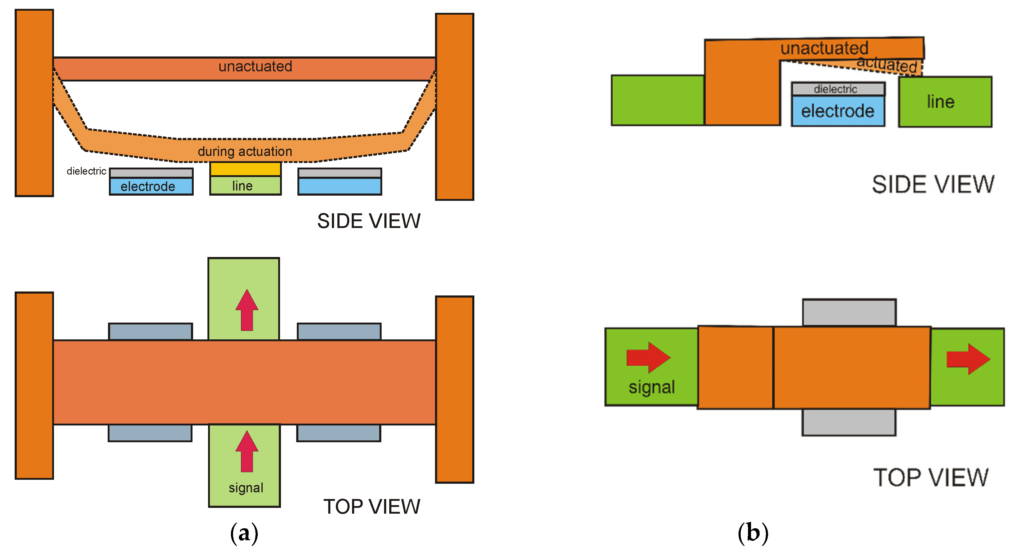
Electrical actuation of a microbeam is widely used in RF-MEMS switching devices. Electrically actuated switches are usually made of a conductive microbeam that can be either single or double clamped and one or more actuation electrodes below the beam, as illustrated in Figure 1. Their frequency application range goes from DC up to 30 GHz in the most frequent cases, but RF-MEMS switches purposely designed and fabricated on special substrates can reach frequencies up to 100 GHz.
Electrostatic actuation can be seen as a very useful instability. When the voltage applied to the actuation electrode gradually increases, the suspended beam bends progressively down, up to the point when the equilibrium between elastic and electrostatic forces cannot be maintained and the beam collapses on the electrode underneath, that is, it actuates [12]. In the case of a double-clamped beam, the actuation voltage of a rectangular beam is given by
where k is the spring constant of the beam, d is the distance between the suspended beam and the electrode, A is the electrode area, and ε0 is the vacuum permittivity.
When the voltage decreases after actuation has been reached, the beam bends up again, detaching from the electrode at a different potential, the release voltage, which is given by
and is always lower than the actuation voltage. In this case, d0 is the thickness of the dielectric layer above the electrodes and εr is its relative permittivity. More complex formulas can be derived for rectangular cantilever beams [13,14]. Complex beam geometries require simulation work in order to determine their actuation and release voltages, but in some special cases, useful approximate analytical formulas can be derived [2,15].
In an ideal device with a perfect dielectric, Vact and Vrel remain stable for an infinite time and after an infinite number of switching cycles. In the real world, instabilities and drift in both actuation and release voltages are fairly common and have different origins. The most frequent sources are charging of the dielectric, temperature variations, fabrication uncertainties, and material wear.
3. Instabilities Due to Dielectric Charging
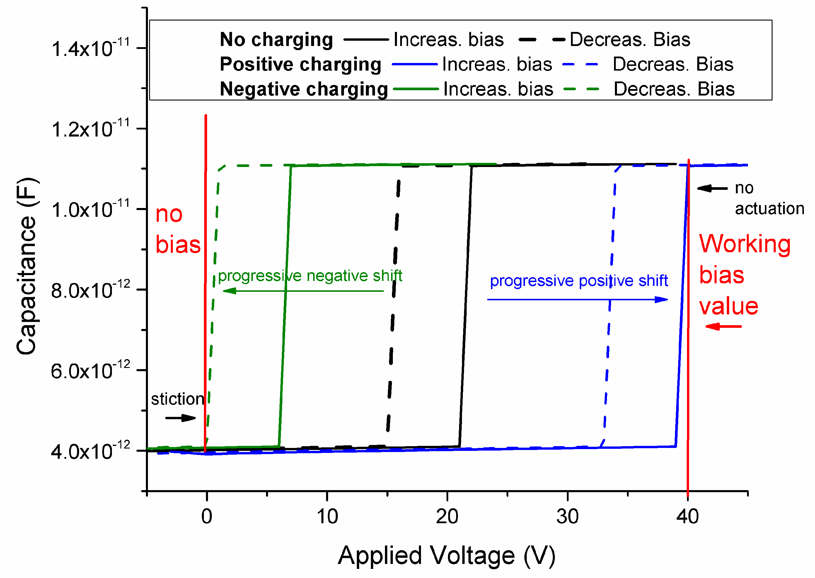
Dielectric charging has been widely studied in microswitching devices [16,17]. It is especially important in long-term actuation applications [18], but also plays a relevant role in many cycling experiments [19] because the effects of charging increase with time. The main effect of charging is a progressive drift of the release and actuation voltages, that can be either positive or negative and increases with bias time. The ultimate source of this problem is the presence of a dielectric between the bridge and the actuation electrodes, and it is therefore very important for capacitive switches [20]. Since a perfect dielectric does not exist, the real material becomes positively or negatively charged because of small defects in its structure, and this effect increases with actuation time. The effects of charging can generate several unwanted phenomena. The most important of these instabilities is caused by a progressive drift of the actuation and release voltages. Depending on the polarity applied and the nature of the charge traps, two different effects can be measured. In the first case, the release voltage drifts toward smaller values until it is so close to zero that the switch does not de-actuate anymore and remains stuck. In the second case, the actuation voltage can progressively increase to very high values until it is higher than the applied bias and the switch does not actuate. This behavior is schematically depicted in Figure 2. In real operation, stiction or actuation failure does not happen abruptly and without warning signs. In the first case, when the release voltage approaches zero, the adhesion forces between the surfaces can randomly prevent the release before the critical point, with a behavior that is largely unpredictable. In the other case, since charging phenomena are increased when the switch is actuated, and may slowly be reduced when the switch is de-actuated, an actuation voltage too close to the bias voltage can produce a continuous actuation-release mechanism not controlled by the external bias, which leads to a totally unstable switch.
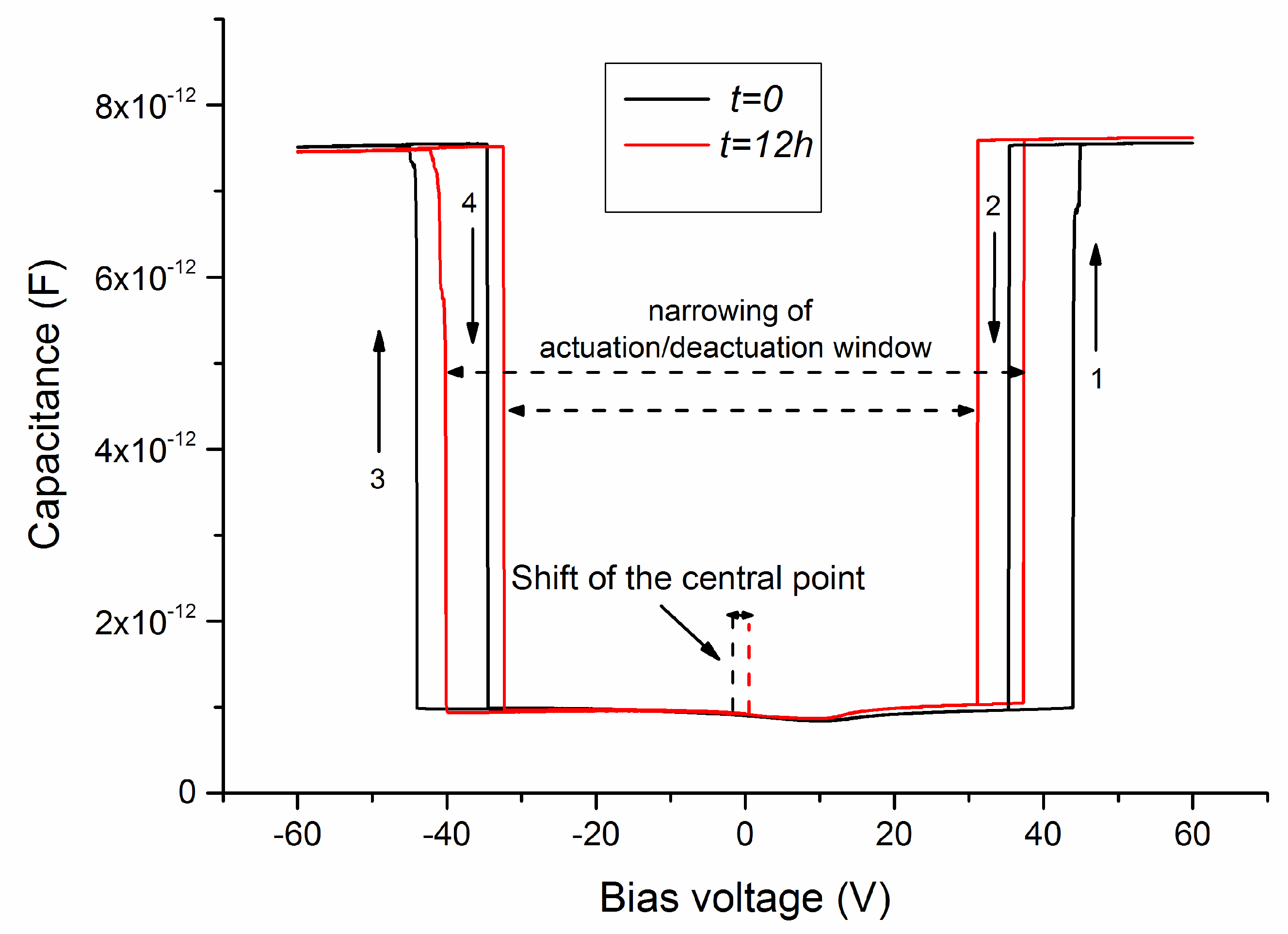
Different strategies have been developed to minimize charging phenomena either at material and design level or by applying specific voltage pulses [21]. The most promising ones work on the removal of the dielectric layer with the introduction of stopping pillars in order to avoid direct contact with the charged electrode [22]. These methods are quite effective and in fact, when most of the charge has been removed, other effects appear in the capacitance–voltage curve [23] evidencing complex charging effects either due to the inhomogeneous distribution of charge [24] or due to mechanical relaxation or creep [25,26]. In this case, a more complex model including both shifting and narrowing of the actuation/release curves must be applied to the experimental data in order to characterize the switch behavior, and the voltage scan must be bipolar in order to take into account the drift of both positive and negative values.
Unlike shift effects, narrowing effects in the capacitance–voltage curve are polarity independent and it is then quite hard to attribute them exclusively to dielectric charging. Shift and narrowing effects can be separated considering the average and the difference between the positive and negative actuation (and de-actuation) voltages [23,27]. The change in the average voltage is a measure of the narrowing, whereas the difference is a direct measure of the shift. A typical example of this behavior is reported in Figure 3, where a dielectric-less capacitive switch was biased above the actuation value for twelve hours. The measurements were performed by sweeping the applied voltage from 0 to 60 V and then from 60 to −60 V and finally from −60 to 0 V before and after biasing the switch at 60 V for 12 hours. The sweeping process lasted a few seconds.
4. Instabilities Due to Temperature Variations
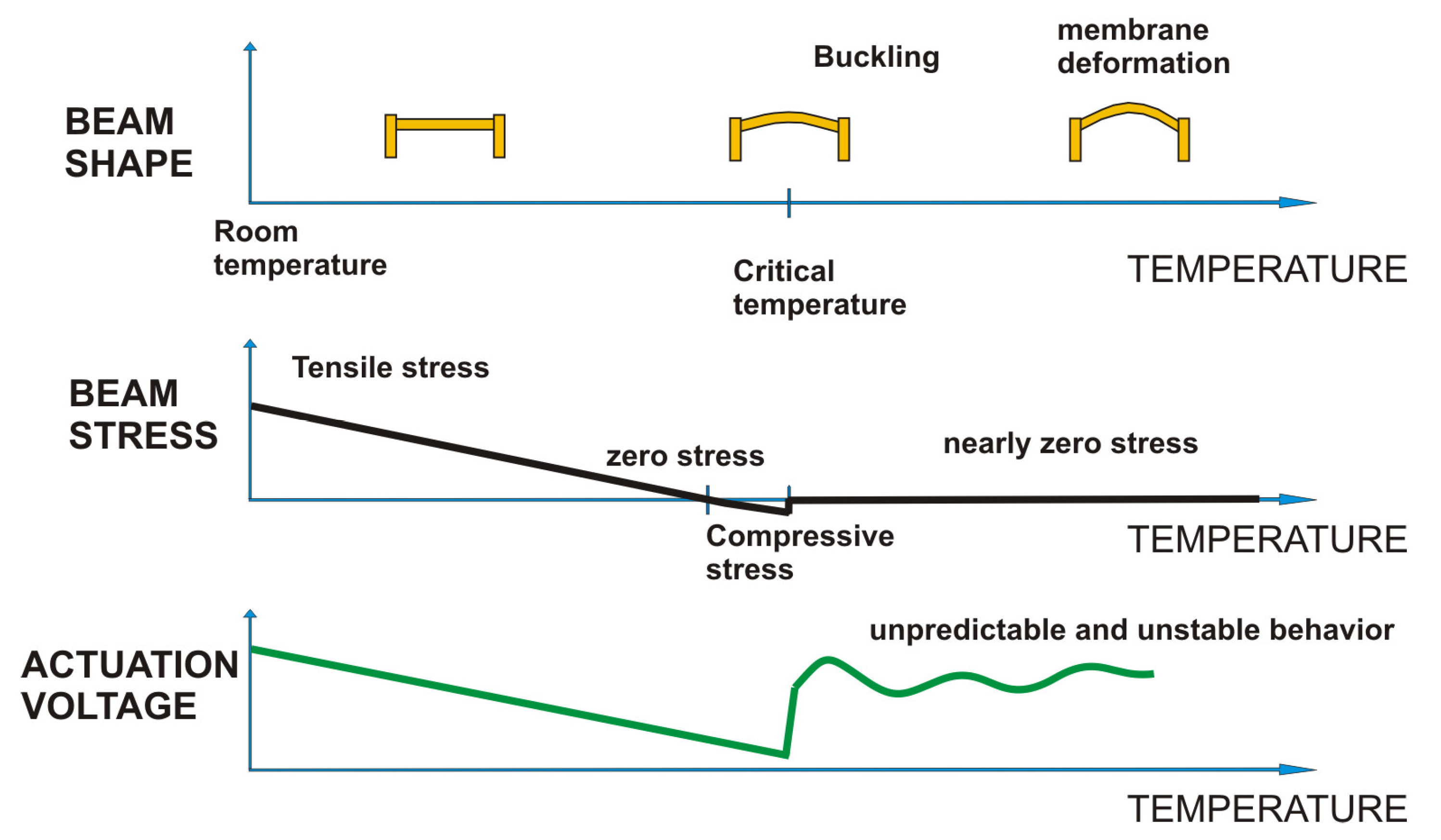
Variations of temperature are known to cause instability phenomena in suspended beams. The most important source of these instabilities is the difference in the linear thermal expansion (LTE) coefficient of the materials used for the suspended structure and the substrate. Switching beams are often made of metal, typically gold or aluminum, while the substrate is generally silicon or, for high-frequency switching, quartz. Both substrates have an LTE coefficient much lower than that of gold or aluminum. When the temperature rises, the beam expands more than the substrate. If the beam is a cantilever, this does not cause relevant effects on the geometry and the internal stress of the structure, because the beam is free to expand. Only minor changes in the switch parameters are expected in this case, due to the change in elastic modulus of the materials or stress gradient variations [28].
In the case of a double-clamped beam, the beam expansion is constrained by the supports and the beam experiences a compressive thermal stress which adds to the residual stress of the beam according to the following equation
where σtotal and σTamb are the beam’s total stress and residual stress at room temperature, E is the beam’s elastic modulus, ΔT is the temperature difference, and αbeam and αsubstrate are the LTE coefficients of the suspended beam and the substrate, respectively. The variations of beam shape, internal stress, and actuation voltage as a function of temperature are schematized in Figure 4.
When the temperature is high enough, the beam can no longer sustain the compression and buckles, assuming the typical out-of-plane curved shape. Buckling occurs when the temperature is higher than a threshold value, called the critical temperature [29]. The critical temperature depends on the geometry of the beam and on the room temperature residual stress of the beam, which is normally tensile. The more tensile the beam stress at room temperature, the higher the buckling temperature. However, the room temperature tensile stress is determined by the fabrication process conditions and is quite difficult to modify or control. Moreover, the higher the tensile stress, the higher the actuation voltage of the beam, since the stress influences its spring constant [25].
If we look at the actuation voltage variation with the temperature, we see that when the temperature increases, in the first phase the actuation and release voltages decrease, due to the reduction of the internal tensile stress. The actuation voltage reduction is roughly dependent on the square root of the temperature difference when the residual stress is high, as can be seen from Equation (4).
where kelastic(E) is the part of the spring constant which is stress independent and determined only by the elastic modulus E and B is a constant which depends on the beam geometry. A detailed analytical derivation of this formula is reported in [30].
When the internal stress is approximatively zero or slightly positive, the minimum actuation voltage is reached. After that, we enter the buckling zone, and the actuation becomes unstable and difficult to calculate. The reason for this instability is mainly mechanical. In order to minimize the internal compressive stress, the suspended membrane deforms in the out-of-plane direction and changes the value of the air gap, which is no longer a constant in Equations (1) and (2).
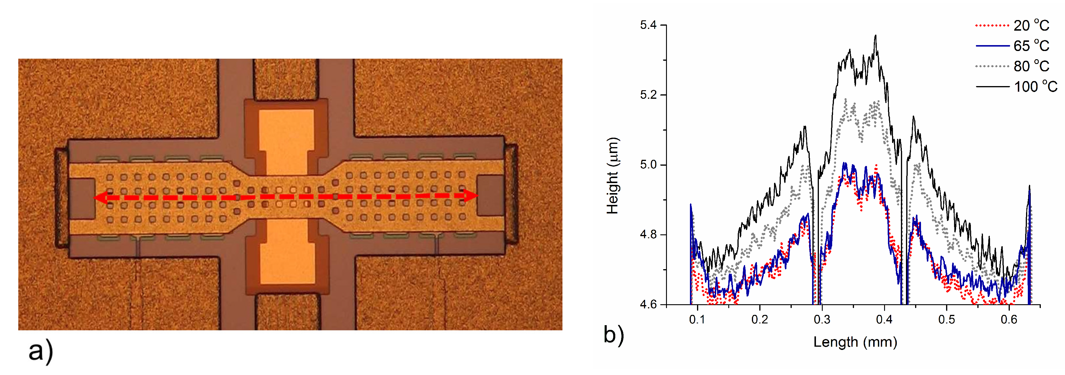
A real example of this behavior is reported in Figure 5, where a clamped–clamped capacitive switch with a gold suspended beam is measured with an optical profiler at different temperatures. From the figure, we see that the shape does not change until 65 °C and that the critical temperature is between 65 and 80 °C. The buckling is clearly evident at 80 °C and even more so at 100 °C. In fact, the non-perfect planarity of the membrane at 20 °C was due to thermal-stress-related processes in the release phase [31] at the end of the switch fabrication process.
The membrane shape above the critical temperature depends on its geometry and dimensions [28] and may vary several times while the temperature keeps increasing. In general, membrane anchors are the most important design detail in order to avoid unwanted deformations [32]. Anchoring systems that allow, at least partially, the lateral expansion of the membrane have a higher critical temperature and are less deformed by the temperature. In the example reported above, the actuation voltage was around 40 V at room temperature and around 20 V at the critical temperature (80 °C) [30].
5. Instabilities Due to Fabrication Uncertainties and Material Wear
When designing a device with suspended beams, an ideal fabrication process is normally assumed. In addition to that, design simplifying assumptions are often made, in order to reduce analytical modeling or simulation complexity.
The typical RF-MEMS capacitive switch consists of two actuating electrodes separated by a central underpass line where the signal travels, covered by a suspended movable beam clamped at both ends (see Figure 1a). This means that there are at least two actuation pads separated by the central line. In an ideal device, the beam is rigid and only the anchors bend when actuating. The electrodes and the line have the same height and the collapse on the electrodes occurs exactly when the beam contacts the dielectric above the line. Moreover, the effects of surface roughness are negligible.
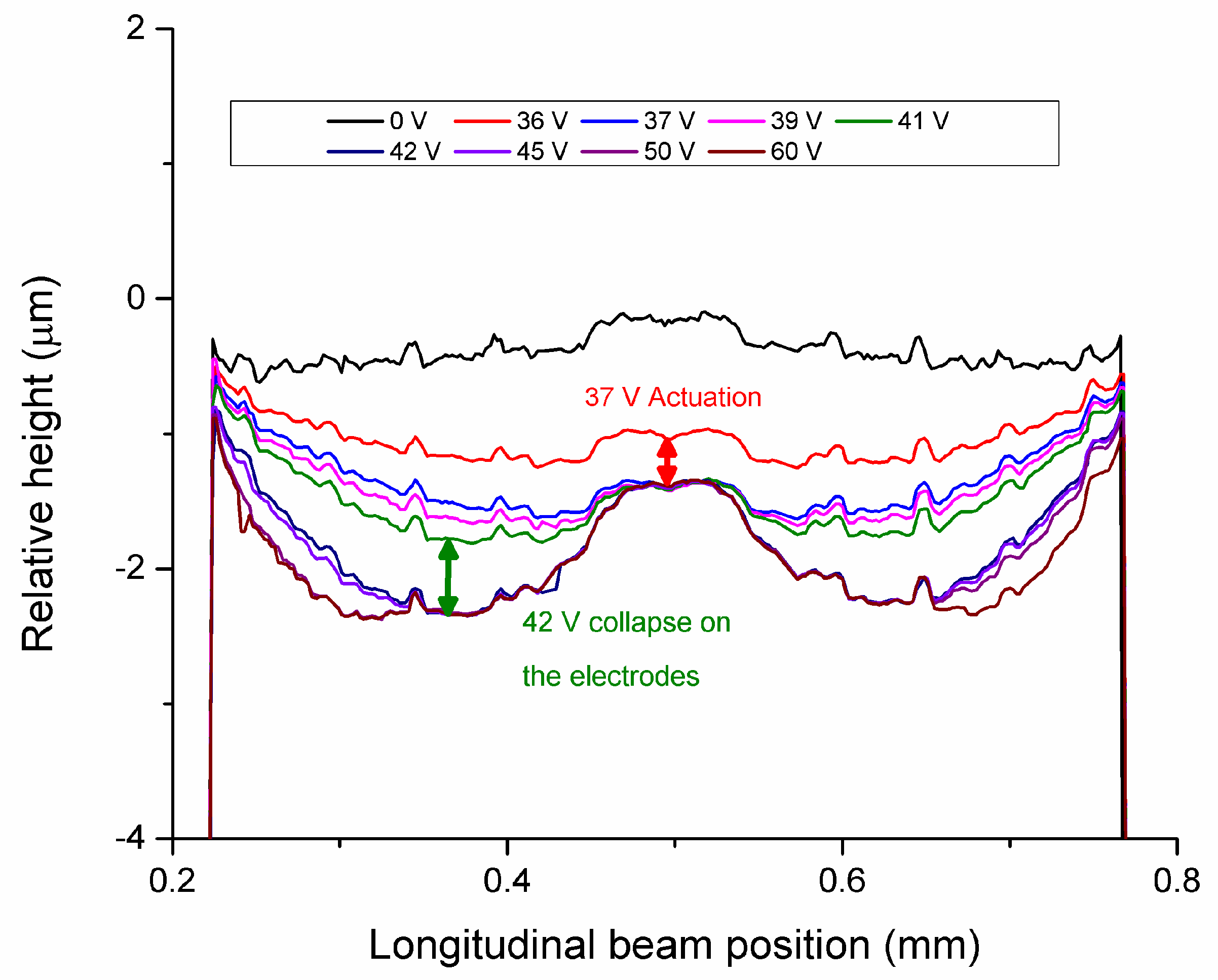
In a real device, the beam can be flexible, and the surface roughness can limit the contact surface between the membrane and the line [33,34]. Consequently, to assure a reliable actuation, the central line must be fabricated sensibly higher than the actuation electrode. This is especially true for dielectric-less switches with stopping pillars, a common design strategy aimed at reducing charging [22]. As a result, the line can be consistently higher than the actuation electrodes, with important consequences on the actuation and de-actuation properties of the switch. An example of this behavior is reported in Figure 6 for the same device depicted in Figure 5.
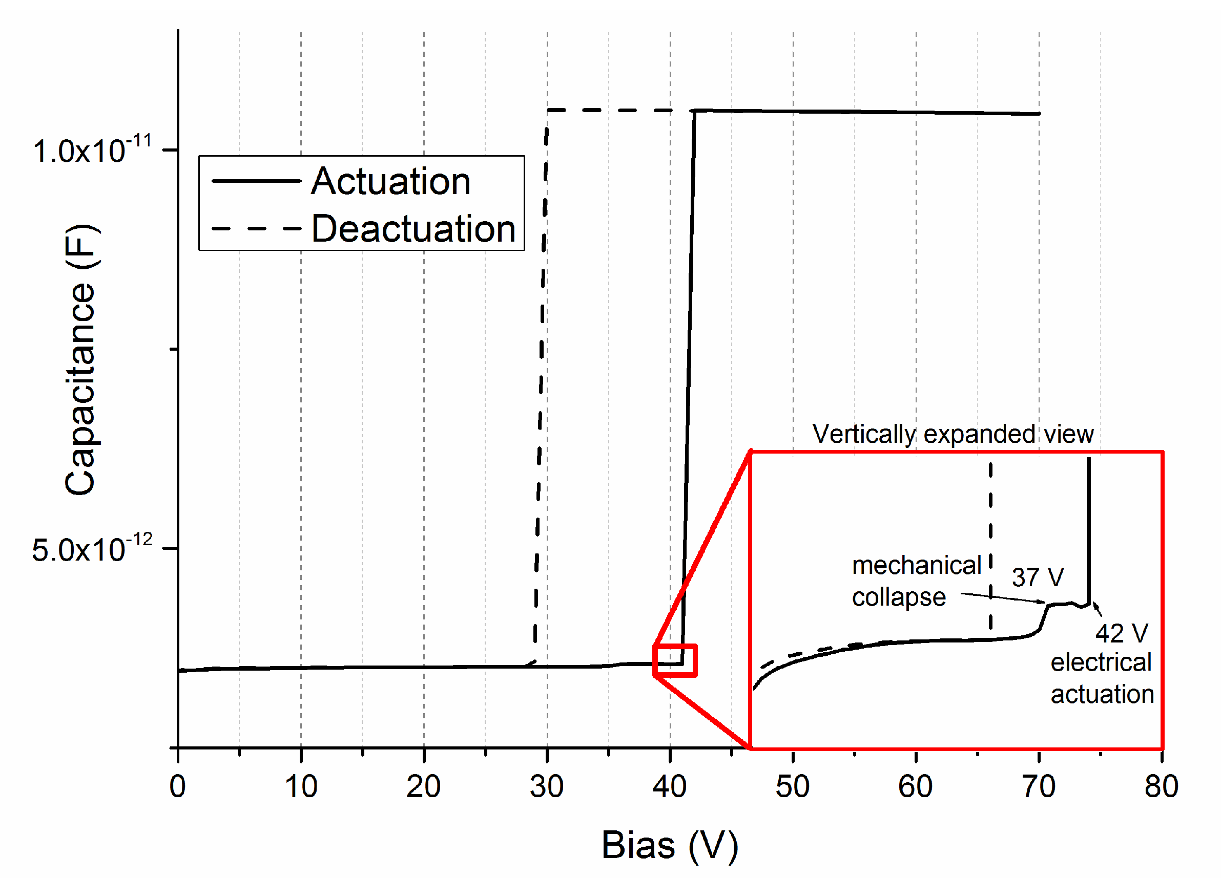
As can be seen from Figure 6, the switch presented not one but two collapse points as the applied bias increased. The first one was the actuation on the central line, which is the true mechanical actuation. The second one was the collapse on the actuation electrodes, and it usually happens a few volts after the first one. This double actuation was seen in the capacitance–voltage curve as a small “step”, as reported in the inset of Figure 7. As can be seen, mechanical and electrical actuation were 5 V apart in this case.
This behavior can be understood by taking into account the quality of the electrical contact. When dealing with microswitches, the quality of the contact is always an issue and is of paramount importance in the case of ohmic switches [35]. In MEMS devices, the contact forces are usually very low because of the small contact dimensions and a low contact force may result in a bad electric contact and bad switch performance. In the case reported above, after the first actuation, there is a poor electrical contact between the line and the beam. This happens because the contact force depends strongly on the height difference between the central line and the electrode [36]. For this reason, the second actuation where the beam collapses on the electrode is usually detected as an electrical actuation in the C–V curve. In this case, the contact force is much higher and the electrical contact is very good. On the other hand, this means that the experimental actuation voltage is normally higher than the simulated one by at least a few volts, depending on the switch geometry and on the flexibility of the membrane.
Unfortunately, the continuous actuation or a high number of switching cycles can also affect the quality of the electrical contact, which slowly degrades generating another type of performance drift and, eventually, another actuation failure. As the contact deteriorates, the difference of capacitance values in the on and off states becomes less sharply defined, and the RF performances deteriorate up to the point where it is not possible to clearly define an electrical actuation [37]. The quality of the contact [26] and the contact resistance vary randomly with time, and, again, the switch becomes highly unstable and therefore useless.
6. Conclusions
RF-MEMS switches are devices with suspended beams, intrinsically designed to be unstable. Instead of being a drawback, mechanical instability is exploited and controlled in order to switch between two electrical states that act differently on the signal line. However, in spite of the simplicity of this approach and the advantages in terms of performance, several unwanted conditions can lead to additional sources of drift and unstable behavior in these devices. The progress of research in the last decade has been very successful in preventing or minimizing these unwanted effects, especially with respect to the minimization and control of dielectric charging, but also in exploiting design solutions to increase the temperature stability and the long-term contact reliability. However, some concerns still prevent the complete elimination of reliability issues and, consequently, the full exploitation of these devices in commercial applications. Among them, some noteworthy concerns are the difficulties of an MEMS-compatible, hermetic, low-cost, wafer-level packaging, essential to avoid failure due to humidity or chemical contamination, and the scarcity of MEMS-specific methods for accelerated reliability testing. Nevertheless, some commercial RF-MEMS switches have appeared on the market and are gaining success for specific applications and uses, giving hope for the future.
Funding
This research received no external funding.
Conflicts of Interest
The author declares no conflict of interest.
References
- Senturia, S.D. Microsystem Design; Springer Science + Business Media: New York, NY, USA, 2001. [Google Scholar]
- Rebeiz, G.M. RF-MEMS: Theory, Design and Technology; John Wiley & Sons, Inc.: Hoboken, NJ, USA, 2004. [Google Scholar]
- Witvrouw, A.; Tilmans, H.A.C.; De Wolf, I. Materials issues in the processing, the operation and the reliability of MEMS. Microelectr. Eng. 2004, 76, 245–257. [Google Scholar] [CrossRef]
- Zhang, W.-M.; Yan, H.; Peng, Z.-K.; Meng, G. Electrostatic pull-in instability in MEMS/NEMS: A review. Sens. Actuators A Phys. 2014, 214, 187–218. [Google Scholar] [CrossRef]
- Sadeghian, H.; Yang, C.K.; Goosen, J.F.L.; van der Drift, E.; Bossche, A.; French, P.J.; van Keulen, F. Characterizing size-dependent effective elastic modulus of silicon nanocantilevers using electrostatic pull-in instability. Appl. Phys. Lett. 2009, 94, 221903. [Google Scholar] [CrossRef]
- Yao, J.J. RF MEMS from a device perspective. J. Micromech. Microeng. 2000, 10, R9–R38. [Google Scholar] [CrossRef]
- Daneshmand, M.; Mansour, R.R. Redundancy RF MEMS multiport switches and switch matrices. IEEE J. Microelectromech. Syst. 2007, 16, 296–303. [Google Scholar] [CrossRef]
- De Los Santos, H.J. RF MEMS Circuit Design for Wireless Communications; Artech House: Boston, MA, USA, 2002; ISBN 1-58053-329-9. [Google Scholar]
- Brown, E.R. RF-MEMS switches for reconfigurable integrated circuits. IEEE Trans. Microw. Theory Tech. 1998, 46, 1868–1880. [Google Scholar] [CrossRef]
- Shekhar, S.; Vinoy, K.J.; Ananthasuresh, G.K. Surface-micromachined capacitive RF switches with low actuation voltage and steady contact. J. Microelectromech. Systems 2017, 26, 643–652. [Google Scholar] [CrossRef]
- De Groot, W.A.; Webster, J.R.; Felnhofer, D.; Gusev, E.P. Review of device and reliability physics of dielectrics in electrostatically driven MEMS devices. IEEE Trans. Device Mater. Rel. 2009, 9, 90–202. [Google Scholar] [CrossRef]
- Tilmans, H.A.C. MEMS components for wireless communications. In Proceedings of the 16th European Conference on Solid-State Transducers (EUROSENSORS XVI), Prague, Czech Republic, 15–18 September 2002; pp. 1–34. [Google Scholar]
- Mulloni, V.; Resta, G.; Margesin, B. Clear evidence of mechanical deformation in RF-MEMS switches during prolonged actuation. J. Micromech. Microeng. 2014, 24, 075003. [Google Scholar] [CrossRef]
- Persano, A.; Iannacci, J.; Siciliano, P.; Quaranta, F. Out-of-plane deformation and pull-in voltage of cantilevers with residual stress gradient: Experiment and modelling. Microsyst. Technol. 2018. [Google Scholar] [CrossRef]
- Marcelli, R.; Lucibello, A.; De Angelis, G.; Proietti, E.; Comastri, D. Mechanical modelling of capacitive RF MEMS shunt switches. Microsyst. Technol. 2010, 16, 1057–1064. [Google Scholar] [CrossRef]
- Van Spengen, W.M. Capacitive RF MEMS switch dielectric charging and reliability: A critical review with recommendations. J. Micromech. Microeng. 2012, 22, 074001. [Google Scholar] [CrossRef]
- Papaioannou, G.; Papapolymerou, J.; Pons, P.; Plana, R. Dielectric charging in radio frequency microelectromechanical system capacitive switches: A study of material properties and device performance. Appl. Phys. Lett. 2007, 90, 233507. [Google Scholar] [CrossRef]
- Marcelli, R.; Papaioannou, G.; Catoni, S.; De Angelis, G.; Lucibello, A.; Proietti, E.; Margesin, B.; Giacomozzi, F.; Deborgies, F. Dielectric charging in microwave microelectromechanical Ohmic series and capacitive shunt switches. J. Appl. Phys. 2009, 105, 114514. [Google Scholar] [CrossRef]
- Goldsmith, C.; Ehmke, J.; Malczewski, A.; Pillans, B.; Eshelman, S.; Yao, Z.; Brank, J.; Eberly, M. Lifetime characterization of RF MEMS switches. In Proceedings of the 2001 IEEE MTT-S International Microwave Sympsoium Digest, Phoenix, AZ, USA, 20–24 May 2001; p. 227. [Google Scholar] [CrossRef]
- Lamhamdi, M.; Pons, P.; Zaghloul, U.; Boudou, L.; Coccetti, F.; Guastavino, J.; Segui, Y.; Papaioannou, G.; Plana, R. Voltage and temperature effect on dielectric charging for RF-MEMS capacitive switches reliability investigation. Microelectron. Reliab. 2008, 48, 1248–1252. [Google Scholar] [CrossRef]
- Peng, Z.; Yuan, X.; Hwang, J.C.M.; Forehand, D.I.; Goldsmith, C.L. Dielectric charging of RF MEMS capacitive switches under bipolar control-voltage waveforms. In Proceedings of the IEEE/MTT-S International Microwave Symposium, Honolulu, HI, USA, 3–8 June 2007. [Google Scholar] [CrossRef]
- Mardivirin, D.; Pothier, A.; Crunteanu, A.; Vialle, B.; Blondy, P. Charging in dielectricless capacitive RF-MEMS switches. IEEE Trans. Microwave Theory Tech. 2009, 57, 231–236. [Google Scholar] [CrossRef]
- Barbato, M.; Cester, A.; Mulloni, V.; Margesin, B.; Meneghesso, G. Transient evolution of mechanical and electrical effects in microelectromechanical switches subjected to long term stresses. IEEE Trans. Electron Devices 2015, 62, 3825–3831. [Google Scholar] [CrossRef]
- Rottenberg, X.; De Wolf, I.; Nauwelaers, B.K.J.C.; De Raedt, W.; Tilmans, H.A.C. Analytical model of the DC actuation of electrostatic MEMS devices with distributed dielectric charging and nonplanar electrodes. IEEE J. Microelectromech. Syst. 2007, 16, 1243–1253. [Google Scholar] [CrossRef]
- Mulloni, V.; Colpo, S.; Faes, A.; Margesin, B. A simple analytical method for residual stress measurement on suspended MEM structures using surface profilometry. J. Micromech. Microeng. 2013, 23, 025025. [Google Scholar] [CrossRef]
- Mulloni, V.; Solazzi, F.; Resta, G.; Giacomozzi, F.; Margesin, B. RF-MEMS switch design optimization for long-term reliability. Analog Integr. Circ. Sig. Process. 2014, 78, 323–332. [Google Scholar] [CrossRef]
- Mulloni, V.; Lorenzelli, L.; Margesin, B.; Barbato, M.; Meneghesso, G. Temperature as an accelerating factor for lifetime estimation of RF-MEMS switches. Microelectron. Eng. 2016, 160, 63–67. [Google Scholar] [CrossRef]
- Mulloni, V.; Sordo, G.; Margesin, B. An accelerated thermal cycling test for RF-MEMS switches. Microsyst. Technol. 2016, 22, 1585–1592. [Google Scholar] [CrossRef]
- Chen, K.-S. Techniques in Residual Stress Measurement for MEMS and Their Applications. In MEMS/NEMS Handbook—Techniques and Applications; Springer: Berlin, Germany, 2006; pp. 1252–1328. [Google Scholar]
- Mulloni, V.; Solazzi, F.; Ficorella, F.; Collini, A.; Margesin, B. Influence of temperature on the actuation voltage of RF-MEMS switches. Microelectron Reliab. 2013, 53, 706–711. [Google Scholar] [CrossRef]
- Mulloni, V.; Giacomozzi, F.; Margesin, B. Controlling stress and stress gradient during the release process in gold suspended micro-structures. Sens. Actuators A Phys. 2010, 162, 93–99. [Google Scholar] [CrossRef]
- Persano, A.; Quaranta, F.; Capoccia, G.; Proietti, E.; Lucibello, A.; Marcelli, R.; Bagolini, A.; Iannacci, J.; Taurino, A.; Siciliano, P. Influence of design and fabrication on RF performance of capacitive RF MEMS switches. Microsyst. Technol. 2016, 22, 1741–1746. [Google Scholar] [CrossRef]
- Yu, A.B.; Liu, A.Q.; Zhang, Q.X.; Hosseini, H.M. Effects of surface roughness on electromagnetic characteristics of capacitive switches. J. Micromech. Microeng. 2006, 16, 2157–2166. [Google Scholar] [CrossRef]
- Matrecano, M.; Memmolo, P.; Miccio, L.; Persano, A.; Quaranta, F.; Siciliano, P.; Ferraro, P. Improving holographic reconstruction by automatic Butterworth filtering for microelectromechanical systems characterization. Appl. Opt. 2015, 54, 3428–3432. [Google Scholar] [CrossRef]
- Sawant, V.B.; Mohite, S.S.; Cheulkar, L.N. Comprehensive contact material selection approach for RF MEMS switch. Mater. Today Proc. 2018, 5, 10704–10711. [Google Scholar] [CrossRef]
- Mulloni, V.; Resta, G.; Giacomozzi, F.; Margesin, B. Influence of fabrication tolerances on the reliability of RF-MEMS capacitive switches. In Proceedings of the 2015 XVIII AISEM Annual Conference, Trento, Italy, 3–5 February 2015; pp. 1–4. [Google Scholar] [CrossRef]
- Mulloni, V.; Barbato, M.; Meneghesso, G. Long-term lifetime prediction for RF-MEMS switches. J. Micromech. Microeng. 2016, 26, 74004–74012. [Google Scholar] [CrossRef]
Figure 1.
Typical clamped–clamped (a) and cantilever (b) switch configurations. Both configurations use mobile suspended beams as actuators.
Figure 1.
Typical clamped–clamped (a) and cantilever (b) switch configurations. Both configurations use mobile suspended beams as actuators.

Figure 2.
Scheme of capacitance–voltage (C–V) curves of a capacitive MEMS switch with charging phenomena. When the bias is applied, the actuation and release voltages can drift to higher values (positive charging) or lower values (negative charging).
Figure 2.
Scheme of capacitance–voltage (C–V) curves of a capacitive MEMS switch with charging phenomena. When the bias is applied, the actuation and release voltages can drift to higher values (positive charging) or lower values (negative charging).

Figure 3.
C–V curve of a dielectric-less capacitive switch before and after applying a positive bias at 60 V for 12 hours. Charging phenomena are strongly reduced (small shift of the central point) and narrowing effects become visible.
Figure 3.
C–V curve of a dielectric-less capacitive switch before and after applying a positive bias at 60 V for 12 hours. Charging phenomena are strongly reduced (small shift of the central point) and narrowing effects become visible.

Figure 4.
Scheme of the interrelation between temperature, beam shape, internal stress, and actuation voltage in a clamped–clamped beam. The precise value of the critical temperature depends on the beam’s geometry and material.
Figure 4.
Scheme of the interrelation between temperature, beam shape, internal stress, and actuation voltage in a clamped–clamped beam. The precise value of the critical temperature depends on the beam’s geometry and material.

Figure 5.
Micrograph (a) and surface profile (b) of the mobile membrane of a MEMS capacitive switch at different temperatures. The surface profile was measured with an optical profiler along the red dashed line (a).
Figure 5.
Micrograph (a) and surface profile (b) of the mobile membrane of a MEMS capacitive switch at different temperatures. The surface profile was measured with an optical profiler along the red dashed line (a).

Figure 6.
Evolution of the suspended beam shape at different (increasing) voltages for the RF-MEMS switch reported in Figure 5. The lines have been recorded with an optical profiler while biasing the switch.
Figure 6.
Evolution of the suspended beam shape at different (increasing) voltages for the RF-MEMS switch reported in Figure 5. The lines have been recorded with an optical profiler while biasing the switch.

Figure 7.
C–V curve of a capacitive MEMS switch. The inset reports the same curve expanded in the vertical direction. The first and the second collapse are clearly visible.
Figure 7.
C–V curve of a capacitive MEMS switch. The inset reports the same curve expanded in the vertical direction. The first and the second collapse are clearly visible.

© 2019 by the author. Licensee MDPI, Basel, Switzerland. This article is an open access article distributed under the terms and conditions of the Creative Commons Attribution (CC BY) license (http://creativecommons.org/licenses/by/4.0/).
Share and Cite
MDPI and ACS Style
Mulloni, V. Instability and Drift Phenomena in Switching RF-MEMS Microsystems. Actuators 2019, 8, 15. https://doi.org/10.3390/act8010015
AMA Style
Mulloni V. Instability and Drift Phenomena in Switching RF-MEMS Microsystems. Actuators. 2019; 8(1):15. https://doi.org/10.3390/act8010015
Chicago/Turabian StyleMulloni, Viviana. 2019. "Instability and Drift Phenomena in Switching RF-MEMS Microsystems" Actuators 8, no. 1: 15. https://doi.org/10.3390/act8010015
Note that from the first issue of 2016, this journal uses article numbers instead of page numbers. See further details here.