1. Introduction
Miniaturized ultrasensitive devices for medical point-of-care and industrial portable systems are in huge demand. Devices such as MEMS/NEMS mass sensors have rapidly evolved to a point that has enabled us to weigh single atoms with unparalleled precision [
1]. In order to widely deploy these devices for real-world consumer applications, comprehensive studies need to be performed to understand the technological limits of every design. The MEMS/NEMS devices have great potential for a broad spectrum of ultrasensitive mass sensing applications, such as label-free monitoring of biological interactions [
2], detection of gas molecules and volatile organic compounds [
3], thickness measurement of the deposited thin films, and so on. The working principle of this type of MEMS/NEMS resonant sensor is based upon measureable infinitesimal mechanical perturbation converted into the electrical domain via a variety of transduction mechanisms such as electrostatic, piezoelectric, and optical detection [
4]. Some of the most widely studied resonant mass sensors to date are quartz crystal microbalance (QCM), surface acoustic wave (SAW) resonators, and capacitively transduced NEMS/MEMS resonators [
5]. However, these technologies still face a number of challenges that limit their ultimate performance in mass sensing applications and seamless integration with CMOS IC technology including relatively low quality factors, low resonance frequencies, lack of scalability, need of vacuum environment, high motional resistance, and use of complex fabrication techniques [
6,
7,
8]. Lateral extensional mode ZnO-on-SOI MEMS resonators are an alternative and emerging technology that has promised a well-balanced solution to most of the aforementioned problems. These devices were initially developed for wireless transceivers because they have a great potential to satisfy the very stringent specifications of wireless communications standards such as low insertion loss, high frequency selectivity and low phase noise [
9].
Table 1.
Comparison of resonant sensing technologies evaluated by direct metal writing techniques.
Table 1.
Comparison of resonant sensing technologies evaluated by direct metal writing techniques.
| Device Type | Resonant Frequency (MHz) | Localized Mass Sensitivity (Hz·fg−1) | Mass Resolution (fg) (1 fg = 10−15 g) |
|---|
ZnO-on-Si Disk Resonator
(This work) | 85.4 | 1.17 | 0.367 |
| MEMS Cantilever [10] | 0.350 | 0.878 | N/A |
| Capacitive Disk Resonator [11] | 132 | 31.5 | 0.130 |
| Longitudinal Bulk Acoustic Resonator [12] | 51 | 100 | 0.5 |
| FBAR [13] | 2300 | N/A | 9 |
In the past few years, a great deal of effort has been devoted to study the performance characteristics of all the aforementioned resonant sensing technologies by using direct write techniques like focus ion beam (FIB) deposition, as well as other physical deposition techniques such as e-beam evaporation and sputtering. With these techniques, several research groups have reported the most important sensing parameters such as the mass sensitivity and resolution as summarized in
Table 1.
In this work, we present the sensitivity analysis of mass loading at both maximum and minimum displacement points of the fourth-order lateral-extensional mode of a ZnO-on-SOI disk resonator. The devices have been fabricated on a silicon-on-insulator (SOI) wafer by using a recently developed 5-photomask CMOS compatible batch microfabrication process [
14]. In particular, ten piezoelectrically-transduced 40 μm-radius ZnO-on-SOI disk resonators operating in the fourth-order contour mode have exhibited resonance frequencies of roughly 86 MHz with measured Q factors exceeding 6000 (in air) and 10,000 (in vacuum). Three of the devices have been tested as mass sensors which demonstrated a sensitivity of 1.17 Hz·fg
−1 and 0.334 Hz·fg
−1 (1 fg = 10
−15 g) induced by the loaded mass at the maximum and minimum displacement points accordingly. Aside from the reduced sensitivity, it is observed that the loaded mass on the nodal points also leads to significant Q-factor degradation, which greatly affects the overall performance of the device in terms of increased motional impedance and lowered resolution. On the contrary, the loaded mass on the maximum displacement locations has led to much more repeatable and linear mass sensitivity and with less than 33.3 ppm of deviation in term of mass-loading induced fractional frequency change. The systematic investigation of the localized mass loading effect by this work is expected to expand our knowledge base and greatly improve our understanding of the behavior of the resonant mass sensor while providing crucial design criteria for the implementation of binding sites for optimum sensor performance.
2. Design and Operation
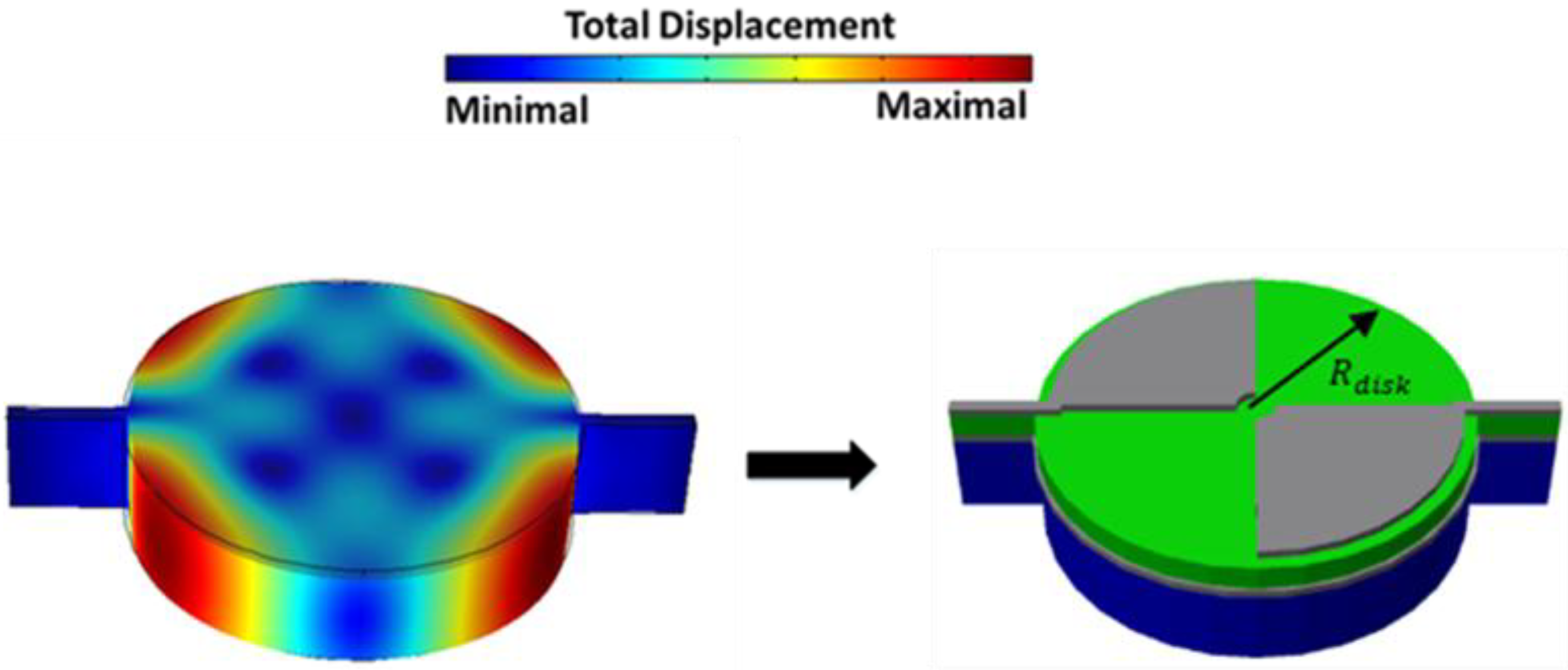
The ZnO-on-SOI lateral-extensional mode resonator was equipped with two split top electrodes in order to match the strain field patterns of the fundamental and the fourth-order extensional contour modes while operating in a 2-port configuration as seen in
Figure 1. When the added infinitesimal mass is much smaller than the device’s equivalent dynamic mass at the corresponding location, the mass sensitivity of the device can be related to the induced frequency shift, which is proportion to the ratio between the mode frequency and the equivalent mass given by:
where
is the measurable resonance frequency shift,
is the change due to the loaded mass,
is the resonance frequency of the fourth-order contour mode and
is the equivalent dynamic mass of the resonator at the attachment location of the loaded mass. It is worthwhile mentioning that the fourth-order contour mode of the device was employed because it offers the highest frequency-Q product for this electrode and anchor configuration for disk resonators with radius smaller than 100 µm. A shown in
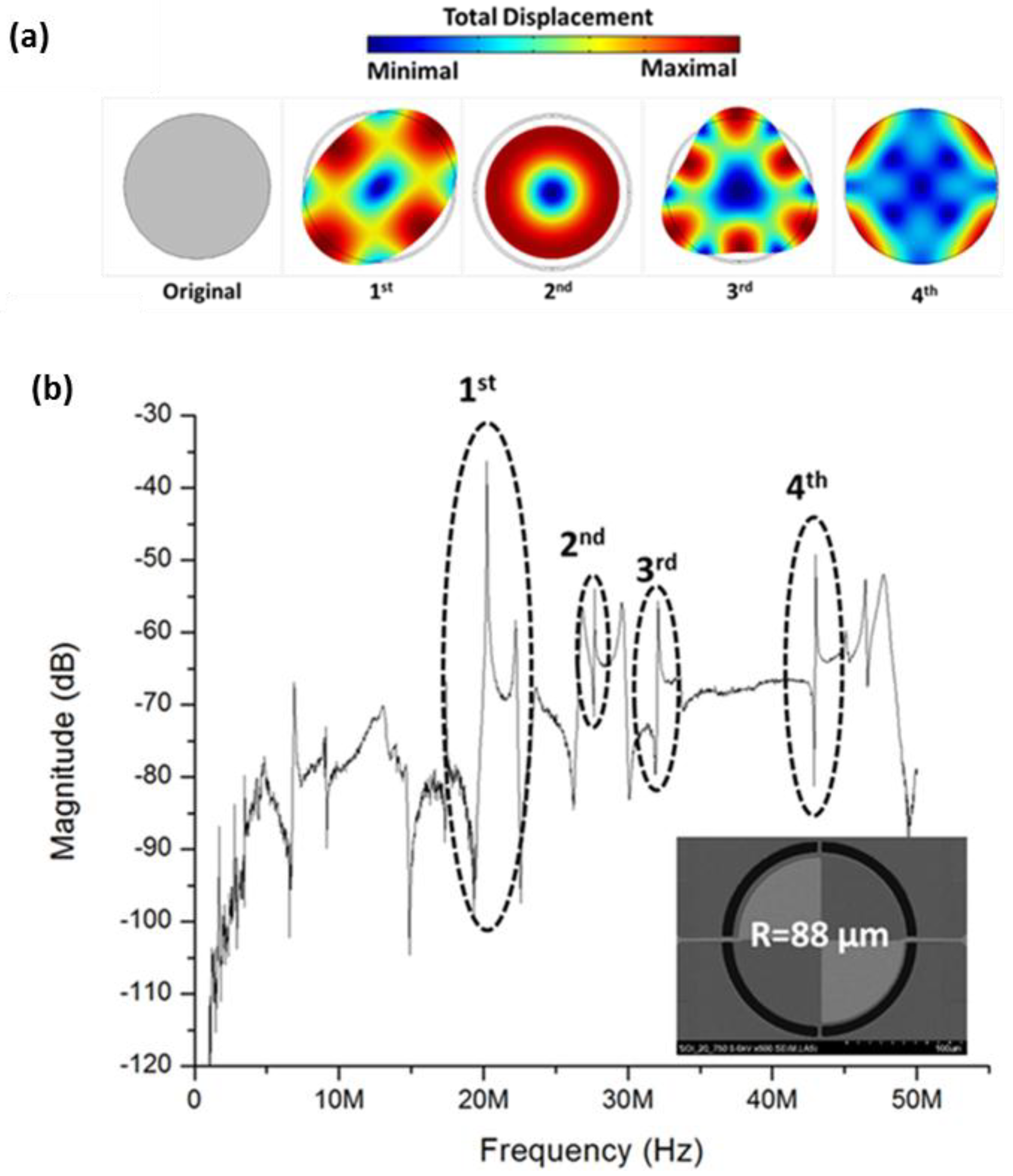
Figure 2a,b, only two resonant modes can be efficiently actuated based on the electrode and disk resonator mode shape design, which are the first-order and the fourth-order contour modes. As shown in
Figure 1, the correlations between the electrode shape, size of the resonant body and the position of the anchors
versus the modal strain fields strongly influence the electromechanical coupling and the anchor-related energy dissipation, the fourth-order contour resonant mode is anticipated to provide the highest frequency-Q product. As shown in
Figure 2b, the first four contour modes are identified for a 88 µm-radius disk resonator from its measured wideband frequency response with frequency range spanning from 30 kHz to 50 MHz. The resonant characteristics of these contour modes were explored by COMSOL® modal simulation using an equivalent acoustic velocity
found from Equation (3) for the ZnO-on-SOI disk resonator. As seen in
Table 2, the simulated resonant frequencies for the first four contour modes of a 88 μm-radius disk resonator match closely with the measured values, which verifies their coexistence and superior frequency-Q product of the fourth contour mode studied by this work. For the resonant mass sensor application, which monitor mass-loading induced frequency shift, both high frequency and high Q can be leveraged to achieve high sensitivity and high resolution simultaneously. The required radius for the disk resonator for the desired resonance frequency at this corresponding 4th order contour mode can be obtained by [
15]:
where
is the frequency scaling factor related to the fourth-order resonant mode (
= 0.493),
is the radius of the resonator disk and
is the equivalent acoustic velocity. For the ZnO-on-SOI resonator made of stacked structural layers, the equivalent acoustic velocity
can be expressed as:
where
,
,
,
are the equivalent Young’s modulus, density, Poisson’s ratio and the thickness of the corresponding layer of the stacked structural materials, including top/bottom metal electrode layer, ZnO piezoelectric transducer layer and silicon device layer.
Figure 1.
Split top electrode design mapping the resonant mode shape to maximize the output response generated by the ZnO piezoelectric transducer layer for a fourth-order contour resonant mode.
Figure 1.
Split top electrode design mapping the resonant mode shape to maximize the output response generated by the ZnO piezoelectric transducer layer for a fourth-order contour resonant mode.
Table 2.
Measured vs. simulated resonant characteristics of the first four contour modes of a 88 µm-radius disk resonator device.
Table 2.
Measured vs. simulated resonant characteristics of the first four contour modes of a 88 µm-radius disk resonator device.
| Resonant Mode | Measured In-Air Q-Factor | Measured Resonant Frequency (MHz) | Simulated Resonant Frequency (MHz) |
|---|
| 1st | 2011 | 20.24 | 22.10 |
| 2nd | 1103 | 27.65 | 27.79 |
| 3rd | 462 | 32.10 | 33.97 |
| 4th | 3788 | 42.97 | 40.07 |
Figure 2.
(a) COMSOL® finite element eigenfrequency simulation demonstrating the first four extensional contour modes of a disk resonator; and (b) a measured wide-band forward transmission frequency response of a 88 µm-radius disk resonator with frequency range spanning from 30 kHz to 50 MHz.
Figure 2.
(a) COMSOL® finite element eigenfrequency simulation demonstrating the first four extensional contour modes of a disk resonator; and (b) a measured wide-band forward transmission frequency response of a 88 µm-radius disk resonator with frequency range spanning from 30 kHz to 50 MHz.
It is important to note that the equivalent dynamic mass of the resonator body tends to be much smaller than its physical mass, as different infinitesimal elements contribute based on the level of their kinetic energies. In another word, the regions adjacent to the nodal locations make significantly smaller contributions as compared to those of maximum displacement areas. Hence, the equivalent dynamic mass of the disk-shaped resonator body can be approximated by dividing its total kinetic energy by one-half of the square velocity at a specific circumferential location given by [
16]:
where
is the Bessel function of the first kind,
Rdisk is the radius of the resonator disk,
is the forth-order angular resonant frequency.
The equivalent stiffness of the resonator can be determined by:
As the device goes into resonance in a 2-port configuration, the electromechanical coupling efficiency between the electrical and acoustic energies at the terminals of the two split top electrodes can be calculated by the total charge induced through the piezoelectric effects underneath the electrodes at the maximum displacement region. The electromechanical coupling coefficient can be expressed as:
where
is the transverse piezoelectric strain coefficient, which equals to −4.7 pC/N for sputtered ZnO thin films [
17].
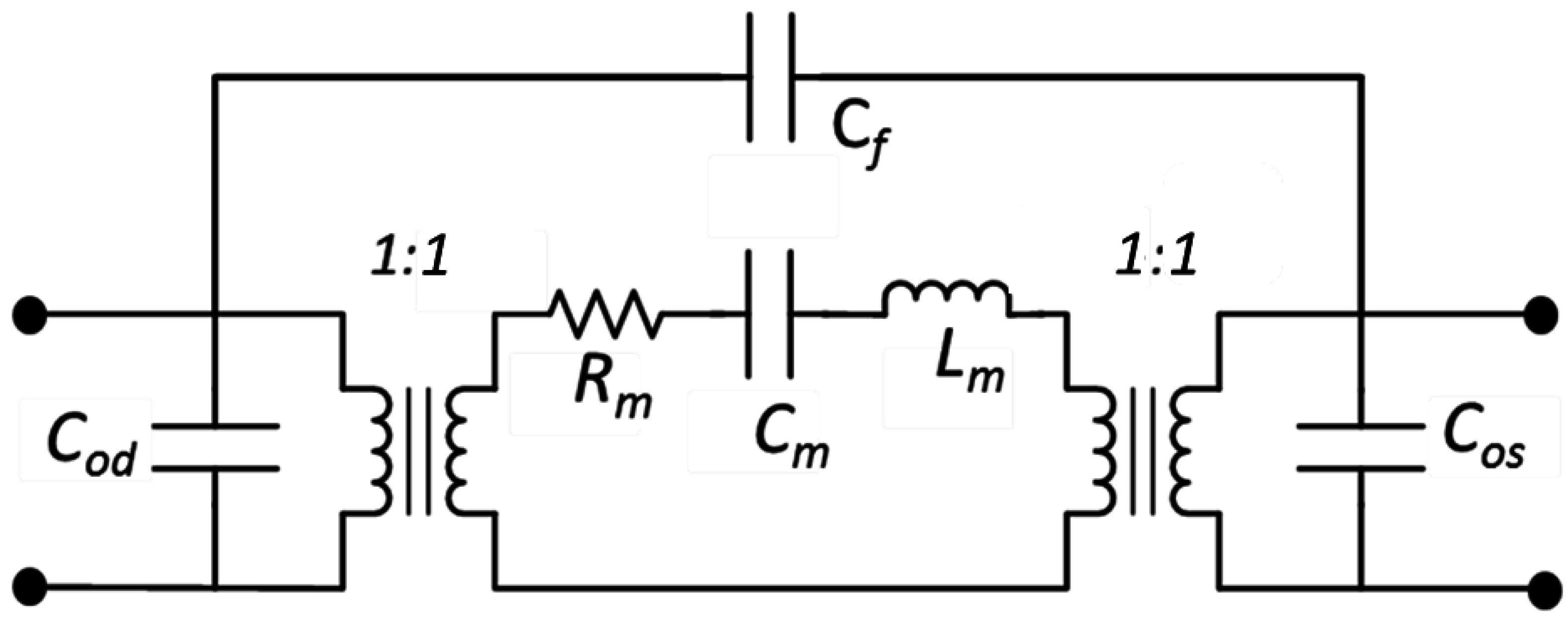
Figure 3.
The lumped-element equivalent circuit model of a 2-port ZnO-on-SOI resonator.
Figure 3.
The lumped-element equivalent circuit model of a 2-port ZnO-on-SOI resonator.
In order to model the behavior of a two-port piezoelectrically-transduced MEMS disk resonator, a lumped element circuit model as shown in
Figure 3 is employed with all the crucial parameters extracted from the measured characteristics. The two transformers represent electromechanical signal conversion by the piezoelectric transducers at the input and output ports, while the capacitors
Cod and
Cos represent the static stray capacitances of the driving and sensing electrodes. The series LCR electrical equivalent circuit can be derived from the corresponding mechanical model elements (
i.e., stiffness, mass, damping) using Equations (7)–(9) to depict the frequency-domain mechanical resonance behavior of the resonating body. The substrate feedthrough capacitance C
f accounts for the RF signal leakage between the input and output electrodes through the piezoelectric transducer layer and the resonator body.
The element values of the lumped-element LCR equivalent circuit can be expressed as follow:
where
mre,
Kre represent the equivalent mass, equivalent stiffness, and unloaded quality factor at the fourth-order resonant mode, respectively. The electromechanical coupling coefficient,
ηre, represents the energy conversion efficiency between the electrical and mechanical domains at both input and output terminals of the two-port resonator device.
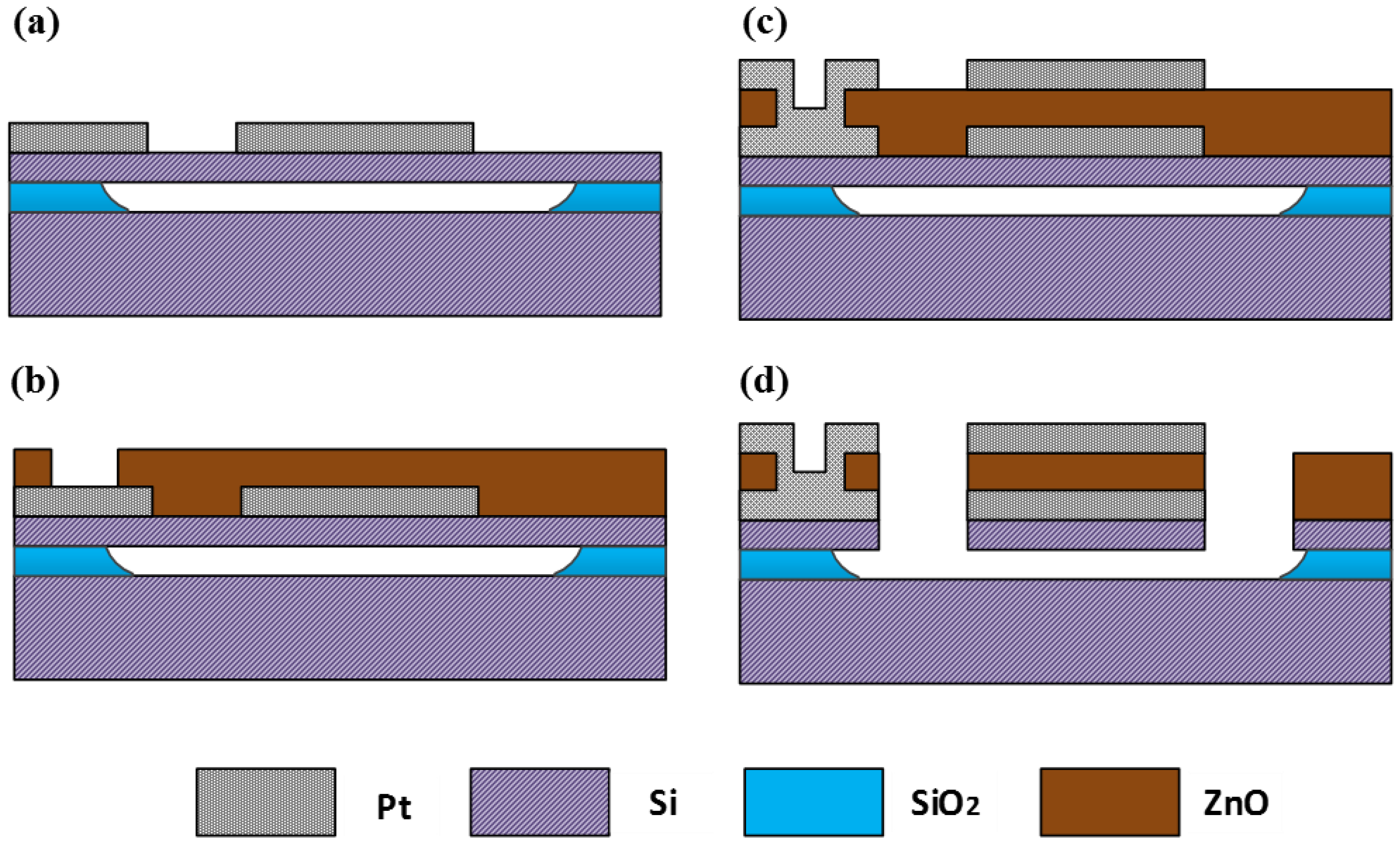
Device Microfabrication Processes
The sensors of this work were microfabricated through a five UV photo-mask process, starting with a SOI wafer with a highly doped 20 μm-thick silicon device layer, by using the cleanroom facility of the Nanotechnology Research and Education Center (NREC) at the University of South Florida.
Figure 4.
(a) A pre-releasing step followed by pattering of the bottom electrodes by lift-off process; (b) deposition of ZnO as the piezoelectric transducer layer; (c) patterning of via-hole contacts and the top electrodes; (d) defining the body of the resonator by a sequential ZnO RIE and Si DRIE processes.
The process begins with a pre-releasing step by using a 49% HF solution to undercut the device regions through strategically placed release holes, which were defined by dry etching through the silicon device layer. Then, the 200 nm-thick platinum bottom electrodes are deposited and patterned by lift-off as shown in
Figure 4a, followed by the reactive sputtering of a 500 nm-thick c-axis aligned ZnO film using a AJA Orion 5 magnetron RF sputtering system (
Figure 4b). The sputtering process parameters of ZnO thin films have been optimized to obtain a strong preferential c-axis orientation along the film normal direction (002) along with increased deposition rate of ~250 nm/h.
In situ post-process annealing at 400 °C has been performed for 1 h with Ar:O
2 (1:1) forming gases at 30 mTorr of pressure under a vacuum environment. The via-hole contacts to the bottom electrodes are subsequently opened by a wet chemical etching of ZnO in a mixture of 1:100 HCl:H
2O, followed by sputter deposition and lift-off patterning of the 200 nm-thick platinum top electrodes (
Figure 4c). Thereafter, the body of the resonator is then defined by a sequential reactive ion etching (RIE) and deep reactive ion etching (DRIE) of stacked ZnO and silicon device layers (
Figure 4d). The devices are then protected with a layer of photoresist and diced into individual chips. Finally, the batch-fabricated devices are released by a sequential acetone and methanol solvent rinsing followed by critical CO
2 drying.
Table 3.
Measured frequency characteristics of ten disk resonator devices operating at the fourth-order contour mode, which all have a 40 μm radius, 20 μm-thick silicon device layer and 5 μm-long supporting anchors but different anchor numbers and widths.
Table 3.
Measured frequency characteristics of ten disk resonator devices operating at the fourth-order contour mode, which all have a 40 μm radius, 20 μm-thick silicon device layer and 5 μm-long supporting anchors but different anchor numbers and widths.
| Device | Resonant Frequency (MHz) | Measured Q Factor (in Air) | Number of Anchors | Width of Anchors (µm) |
|---|
| 1 | 86.50155 | 7036 | 2 | 3 |
| 2 | 86.18316 | 6393 | 2 | 4 |
| 3 | 86.45038 | 6599 | 4 | 4 |
| 4 | 86.49768 | 6518 | 4 | 5 |
| 5 | 86.50036 | 7107 | 4 | 3 |
| 6 | 86.76068 | 6941 | 4 | 4 |
| 7 | 84.99902 | 6364 | 2 | 5 |
| 8 | 85.14952 | 6245 | 2 | 6 |
| 9 | 84.88901 | 7081 | 2 | 5 |
| 10 | 85.38877 | 6557 | 2 | 6 |
The measured results of ten 40 μm-radius disk resonator devices operating at the fourth-order contour mode under ambient conditions are shown in
Table 3. We can observe that there is a small variation of the loaded Q factors and the resonant frequencies partially due to discrepancies of thin-film depositions and UV contact photolithography. Specifically, physical vapor deposition systems such as the e-beam evaporator and sputtering systems used in this work tend to have limited thickness uniformity throughout a 10 cm diameter substrate. Similarly, the lamp of UV contact lithographic exposure systems lamps often produce a light intensity with limited uniformity thus causing geometry variation across different areas of the wafer. Despite the limited fabrication tolerance of a university cleanroom facility, the yield of these devices is greater than 90% and the variations of resonant frequency and loaded Q factor among ten measured devices are less than 1.9 MHz and 1000, respectively. It is worth mentioning that these devices have different numbers of supporting anchors strategically positioned at nodal points together with their anchor width ranging from 3 μm to 6 μm. Even though the radius of the resonator body plays a paramount role in setting the resonance frequency, a fraction of the observed variations of frequencies and Q factors amongst these devices can be ascribed to the differences in anchor sizes and numbers.
3. Results and Discussion
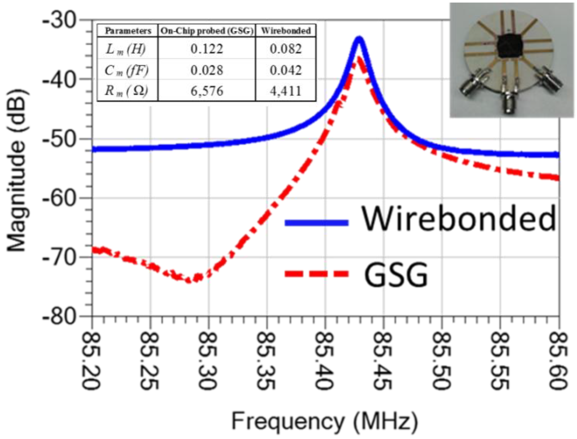
After the initial on-wafer probing test, the diced chip was then mounted onto a printed circuit board (PCB) chip carrier while the device under test was connected to the external ports using a ball wire bonder. The device was tested and the electrical parameters were obtained as shown in
Figure 5. As shown, the anti-resonance peak observed by the two port ground-signal-ground (GSG) on-wafer probing measurement is mitigated by the extra parasitics introduced by the PCB chip carrier and wire bonds. Using the lumped-element equivalent circuit model as shown in
Figure 3, the element values of the LCR electrical characteristics based on the on-chip probed and wire-bonded measurements were obtained as seen in the indented table in
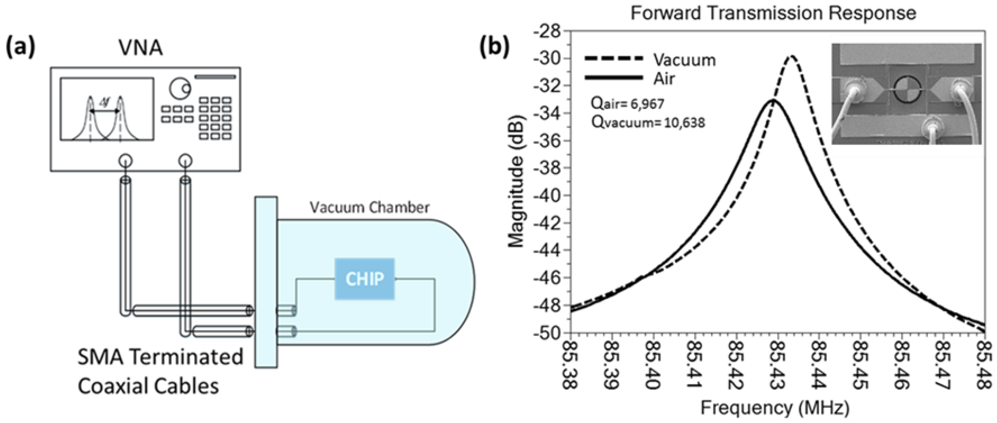
Figure 5. The device was then tested inside a vacuum chamber to provide a controlled environment (
Figure 6a).
The frequency responses of the devices were captured in the form of S-parameters using a vector network analyzer. As shown in
Figure 6b, the device has exhibited a resonant frequency of 85.4 MHz and a loaded Q factor of 6967 and 10,638 in air and in vacuum, respectively. The measured sensitivity of this device is 1.17 Hz·fg
−1 in response to the loaded mass at its maximum displacement locations, which is on par with the theoretically extrapolated value of 1.379 Hz·fg
−1 for a model-predicted equivalent dynamic mass
of 31.1 ng based on Equation (3). The same device has exhibited more than 3X lower mass-loading sensitivity of 0.334 Hz·fg
−1 at the minimum displacement locations adjacent to the nodal points. The sensitivity and effects of mass loading
versus modal location on the surface of the contour mode resonator were thoroughly explored through a series of depositions that lead to well-controlled infinitesimal increment of the loaded mass at the maximum and minimum displacement locations.
Figure 5.
Frequency responses of a fourth-order contour-mode disk resonator measured using an on-chip ground-signal-ground (GSG) probing and a PCB chip carrier with bond wires.
Figure 5.
Frequency responses of a fourth-order contour-mode disk resonator measured using an on-chip ground-signal-ground (GSG) probing and a PCB chip carrier with bond wires.
In this work, depositions of micro-pellets composed of platinum-gallium alloy composite were performed on predetermined areas (i.e., maximum or minimum displacement locations) using a Quanta 200 3D dual beam focused ion beam (FIB) equipped with a Gas Injection System (GIS).
Figure 6.
(a) Schematic diagram of the custom-built vacuum chamber test set-up used to characterize the resonant mass sensors under controlled environment; and (b) measured frequency responses of the ZnO-on-SOI resonator in both vacuum and air.
Figure 6.
(a) Schematic diagram of the custom-built vacuum chamber test set-up used to characterize the resonant mass sensors under controlled environment; and (b) measured frequency responses of the ZnO-on-SOI resonator in both vacuum and air.
The FIB platinum-gallium deposition process was calibrated until repeatable micro-pellets were obtained by using a low beam current of 10 pA to mitigate the gallium contamination as shown in
Figure 7b. It is important to note that even after a thorough calibration, the sizes, shapes and compositions of micro-pellets formed by FIB tend to vary slightly due to the change in FIB chamber conditions, which is a source of uncertainty for the mass sensitivity characterization in this work.
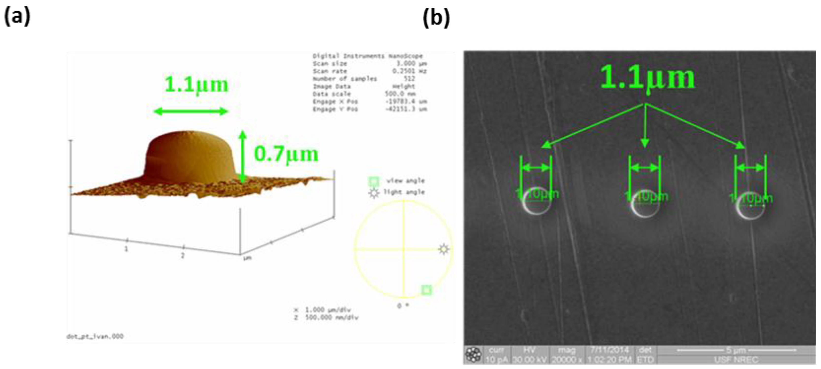
Figure 7.
(a) A high-resolution AFM scan of FIB deposited Pt/Ga micro-pellet; (b) a high-resolution SEM image multiple FIB micro-pellets showing great repeatability and fabrication tolerance.
Figure 7.
(a) A high-resolution AFM scan of FIB deposited Pt/Ga micro-pellet; (b) a high-resolution SEM image multiple FIB micro-pellets showing great repeatability and fabrication tolerance.
By using C
5H
5Pt(CH
3)
3 as an organometallic precursor, the typical FIB deposition leads to a micro-pellet that consists of C (45%–55%), O (5%), Pt (40%–50%), and Ga (5%–7%) [
18]. As shown in
Figure 7a, the FIB deposited micro-pellets were characterized using a high-resolution atomic force microscope (AFM), which revealed a nominal volume of 0.665 μm
3 corresponding to 7 pg of effective mass based on the PT/Ga alloy density of 10.2 g·cm
−3.
As shown in
Figure 8a, four consecutive micro-pellet depositions were performed to produce a discrete increment of 7 pg per micro-pellet as the extra loaded mass at the maximum displacement points near the disk circumference, which yield an average mass sensitivity of 1.17 Hz·fg
−1. To minimize the disturbance of the lateral external mode by the mass-loading effect, the micro-pellets were added one by one on the opposite sides of the disk resonator to retain the balance.
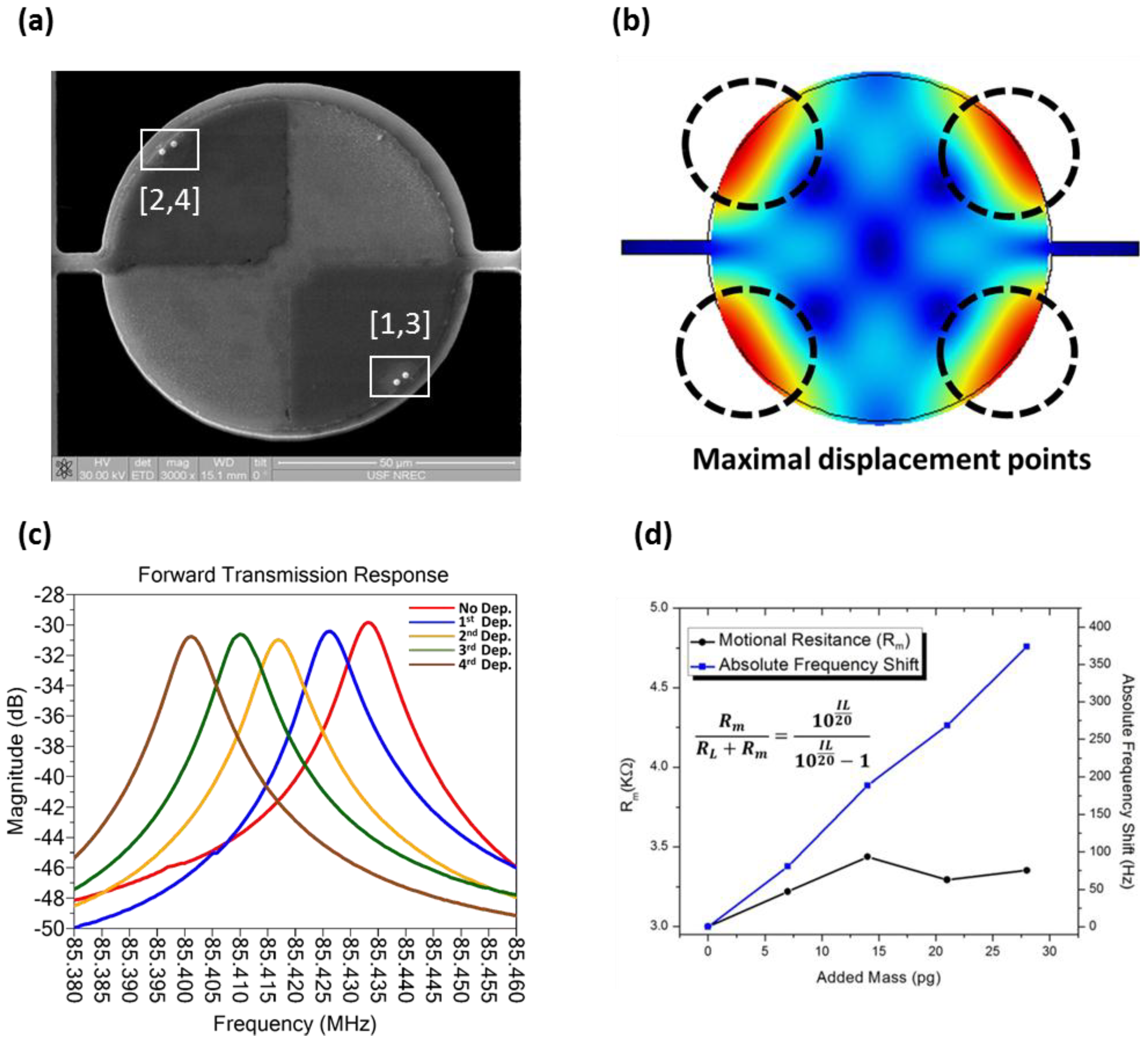
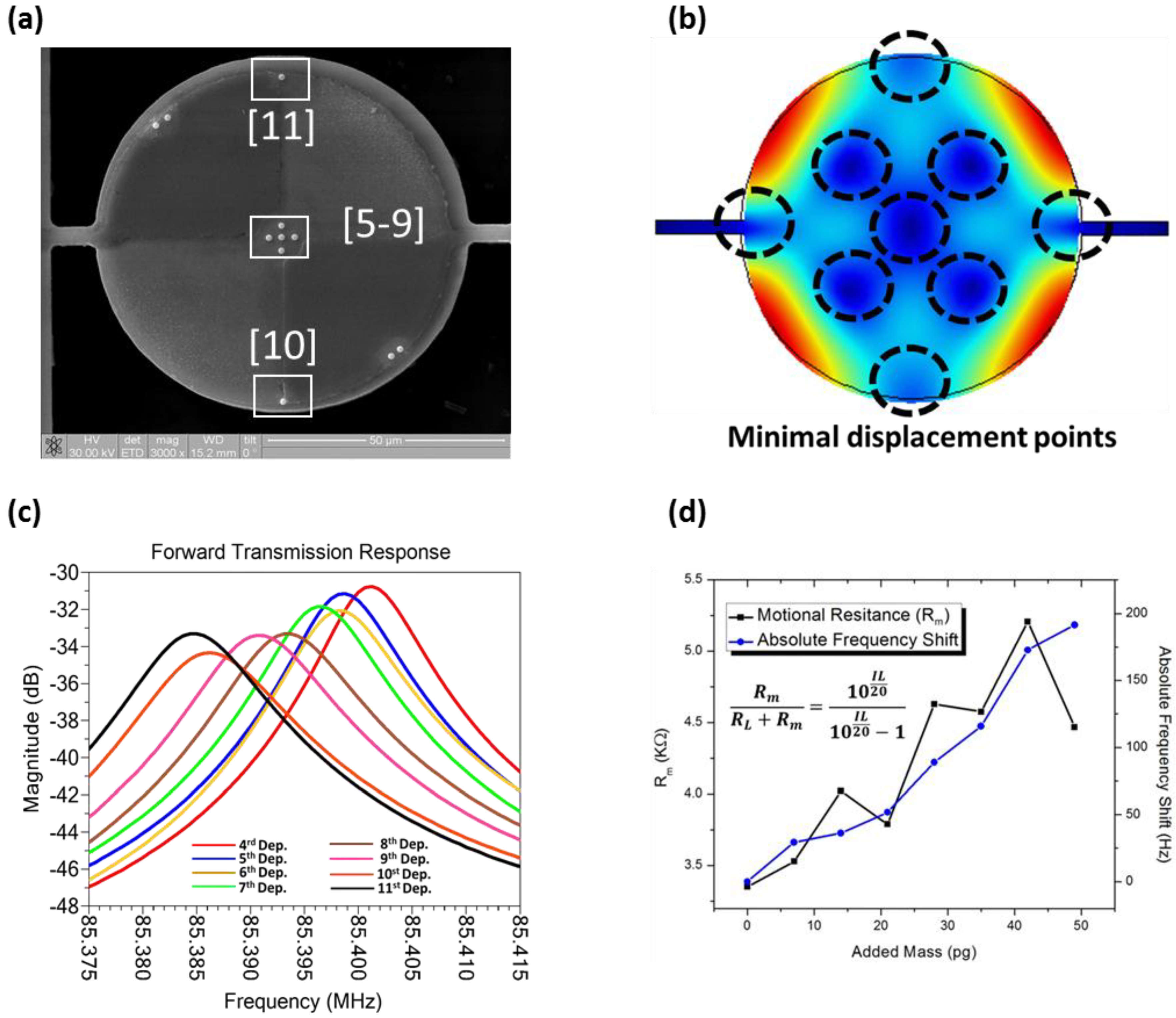
Figure 8.
(a) SEM image of showing the location of sequentially deposited Pt/Ga micro-pellets at the maximum displacement points; (b) COMSOL® modal simulation illustrating the maximum displacement areas of the corresponding fourth-order contour mode; (c) measured frequency responses showing the frequency drift induced by the added extra mass of each micro-pellet; (d) measured absolute frequency shift and motional resistance (Rm) of the device versus loaded mass verifying negligible impacts of the micro-pellets made to the signal strength (insertion loss) and energy dissipation (Q-factor).
As shown in
Figure 8c,d, the extra loaded masses introduced by the micro-pellets in this fashion made negligible impacts on the Q factor and the effective motional impedance while resulting in consistent resonant frequency drop for each micro-pellet deposited. On the opposite side, it can be observed that when the loaded mass by the micro-pellets were added at locations adjacent to the nodal points of the disk resonator in its fourth contour mode as shown in
Figure 9a, the mass loading significantly affects the energy dissipation and therefore the Q factor and motional impedance the device while producing much less severe resonance frequency shift and poor mass sensitivity of 0.334 Hz·fg
−1, thus negatively impacting the achievable resolution of the contour-mode resonator based mass sensor.
Figure 9.
(a) SEM image of showing the location of sequentially deposited Pt/Ga micro-pellets adjacent to the minimum displacement points; (b) COMSOL® modal simulation illustrating the minimum displacement areas of the corresponding fourth-order contour mode; (c) measured frequency responses showing the frequency drift induced by the added extra mass of each micro-pellet; (d) measured absolute frequency shift and motional resistance (Rm) of the device versus loaded mass showing the impacts of the micro-pellets on the insertion loss and energy dissipation (Q-factor).
Aside from the sensitivity, another important performance metric for a resonant mass sensor is the linearity of its output signal in response to the infinitesimal amount of loaded mass. By introducing FIB deposited identically-sized micro-pellets at strategically-chosen maximum displacement locations, highly repeatable frequency shifts linearly proportional to the loaded mass have been achieved while retaining the other key performance parameters, such as Q factor and motional impedance. Meanwhile, the binding site at which the external analyte is attached to the resonator body is proven to play a crucial role in affecting the effective sensitivity, linearity and repeatability in the resonant response of the lateral extensional mode sensor.
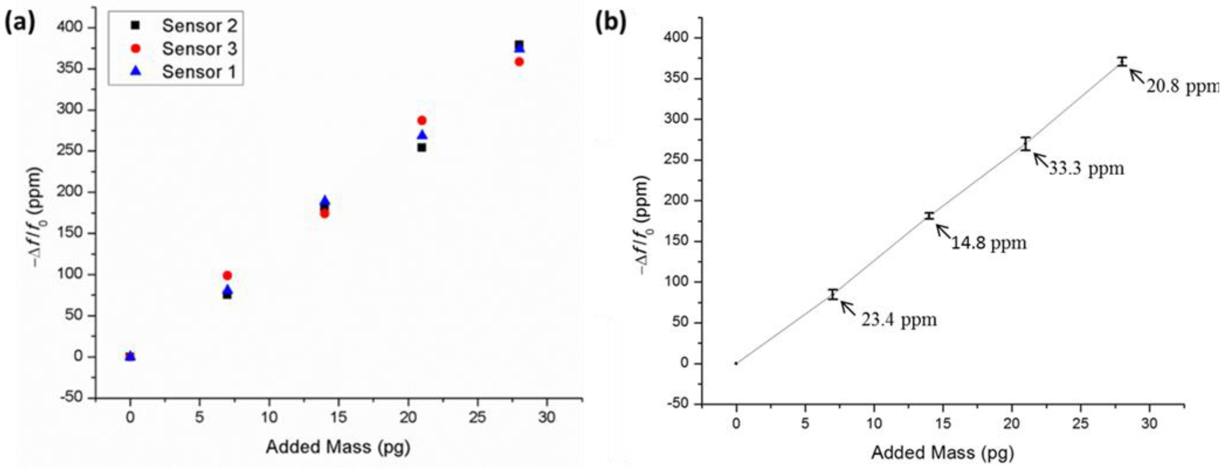
Figure 10.
(a) Measured fractional frequency shifts versus added mass; and (b) y-error of the mass-loading induced fractional frequency shift for three 40 μm-radius disk resonator based mass sensors operating at the fourth-order contour mode.
Figure 10.
(a) Measured fractional frequency shifts versus added mass; and (b) y-error of the mass-loading induced fractional frequency shift for three 40 μm-radius disk resonator based mass sensors operating at the fourth-order contour mode.
For instance, when the micro-pellets were deposited adjacent to central and circumferential nodal points as seen in
Figure 9a, we observed a much more nonlinear mass-loading induced frequency shift along with noticeable Q-factor degradation and motional impedance variation. We attribute this to the increased energy dissipation due to the higher energy losses for an unbalanced and distorted resonating microstructure. To the best of our knowledge, this is the first time such an effect has been observed because previous works have only focused on exploring a single region of the maximum displacement area [
11,
12,
19]. As seen in
Figure 9c,d, the total loaded mass of 35 pg from 5 FIB micro-pellets near the central nodal points (
i.e., location 5-9) has essentially reduced the loaded Q factor from 10,000 to merely 6000 along with an abrupt increase of the motional impedance from 3.5 kΩ to 4.5 kΩ.
The subsequent FIB depositions of two more micro-pellets at location 10 and 11 near the circumferential nodal points as seen in
Figure 9a have led to slightly higher frequency shifts but also inconsistent behavior. We observed that the micro-pellet deposited at location 10 disrupts the resonant mode to cause damping, Q-factor degradation and an increased motional impedance of 5.1 kΩ. We also observed that the second micro-pellet at location 11 recovered the balance of the modal vibration thus bringing the Q-factor and motional impedance back to their nominal values of 6000 and 4.5 kΩ prior to these FIB micro-pellet depositions. In some of the prior works, the entire surface of the resonator body was employed as the binding site in an indiscriminate fashion for weighing target analytes, which could lead to severe uncertainty and degraded sensitivity as evidenced by the measurement results shown in
Figure 8 and
Figure 9 [
20,
21]. Based on our new findings, it is clear that the strategic design of the binding location of target analytes should be deemed a crucial step for adapting contour mode MEMS resonators for practical mass sensing applications. To evaluate the repeatability of these mass sensor devices, two more devices were tested as presented in
Figure 10, where four micro-pellets were deposited at the maximum displacement areas of the fourth-order contour mode.
Figure 10 presents the fractional frequency changes for all three sensors as a function of the loaded mass from FIB deposited micro-pellets at their corresponding maximum displacement points. As seen in
Figure 10a, the sensors demonstrated consistent and close-to-linear mass-loading induced frequency shifts with very small variations based upon the counter balance effect due to the inaccurate placements of the micro-pellet deposition. As shown in
Figure 10b, a device-to-device discrepancy less than 33.3 ppm was observed, which can be largely attributed to the fabrication tolerance (device-to-device geometry variation) and the placement precision of each added micro-pellets with respect to modal locations of the desired resonance mode. In addition, the composition of the micro-pellets could change slightly as a consequence of variation of the FIB chamber conditions.
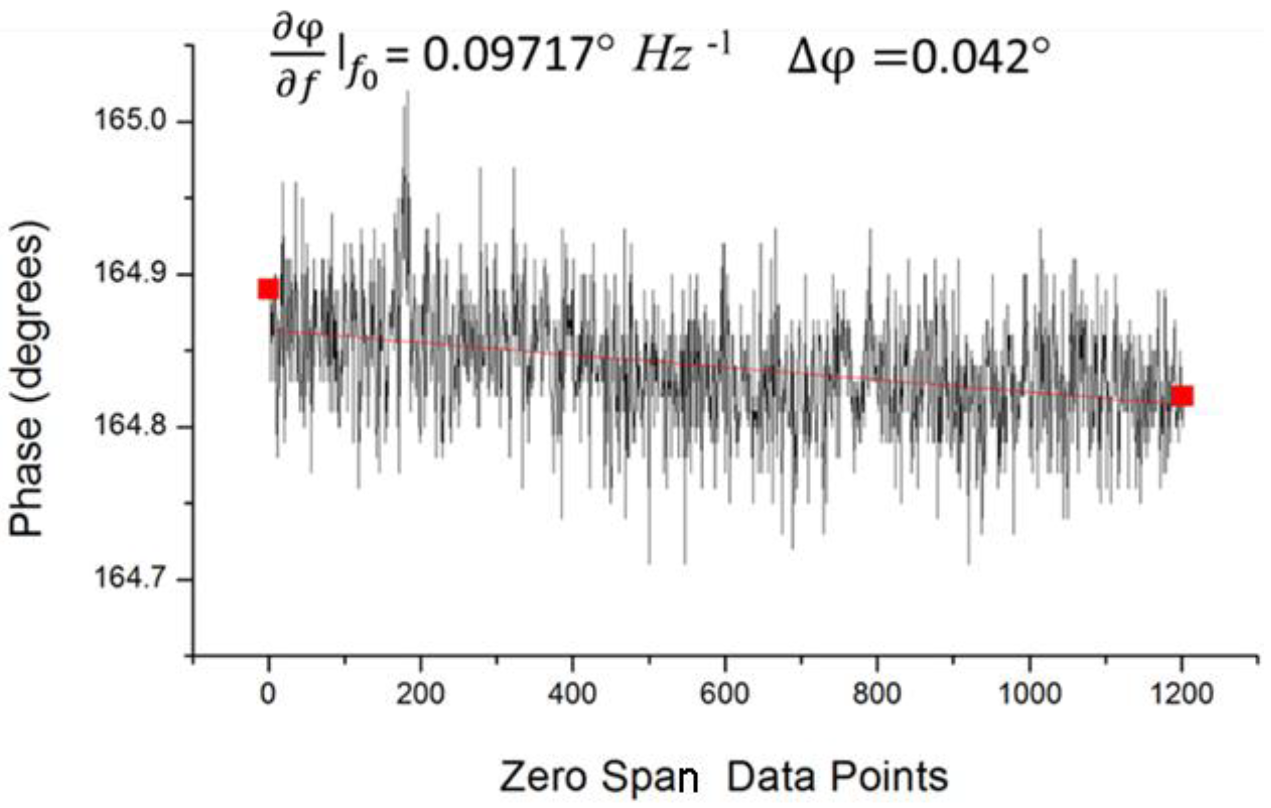
The mass resolution of the resonant sensor can be obtained by determining the short-term resolution through the slope of the phase at the resonance given by [
19]:
where
is the slope of the phase at the resonance frequency and
is the zero span phase noise.
Figure 11.
Measured phase noise and slope at 85.4 MHz.
Figure 11.
Measured phase noise and slope at 85.4 MHz.
The measured zero span phase noise at the nominal resonance was 0.042° and the slope at resonance was calculated to be 0.09717°·Hz
−1 as shown in
Figure 11. Therefore, the short term frequency noise for the sensor was estimated to be 0.43 Hz. Based on this value, the point mass sensitivity of this device can be estimated to be 367 ag and 1290 ag at the maximum and minimum displacement areas, respectively. It is important to note here that the Q factor plays a crucial role on the stability of the sensor signal. As the resonator Q degrades as a result mass loading on the nodal points, so will the slope of the phase at resonance, which results in reduced mass resolution.


