Article

Surface Characterization and Secondary Electron Emission Properties of Alumina Containing MgO Film on Ag-Mg-Al Alloy

Key Laboratory of Advanced Functional Materials of Education Ministry of China, Beijing University of Technology, Beijing 100124, China
*
Author to whom correspondence should be addressed.
Metals 2018, 8(8), 570; https://doi.org/10.3390/met8080570
Submission received: 28 June 2018 / Revised: 17 July 2018 / Accepted: 19 July 2018 / Published: 25 July 2018
(This article belongs to the Special Issue 5th UK-China Steel Research Forum)

Abstract

:
Ag-Mg alloy is used as a dynode material in electron multiplier tubes due to the high secondary electron yields (δ) of the surface of MgO film. However, MgO film is readily degraded under strong electron or ion bombardment, which results in a decrease in the lifetime of devices. In this study, alumina-containing MgO films of ~50–150 nm were developed on a Ag-2Mg-2Al alloy (silver alloy containing 2 wt % Mg and 2 wt % Al) after a thermal activation process performed at 500–600 °C under low oxygen pressures of 5.0–20.0 Pa. Auger electron spectroscopy and X-ray photoelectron spectroscopy analyses reveal that the film consists of a thin layer of pure MgO and a relatively thicker layer of alumina-containing MgO located beneath the top MgO layer. The alumina-containing MgO film exhibits high δ value of 7.7 at a primary electron energy of 580 eV and a much better stability under energetic electron bombardment than pure MgO film on Ag-Mg alloy. Alumina has higher bond dissociation energy than MgO, and the presence of alumina in the film contributes to mitigating the dissociation of the MgO film under electron bombardment. The Ag-2Mg-2Al alloy with alumina-containing MgO film is a promising candidate as a dynode material for electron multiplier tubes.

Graphical Abstract

1. Introduction

The secondary electron emission (SEE) process is important for various vacuum electronic devices, such as scanning electron microscopes, atomic clocks, alternating current plasma display panels, and electron/photomultipliers for mass spectroscopy, photoelectron spectrometers, magnetrons, and crossed-field amplifiers [1,2,3,4,5]. A variety of materials are selected to satisfy specific requirements for enhancing or suppressing the secondary electron yield (δ) [6]. Low δ materials are desirable for a dielectric window in high-power microwave devices in order to suppress surface breakdown at the vacuum/dielectric interface [7]. On the other hand, materials with high δ and good stability under exposure to energetic electron beam and charged particles, such as BeO [8], MgO [9,10], Al2O3 [11], and chemical vapor deposition (CVD) diamond films [12], are required for various electron multipliers. Materials of high δ and good stability are the focus of our interest in this study.
Ag-Mg alloys, normally with 2–4 weight percent of Mg, have been utilized as one of the alloy-type secondary electron emitters since the 1950s. An activation process involving the selection of an oxidizing atmosphere and temperature must be done properly in order to favor the growth of MgO film, normally 20–200 nm thick, at the surface, rather than in the bulk of the alloy [9,13]. The developed MgO thin films exhibit high δ values of 15–20 [14]. The activation process involves two major processes—the migration of Mg to the surface and the counterflow of oxygen into the Ag substrate. Major factors influencing the formation of the MgO film include the oxidizing atmosphere, the atmosphere pressure, and the oxidizing temperature [9,15]. Nowadays, various deposition methods have been used for preparing MgO thin films, such as electron-beam evaporation [16,17], sol-gel deposition [18], and magnetron sputtering [19,20,21]. However, MgO films prepared through activation on Ag-Mg alloys and by various deposition methods are readily dissociated under constant bombardment from electron beam and ionized particles, which restricts their practical applications in vacuum electron devices. MgO/Au cermet film, which consists of a mixture of MgO and Au microcrystals, has been reported to have high δ values with good electric conductivity [22,23]. However, considerable erosion and dissociation of MgO in the film is found under constant electron beam bombardment [24], and considerable degradation of δ occurs in a short period [25]. Pan studied the SEE properties of the Cu-Al-Mg alloy and found that MgO/Al2O3 composite film is developed spontaneously at room temperature without activation, and the alloy emitter has excellent stability with δ values over 3 under constant electron bombardment [26]. Higher amounts of Al and O in the surface of the Cu-Al-Mg alloy are reported to be associated with its excellent working stability.
A systematic study of the SEE properties of MgO/Al2O3 composite films has so far not been reported, and experiments are being conducted in this direction. Similar to MgO, alumina is an insulator with good physical and chemical properties, such as low electrical conductivity, high thermal conductivity, high SEE yields, wide bandgap, and thermodynamic and chemical stability [11,27]. In this study, Ag-Mg-Al alloy was prepared and properly activated in low oxygen pressure (PO2). The δ of the Ag-Mg-Al alloy cathode as a function of the primary electron energy (Ep) was examined. The stability of the Ag-Mg-Al emitter under electron bombardment was tested and compared to that for a Ag-Mg emitter. Superior SEE properties, including high δ and better stability under electron bombardment, were found for the Ag-Mg-Al emitter with proper film thickness. Here, the film composition and element distribution in the film are characterized and the effect of Al in the film on the SEE properties of the alloy is discussed.

2. Materials and Methods

2.1. Specimen Preparation

Alloy blocks of Ag-Mg-Al alloy containing approximately 2 wt % Mg and 2 wt % Al (denoted as Ag-2Mg-2Al) and Ag-Mg alloy containing approximately 3 wt % Mg (denoted as Ag-3Mg) were prepared by induction melting of a Ag sheet (99.99% in purity, Jiaming Boye Non-ferrous Metals Ltd., Beijing, China), Mg pellets (99.98% in purity, Sigma-Aldrich Inc., Shanghai, China), and Al powder (99.95% in purity, Sigma-Aldrich Inc., Shanghai, China), in designed weight percentage, at 1050 °C for 1 min in a low-pressure argon atmosphere (99.999% in purity, Huiya Industrial Gas Co., Zhuo Zhou, China) using an induction melting furnace (SP-15VIM, HF-Kejing, Hefei, China). Due to evaporation loss during the melting process, 5 wt % more Mg was taken into account. Surface scales of the alloy blocks were removed by polishing before they were cold rolled to sheets of ~0.4 mm thick. The alloy sheets were baked at 500 °C for 2 h in an argon atmosphere in order to eliminate the work hardening of the alloy sheets. The alloy sheets were cut into pieces with dimensions of 1.0 cm × 1.0 cm, followed by polishing with sandpaper of 2000#, 3000#, respectively. The alloy pieces were ultrasonic cleaned in ethanol for 2 min, and then dried in cool air and kept in a vacuum desiccator.
Activation of the alloy pieces was performed in a corundum tube furnace, initially evacuated by a mechanical pump to a base pressure of 0.1 Pa. The specimens were baked at 500–650 °C for 0.5 h at PO2 of 5.0–25.0 Pa by filling the chamber with oxygen flow controlled through a dedicated flow meter. The specimens were cooled down before they were taken out, and then kept in a vacuum desiccator immediately.

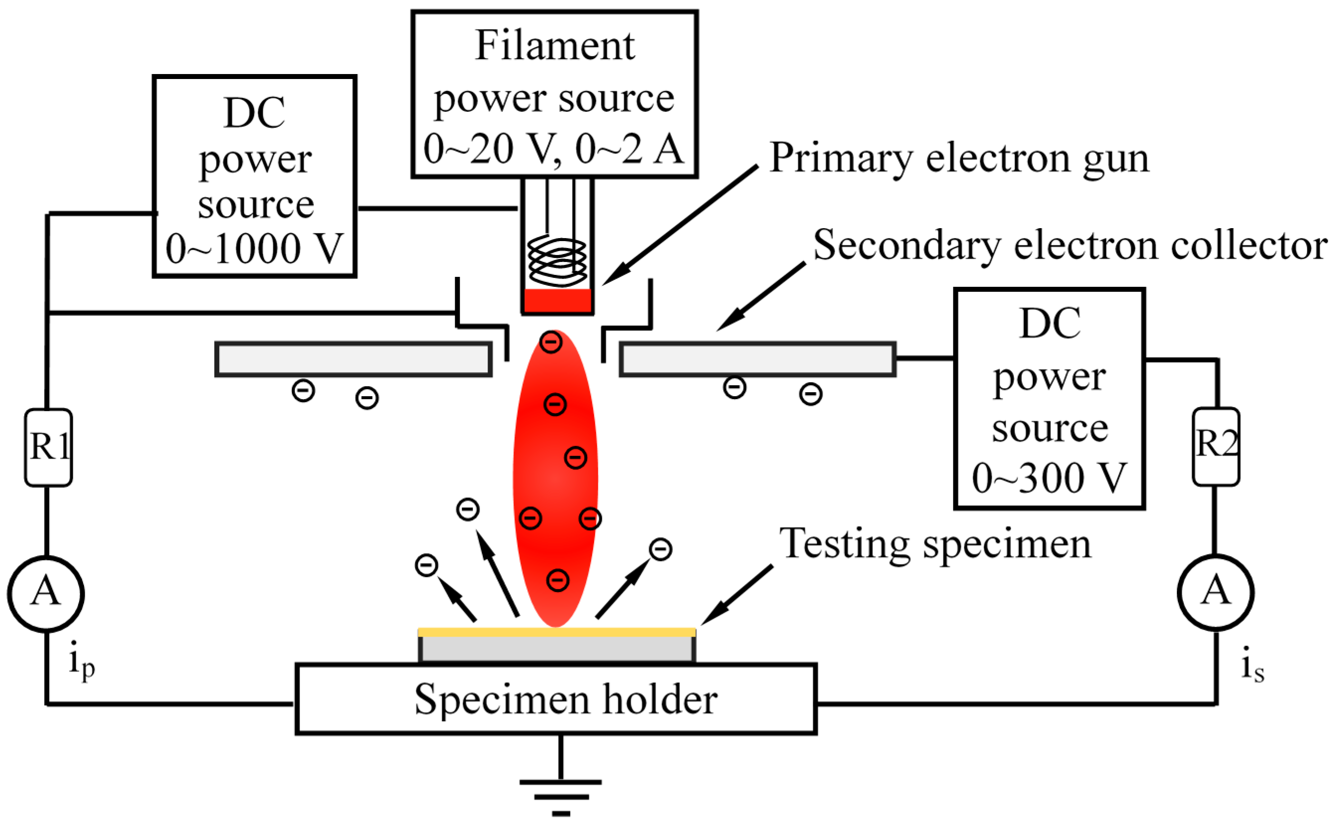
2.2. SEE Testing Arrangement

The SEE properties of the specimens were measured by a self-designed SEE testing system, shown in Figure 1. The primary electron beam is provided by a Ba-W dispenser cathode working at ~500 °C. The whole system was mounted in a chamber with a vacuum pressure of less than 1.0 × 10⁻⁵ Pa, obtained by pumping with a turbo molecular pump backed by a rotary mechanical pump. The emission testing was carried out with accelerating voltages in the range of 0–1000 V, and the secondary electron current from the tested specimens was collected by a secondary electron collector applied at a voltage of 250 V. The δ was obtained by measuring the primary electron current (ip) and the emitted secondary electron current (is), and the δ is the ratio of is to ip. The stability of the specimens under electron bombardment was examined by constant bombardment of the specimens by a primary electron beam of 600 eV and a current density of 5 mA cm−2. The δ of the specimens was recorded every several hours during the electron bombardment testing.

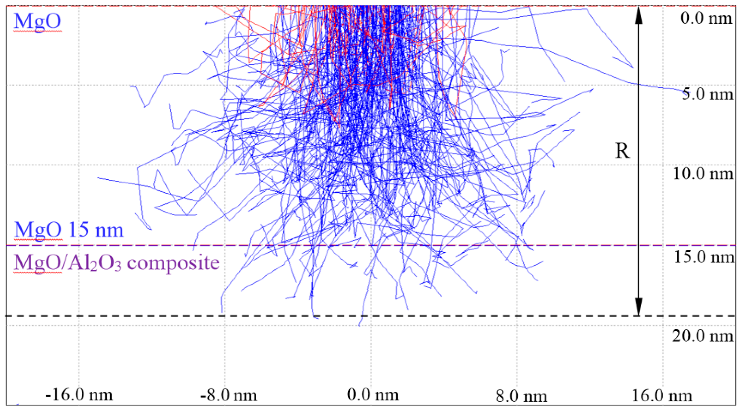
2.3. Surface Characterization and Secondary Electron Distribution Simulation

The surface morphology of the activated Ag-Mg-Al specimens was examined by scanning electron microscopy (SEM) using a Hitachi S-4800 instrument (Tokyo, Japan). The surface composition of the specimens was examined by Auger electron spectroscopy (AES) using an ULVAC-PHI-700 instrument (Chigasaki, Japan). The chemical state of the major elements in the surface film was analyzed by X-ray photoelectron spectroscopy (XPS) using an ULVAC-PHI Quanera instrument (Chigasaki, Japan). The specimens were evacuated to 5.0 × 10⁻⁷ Pa, and the depth profiles of the specimens derived from AES and XPS were obtained by assisted sputtering by argon ions at a sputtering rate of 5 nm min−1.
Secondary electron distribution in the surface film of the Ag-2Mg-2Al specimen subject to electron beam bombardment of 600 eV was simulated by computational simulation using a CASINO Monte Carlo program v2.42 (Cambridge, UK) [28]. The film composition and film thickness were designed according to the result from AES depth profiles.

3. Results and Discussion

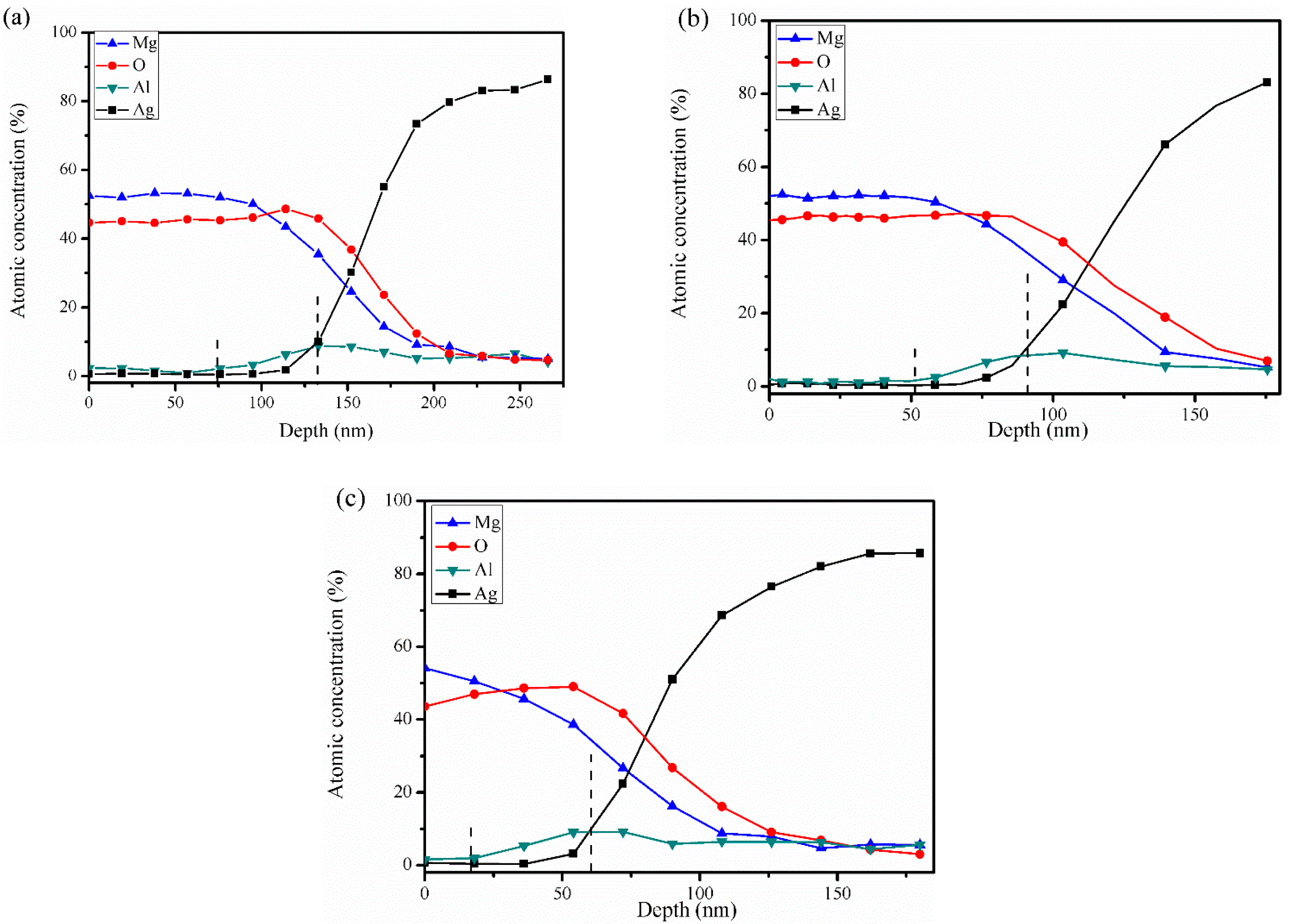
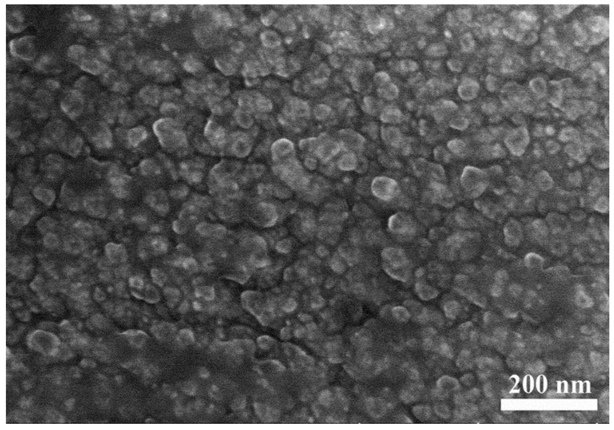
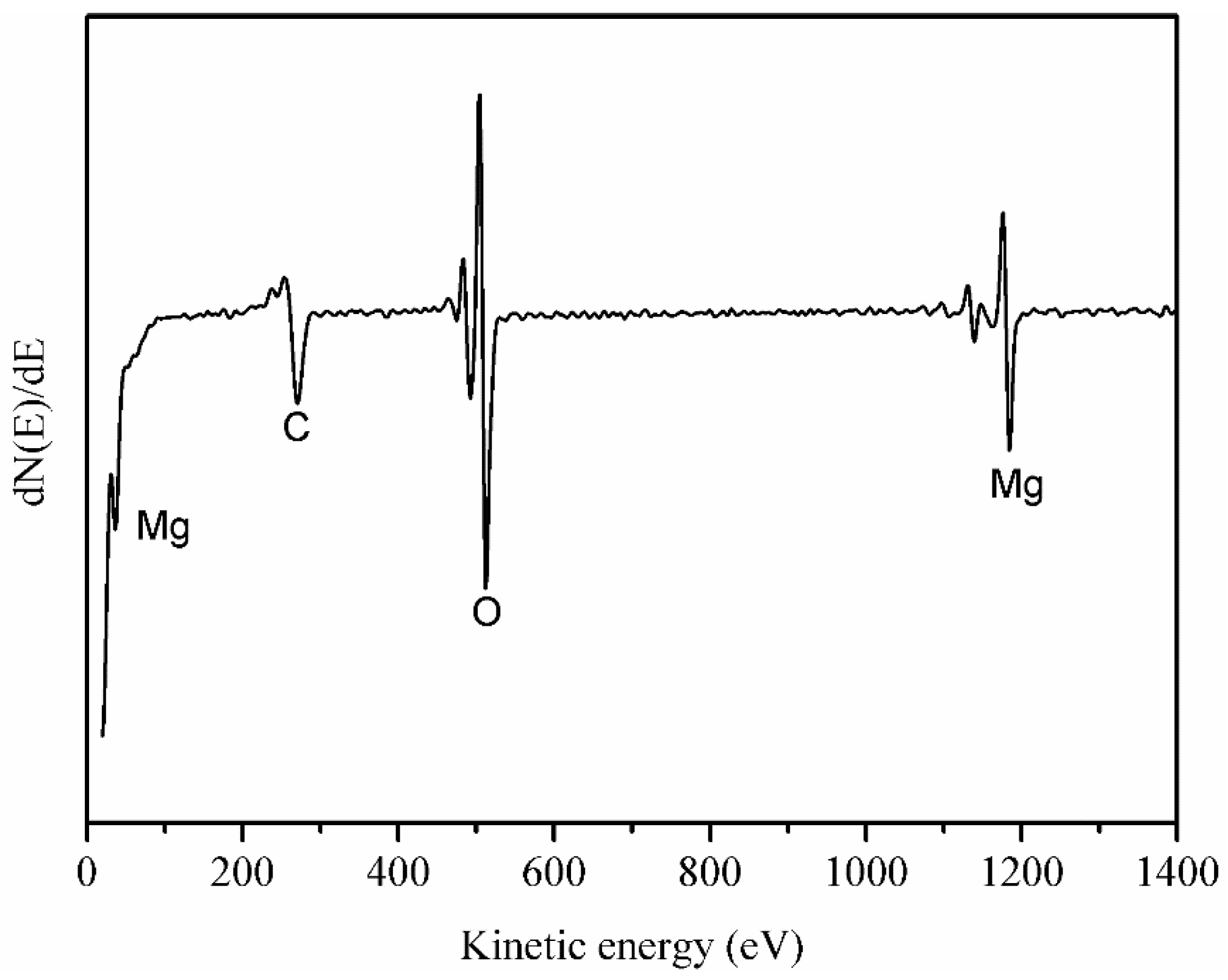
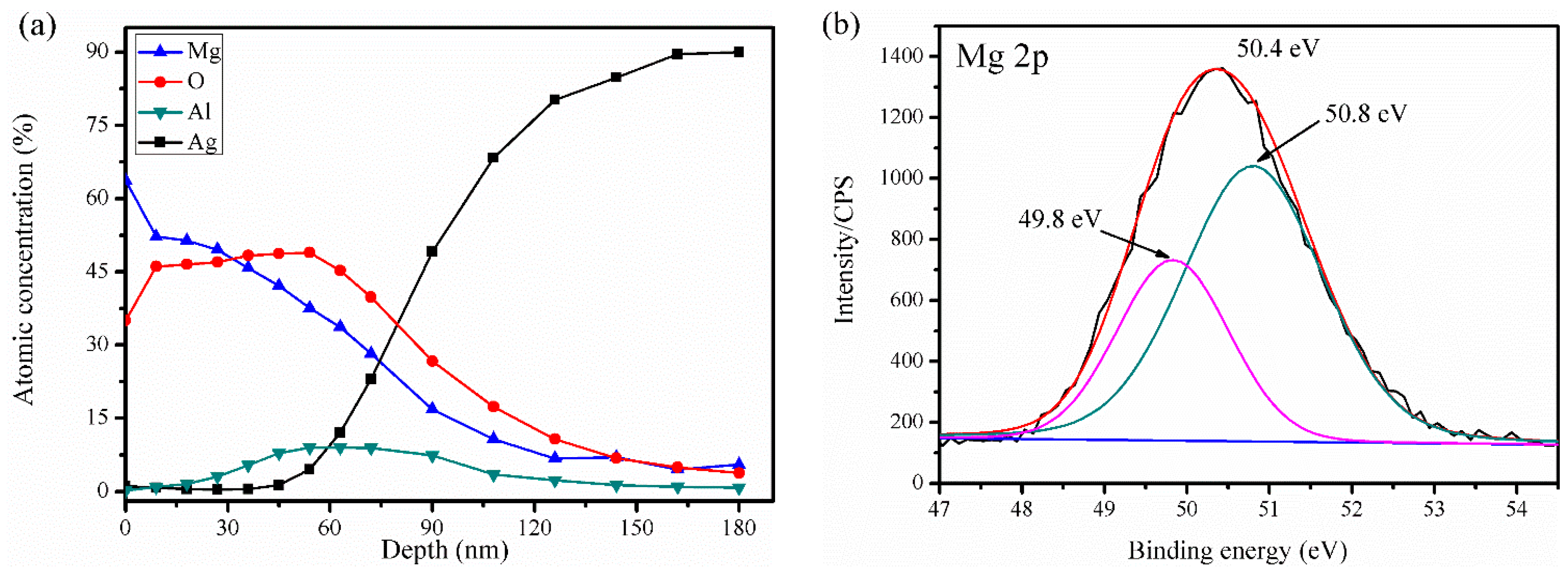
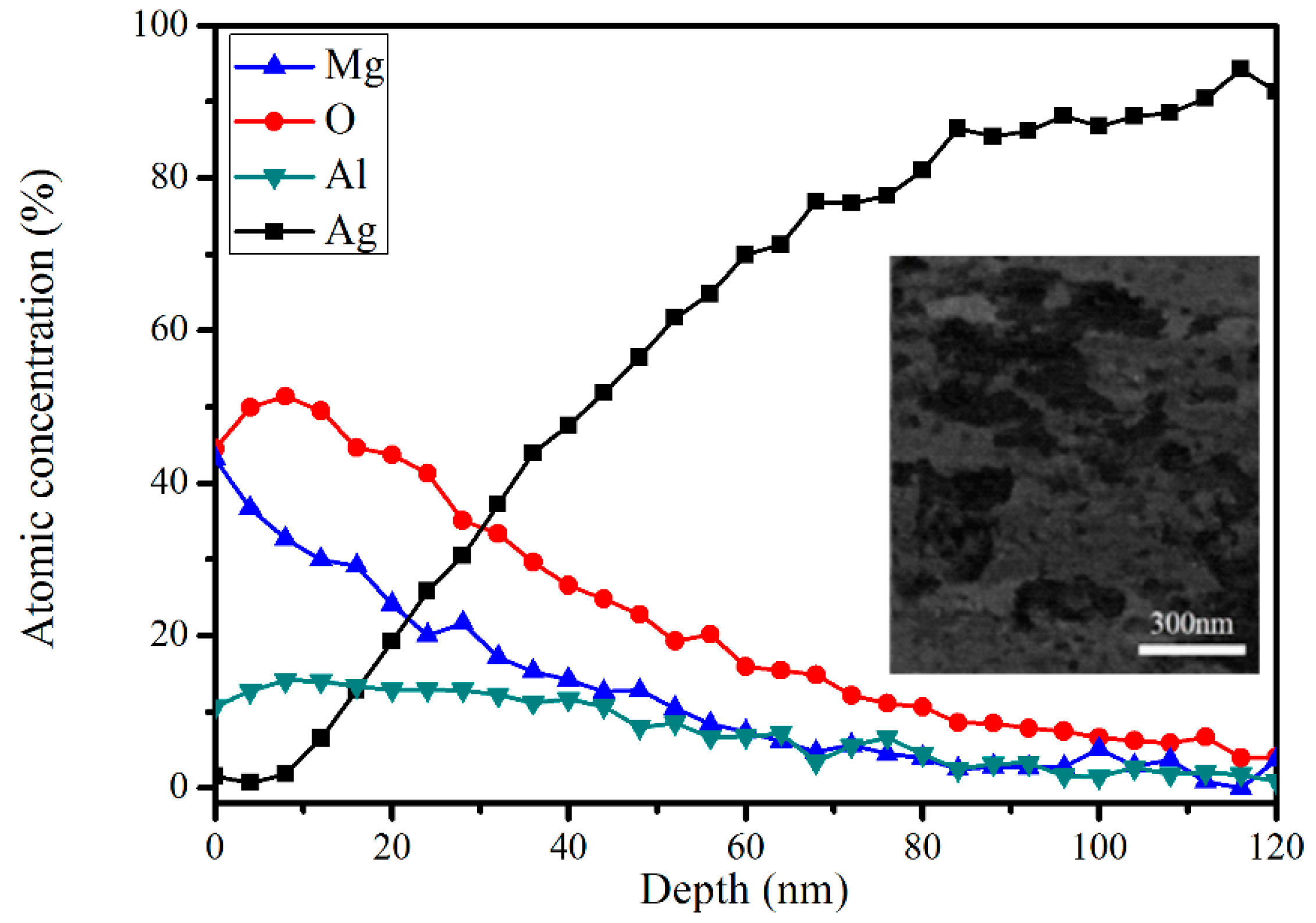
3.1. Surface Morphology and Composition

The surface color of the Ag-2Mg-2Al alloy specimen turned from silvery white to translucent flaxen after activation. The scanning electron micrograph in Figure 2 shows a typical surface morphology of Ag-2Mg-2Al alloy specimens activated at 500–600 °C for 0.5–1.0 h at PO2 = 5.0–25.0 Pa. Unique round-shaped flakes of ~20–60 nm were developed on the surface after activation, which is similar to the surface morphology of activated Ag-3Mg alloy [15]. A typical AES spectrum of the surface of the activated Ag-2Mg-2Al specimen in Figure 3 reveals that the surface is mainly composed of Mg and O. The C peak is due to the inevitable absorption of carbon species onto the surface when the specimen is taken out of the furnace tube after activation. No Ag or Al is detected in the AES spectrum. These results infer that pure MgO was developed in the top surface after activation. Mg has a rather high vapor pressure as compared to most other metal elements. The vapor pressure of Mg at 600 °C is 114 Pa, according to the vapor pressure equation for Mg [29], which is much higher than that for Al. Mg becomes mobile at elevated temperature and low pressure, and it migrates towards the surface at much more rapid rate than Al during activation. Therefore, a thin layer of pure MgO is developed in the top surface of the Ag-2Mg-2Al alloy after activation.
The flake morphology of the surface can be explained by the Pilling–Bedworth ratio (PBR) of oxide film. Metal oxides with a PBR in the range of 1–2 can develop compact barrier film on its metal, such as amorphous alumina film on aluminium, which has a PBR of 1.61. As the PBR of MgO film is 0.81 [30], it cannot cover the whole metal surface, and the flake characteristic is developed for the film on the activated Ag-2Mg-2Al alloy.

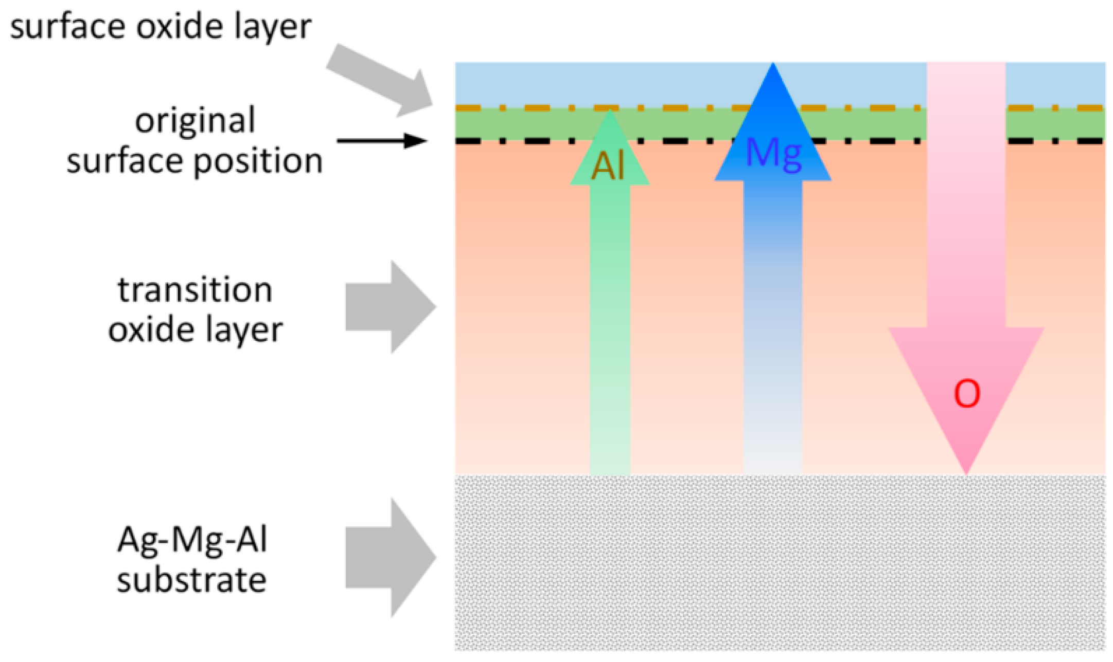
3.2. Oxidation Process during Thermal Activation

Figure 4 shows element depth profiles of the activated Ag-2Mg-2Al specimens derived from AES. The depth profiles reveal a general trend that the top surfaces of the alloys, being several tens of nanometers thick, are composed entirely of Mg and O, while Ag and Al are negligible in these regions. The atomic ratios of Mg to O in the top surfaces are ~0.8–1.2, which indicates the formation of MgO in the surface. During activation, Mg atoms in the substrate become mobile and migrate towards the surface, while O molecules migrate inwards from the surface simultaneously [13]. MgO is developed in the top surface as a result. The amount of Mg being slightly higher than that of O in the top layers is probably due to the outward migration of Mg atoms being rapid at elevated temperatures, and a small portion of Mg is not oxidized, as the oxygen is not sufficient at relatively low oxygen pressures of 5.0–25.0 Pa [31]. Al and Ag signals do not appear until a certain depth, which is consistent with the result from the surface AES spectrum in Figure 3. Moreover, Al always rises at depths closer to the surface than Ag. The depths from where Al originates are marked as short dashed lines in the profiles in Figure 4. Ag is considered immobile during activation due to its inert characteristic and heavy atomic weight. Therefore, it is inferred that both Mg and Al atoms migrate outwards during activation, and Mg migrates at a much higher rate than Al, which is similar to the findings for the anodizing of Al-Mg alloys [30]. The film formation process during activation of the Ag-2Mg-2Al alloy is schematically illustrated in Figure 5.
The thickness of the MgO film on the alloy is defined as the thickness of the layer from the surface to the interior position at which Ag content reaches 10 atom %. The MgO film has a much lower electrical conductivity compared to Ag in the alloy matrix. Electron supply to the electron-deficient surface is hampered, and the surface charging effect is serious if the surface MgO layer is too thick or the Ag content is below 10 atom % in the MgO film [22]. Based on the definition, the bottom position of the MgO film was determined, and it is marked by long dashed lines in the AES depth profiles in Figure 4. Normally, thicker MgO film is obtained when Ag-Mg alloy is activated at higher temperatures and larger PO2 for a longer time. A MgO film of 60 ± 1 nm was obtained for the Ag-2Mg-2Al activated at a relatively low temperature of 500 °C for 30 min at PO2 = 20.0 Pa. The thickness of the MgO film is increased from 60 ± 1 nm to 90 ± 1 nm as the activation temperature is increased from 500 to 600 °C. Notably, Al originates at a depth of ~15 nm for the alloy activated at 500 °C, which is closer to the surface compared to that for the alloy activated at 600 °C. As the PO2 is increased from 15.0 to 20.0 Pa, the thickness of the MgO film is reduced from 133 ± 1 nm to 90 ± 1 nm and Al originates at a depth of ~51 nm, which is relatively close to the surface. This is probably because the rate of oxygen migrating into the substrate is increased under higher PO2, and more Mg and Al atoms are oxidized. More Mg and Al oxidized in the film slows down the outward migration of Mg, resulting in a relatively thinner oxide film for the alloy activated at higher PO2. The thickness of the MgO film and the depth at which Al originates in the surface film of the Ag-2Mg-2Al specimens activated at different parameters are summarized in Table 1. It indicates that due to the presence of Al in the Ag-2Mg-2Al alloy, thicker MgO film could be obtained by increasing the temperature or reducing the PO2 during activation. When the PO2 is increased or the temperature is decreased during activation, Al originates closer to the film surface.
The chemical state of Mg and Al in the surface films of the activated Ag-2Mg-2Al alloys was analyzed by XPS. Figure 6a,b reveals XPS spectra of Mg 2p and Al 2p in the surface film, respectively, for the Ag-2Mg-2Al specimen activated at 500 °C for 30 min at PO2 = 20.0 Pa. The XPS spectrum of Mg 2p was obtained from the specimen sputtered to a depth of 10 nm, and it reveals that the Mg 2p peak is located at 50.7 eV, which corresponds to the binding energy of MgO [26,32,33]. The XPS spectrum of Mg 2p agrees well with the result from the AES depth profiles in Figure 4. XPS was performed at a depth of 40 nm for Al 2p, and it revealed the Al 2p peak is located at 74.8 eV (Figure 6b), which is in agreement with the binding energy of Al in Al2O3 [26,34]. It confirms that Al has been oxidized to Al2O3 in the film after activation. The chemical state of Ag was determined by the Ag MNN Auger spectrum for the specimen at a depth of 70 nm (Figure 6c). The Ag peak at 351.9 eV in the Ag MNN Auger spectrum confirms that Ag is in its elemental state [35]. This indicates that Ag in the substrate was not oxidized during activation, which is due to its rather low chemical affinity for oxygen. The results from the XPS spectra and AES depth profiles in Figure 4 confirm that an oxide film is developed on the Ag-2Mg-2Al alloy after the activation process, with a pure MgO layer in the top surface and a relatively thicker layer of MgO/Al2O3 composite located beneath the top MgO layer (Figure 5).

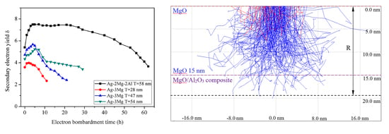
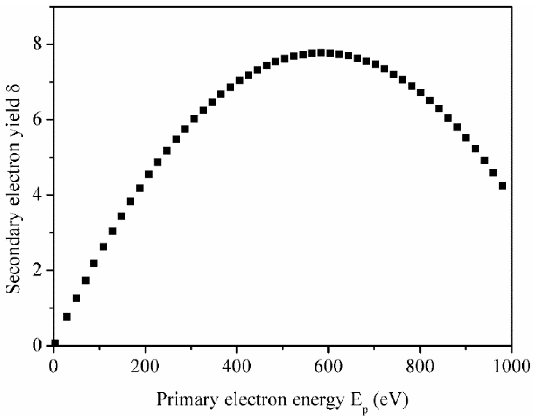
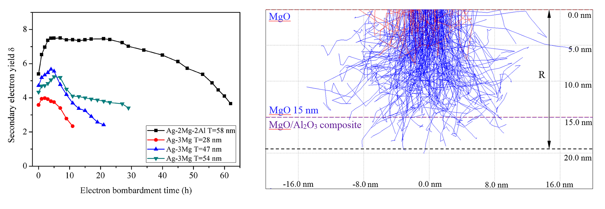
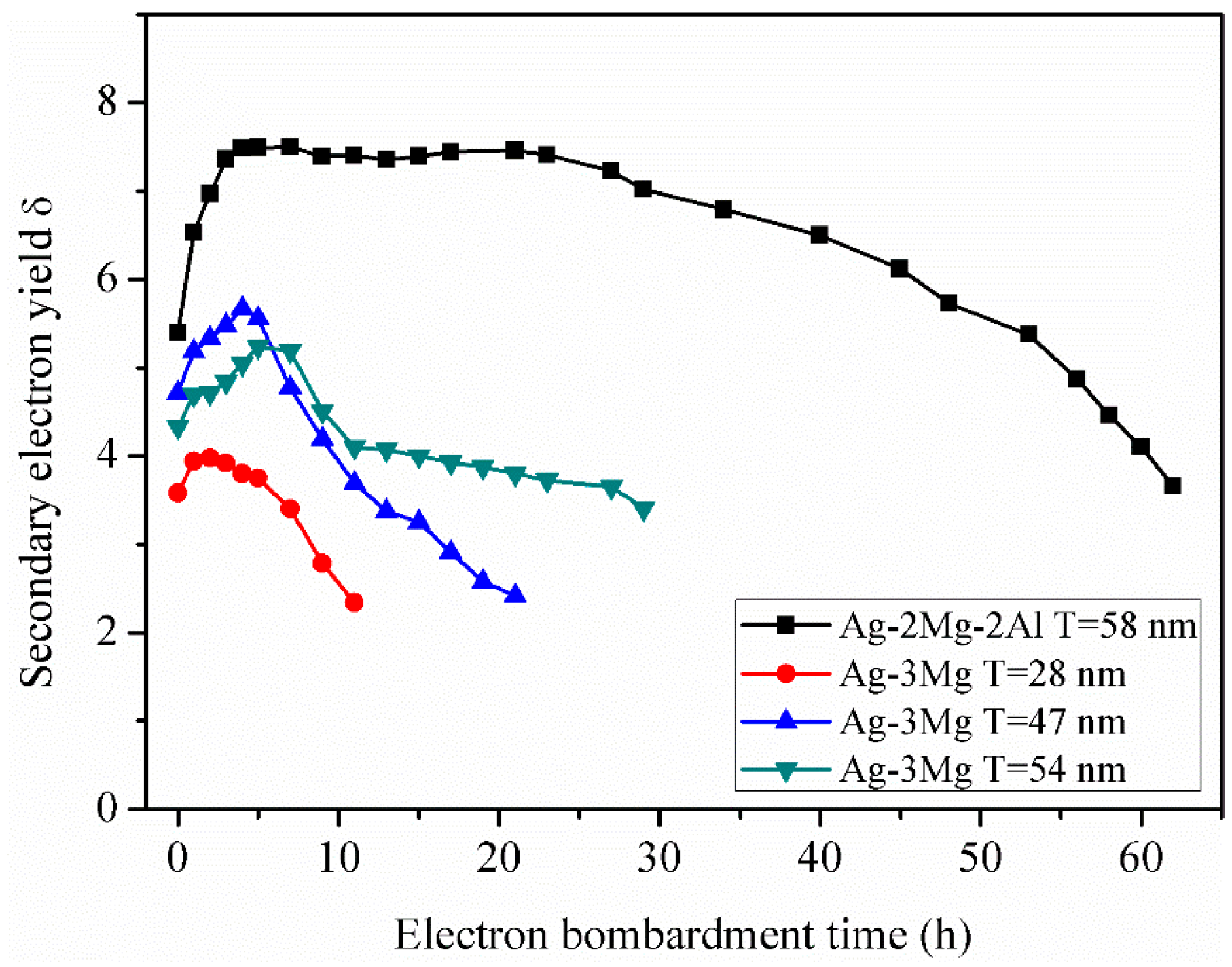
3.3. Secondary Electron Yield and Electron Bombardment Performance

Values of δ varying from 4.0 to 10.0 were obtained for the Ag-2Mg-2Al and Ag-3Mg alloys activated at 500–600 °C and at PO2 between 10.0–20.0 Pa. An ‘aging’ process was carried out before SEE testing, in which the specimens were bombarded by primary electrons of 200 eV for several hours. δ gradually increases before it becomes steady after several hours. It is probably due to surface contamination, such as carbon species and residual metallic Mg on the surface, which are eliminated after aging.
Typical δ as a function of the Ep for the Ag-2Mg-2Al alloy cathode after aging is shown in Figure 7. The total yield includes elastically and inelastically scattered electrons, as well as low energy true secondary electrons [36]. Initially, δ increases with increasing Ep, when the primary electron penetration range is less than the mean escape depth for the excited secondary electrons [5]. A δm value of 7.7 is reached at Ep = 580 eV, when the primary electron penetration range is close to the escape depth. δ decreases with further increasing Ep, as secondary electrons excited at the escape depth become fewer [6,7]. The escape depth for secondary electrons depends on the type of material of the emitter. Except the Ep and the bias voltage, other factors influencing the δ of the emitter include the film thickness [16], the electronic structure of the film [37], the incident angle of primary electron beam, surface roughness, and crystallinity of the surface oxide [10]. Figure 7 reveals that the Ag-2Mg-2Al specimen has a δ value of 6.0 at Ep = 300 eV, which proves its suitability as an efficient secondary emitter at sufficiently low input electron energies.
The emission stability of the Ag-3Mg and Ag-2Mg-2Al specimens with different film thicknesses was examined by constant bombardment of the specimens by a primary electron beam of 600 eV and a current density of 5 mA cm−2. The δ variation curves over time are shown in Figure 8. For the tested specimens, δ initially increases and optimal δ is reached after ‘aging’ by irradiation with a primary electron beam for several hours. The specimen with thicker MgO film requires a relatively longer time of aging to reach its optimal δ value. For the Ag-Mg specimens, δ begins to decrease promptly after a maximum value is reached. The δ value drops less steeply for the Ag-3Mg specimen with relatively thicker MgO film. Comparatively, there is a plateau region for the activated Ag-2Mg-2Al specimen after the aging period, with δ remaining at a high level for over 20 h. The δ of the Ag-2Mg-2Al specimen with a 60 nm thick MgO layer remains for over 4 h after bombardment by energetic electron beam for 60 h, which is much longer than that for the Ag-3Mg specimens. Figure 8 clearly reveals that the Ag-2Mg-2Al specimen has superior SEE properties, including not only higher δ values of over 7, but also good emission stability, with δ maintaining high values between 7.0 and 7.8 for ~30 h.
The penetration depth of primary electrons as a function of Ep can be approximately expressed by the following equation [38]:
R = 115 × ( E P ) 1.35 / ρ
where R is the penetration depth in nm, Ep is the energy of primary electrons in keV, and ρ is the density of the solid bombarded by primary electrons. According to the classical equation, the penetration depth is 16.0 nm at Ep = 600 eV for MgO film (the density of MgO is 3.6 g cm−3). The AES depth profile in Figure 4c reveals that the 60 nm thick film on the Ag-2Mg-2Al alloy consists of a top surface layer of MgO of 15 nm and a layer of alumina-containing MgO of 45 nm. Based on the film composition and the thickness, the electron bombardment into the film by a primary electron beam of 600 eV was simulated by Monte Carlo simulation and is shown by electron trajectories in Figure 9. The simulation revealed that the penetration depth of the primary electrons is ~18 nm, which is close to the calculation result from the equation. Most secondary electrons are excited by the top MgO layer, which is probably the reason for its high δ values over 7. A small portion of the alumina-containing MgO layer beneath the top MgO layer is also bombarded by primary electrons from the beginning of the electron bombardment test.
The much superior stability of the Ag-2Mg-2Al specimen under electron bombardment, compared to the Ag-3Mg specimens, is probably due to the presence of Al2O3 in the MgO film. Alumina is widely used due to its advantages of good thermostability, high mechanical strength, and high resistance to wear and corrosion, and it does not dissociate under bombardment by charged particles [27,39]. δ values of 2–9 for alumina are reported, depending upon the purity and microstructure of alumina [39]. Notably, Al–O in Al2O3 crystal has a bond dissociation energy of 501.9 ± 10.6 kJ mol−1, which is ~1.4 times that of Mg–O in MgO (358.2 ± 7.2 kJ mol−1) [40]. Therefore, it is supposed that the presence of alumina, together with MgO in the film, has an effect of mitigating decomposition of MgO in the film, and hence the stability of the film under electron bombardment is greatly improved.
The film composition and chemical state of Mg in the film of the Ag-2Mg-2Al specimen after constant electron bombardment for 20 h are shown in Figure 10. The AES element depth profiles in Figure 10a reveal that the atomic concentration of Mg at the surface is increased by ~10%, and that of O is decreased by ~10%. The atomic concentrations of Mg and O restore to their original values at ~10 nm depth. The divergence of the atomic concentrations of Mg and O within ~10 nm depth indicates the decomposition of MgO in the film surface under energetic electron bombardment. It is suggested that the decomposed O atoms combine into oxygen gas and are released into vacuum, while the decomposed Mg atoms remain in the film [41]. As a result, the amount of Mg exceeds that of O in the top surface. XPS spectra in Figure 10b reveals that the Mg 2p peak shifts to 50.4 eV. The Mg 2p peak can be fitted into two peaks located at 50.8 eV and 49.8 eV, corresponding to the energy level of Mg in MgO and Mg in elemental state, respectively. The results prove the decomposition of MgO, and the decomposed O atoms are lost from the surface.
Figure 11 shows the AES elemental depth profiles of the Ag-2Mg-2Al specimen after electron bombardment for 206 h. It reveals that the thickness of the surface MgO/Al2O3 composite film is decreased to 15 nm. The inset image of Figure 11 reveals that the surface film is severely damaged, with evident detachment of the surface flakes. However, with the remaining oxide film, it still has a δ of 2.6 after electron bombardment for 206 h. Therefore, due to the presence of alumina in the film having higher electron bonding energy and dissociation energy for Al–O bonds than for Mg–O bonds in MgO, the Ag-2Mg-2Al cathode exhibits stability under energetic electron bombardment that is superior to the Ag-3Mg cathode. Superior δ and stability under electron bombardment are also found for MgO/Al2O3 composite films prepared by DC magnetron sputtering [21].

4. Conclusions

Alumina-containing MgO films were developed on the Ag-2Mg-2Al alloy after thermal activation under a low-pressure oxygen atmosphere at 500–600 °C. The film consists of a thin layer of pure MgO and a relatively thicker layer of alumina-containing MgO beneath the top MgO layer. Both Mg and Al atoms in the alloy migrate outwards, with Mg atoms migrating more rapidly than Al atoms, while the oxygen atoms migrate inwards from the surface and Ag atoms are immobile during activation. The Ag-2Mg-2Al alloy with alumina-containing MgO film exhibits superior SEE properties, including a high δ value of 7.7 at Ep = 580 eV and much better stability under energetic electron bombardment than the Ag-3Mg alloy with pure MgO film. High δ for the Ag-2Mg-2Al cathode is probably due to the MgO layer in the top surface. The much better stability under electron bombardment is probably due to the presence of alumina in the film, which has a stronger microstructure than MgO due to higher bond dissociation energy for Al–O bonds than Mg–O bonds. The presence of alumina in the MgO film effectively mitigates the dissociation of MgO under bombardment by energetic electron beam.

Author Contributions

Investigation, Q.Z. and J.W.; Data Curation, Q.Z., F.W. and Y.Y.; Formal analysis, F.Z. and C.L.; Writing—original draft preparation, F.Z. and Q.Z.; Writing—review & editing, F.Z. and J.W.; Supervision, J.W. and W.L.; Funding Acquisition, F.Z. and J.W.

Funding

This work was supported by the National Key Research and Development Program of China (No. 2017YFB0305600), the National Natural Science Foundation of China (Nos. 51404015, 51471006) and Beijing municipal high level innovative team building program (No. DHT20170502).

Conflicts of Interest

The authors declare no conflict of interest.

References

  1. Schweda, H.S.; Thomann, P.; Busca, G. Characterization of a cesium beam detector. In Proceedings of the 2nd European Frequencey and Time Forum, Neuchatel, Switzerland, 16–18 March 1988; pp. 445–459. [Google Scholar]
  2. Yang, F.; Wang, J.; Liu, W.; Liu, X.; Zhou, M. Studies on the pressed yttrium oxide-tungsten matrix as a possible dispenser cathode material. Mater. Chem. Phys. 2015, 149–150, 288–294. [Google Scholar] [CrossRef]
  3. Wang, J.; Liu, W.; Ren, Z.; Yang, F.; Wang, Y.; Zhou, M. Secondary electron emission of Y2O3–Mo cermet cathode. Mater. Res. Bull. 2010, 45, 324–328. [Google Scholar] [CrossRef]
  4. Tamboli, S.H.; Singh, C.B.; Patil, R.B.; Puri, V.; Puri, R.K.; Singh, V.; Luo, M.F. Enhanced secondary electron emission yield of MgO thin films by vapor chopping technique for plasma display panels. J. Nanoelectron. Opt. 2011, 6, 156–161. [Google Scholar] [CrossRef]
  5. Tao, S.; Chan, H.; van der Graaf, H. Secondary electron emission materials for transmission dynodes in novel photomultipliers: a review. Materials 2016, 9, 1017. [Google Scholar] [CrossRef] [PubMed]
  6. Shih, A.; Yater, J.; Hor, C.; Abrams, R. Secondary electron emission studies. Appl. Surf. Sci. 1997, 111, 251–258. [Google Scholar] [CrossRef]
  7. Song, B.; Shen, W.; Mu, H.; Deng, J.; Hao, X.; Zhang, G. Measurements of secondary electron emission from dielectric window materials. IEEE Trans. Plasma Sci. 2013, 41, 2117–2122. [Google Scholar] [CrossRef]
  8. Wang, B.; Wu, E.; Wang, Y.; Xiong, L.; Liu, S. Activation treatment effects on characteristics of BeO layer and secondary electron emission properties of an activated Cu-Be alloy. Appl. Surf. Sci. 2015, 355, 19–25. [Google Scholar] [CrossRef]
  9. Wargo, P.; Haxby, B.V.; Shepherd, W.G. Preparation and properties of thin film MgO secondary emitters. J. Appl. Phys. 1956, 27, 1311–1316. [Google Scholar] [CrossRef]
  10. Choi, E.; Oh, H.; Kim, Y.; Ko, J.; Lim, J.; Kim, J.; Kim, D.; Cho, G.; Kang, S. Measurement of secondary electron emission coefficient (γ) of MgO protective layer with various crystallinities. JPN J. Appl. Phys. 1998, 37, 7015–7018. [Google Scholar] [CrossRef]
  11. Insepov, Z.; Ivanov, V.; Frisch, H. Comparison of candidate secondary electron emission materials. Nucl. Instrum. Meth. B 2010, 268, 3315–3320. [Google Scholar] [CrossRef]
  12. Lapington, J.S.; Thompson, D.P.; May, P.W.; Fox, N.A.; Howorth, J.; Milnes, J.; Taillandier, V. Investigation of the secondary emission characteristics of CVD diamond films for electron amplification. Nucl. Instrum. Meth. A 2009, 610, 253–257. [Google Scholar] [CrossRef]
  13. Rappaport, P. Methods of processing silver-magnesium secondary emitters for electron tubes. J. Appl. Phys. 1954, 25, 288–292. [Google Scholar] [CrossRef]
  14. Whetten, N.R.; Laponsky, A.B. Secondary electron emission from MgO thin films. J. Appl. Phys. 1959, 30, 432–435. [Google Scholar] [CrossRef]
  15. Zhang, Q.; Wang, J.; Zhou, F.; Liu, W.; Wang, F.; Lai, C. Influence of activation parameters on the thickness of MgO thin film on Ag-3Mg alloy and its secondary electron emission property. Mater. Res. Bull. 2017, 96, 35–39. [Google Scholar] [CrossRef]
  16. Lee, J.; Jeong, T.; Yu, S.; Jin, S.; Heo, J.; Yi, W.; Jeon, D.; Kim, J.M. Thickness effect on secondary electron emission of MgO layers. Appl. Surf. Sci. 2001, 174, 62–69. [Google Scholar] [CrossRef]
  17. Singh, B.; Sarkar, S.; Singh, V.; Ram, S.K.; Kumar, S. Ion-induced secondary electrons emission measurement from MgO films deposited on multiwalled carbon nanotubes. Mater. Lett. 2012, 76, 131–134. [Google Scholar] [CrossRef]
  18. Jung, H.S.; Lee, J.; Hong, K.S.; Youn, H. Ion-induced secondary electron emission behavior of sol–gel-derived MgO thin films used for protective layers in alternating current plasma display panels. J. Appl. Phys. 2002, 92, 2855–2860. [Google Scholar] [CrossRef]
  19. Nakano, T.; Fujimoto, T.; Baba, S. Measurement of surface roughness and ion-induced secondary electron emission coefficient of MgO films prepared by high-pressure sputter deposition. Vacuum 2004, 74, 595–599. [Google Scholar] [CrossRef]
  20. Cheng, Y.H.; Kupfer, H.; Richter, F.; Giegengack, H.; Hoyer, W. Structure and secondary electron emission properties of MgO films deposited by pulsed mid-frequency magnetron sputtering. J. Appl. Phys. 2003, 93, 1422–1427. [Google Scholar] [CrossRef]
  21. Wang, F.; Zhou, F.; Wang, J.; Liu, W.; Zhang, Q.; Yin, Q. Characterization of MgO/Al2O3 composite film prepared by DC magnetron sputtering and its secondary electron emission properties. J. Electron. Mater. 2018, 47, 4116–4123. [Google Scholar] [CrossRef]
  22. Fan, J.C.C.; Henrich, V.E. Preparation and properties of sputtered MgO/Au, MgO/Ag, and MgO/Ni cermet films. J. Appl. Phys. 1974, 45, 3742–3748. [Google Scholar] [CrossRef]
  23. Henrich, V.E.; Fan, J.C.C. High-efficiency secondary-electron emission from sputtered MgO-Au cermets. Appl. Phys. Lett. 1973, 23, 7–8. [Google Scholar] [CrossRef]
  24. Ritz, V.H.; Shih, A.; Sobocinski, B. Performance of MgO/Au cermet films as secondary electron emission cold cathodes. Surf. Interface Anal. 1992, 18, 514–524. [Google Scholar] [CrossRef]
  25. Li, J.; Hu, W.; Wei, Q.; Wu, S.; Hua, X.; Zhang, J. Electron-induced secondary electron emission properties of MgO/Au composite thin film prepared by magnetron sputtering. J. Electron. Mater. 2017, 46, 1466–1475. [Google Scholar] [CrossRef]
  26. Pan, Q. Mechanism of secondary electron emission of Cu-Al-Mg alloy. Rare Metals 1995, 14, 217–222. [Google Scholar]
  27. Li, Z.; Ma, J.; Feng, X.; Du, X.; Wang, W.; Wang, M. Effect of thermal annealing on the optical and structural properties of γ-Al2O3 films prepared on MgO substrates by MOCVD. Ceram. Int. 2016, 42, 551–558. [Google Scholar] [CrossRef]
  28. Drouin, D.; Couture, A.R.; Joly, D.; Tastet, X.; Aimez, V.; Gauvin, R. CASINO V2.42—A fast and easy-to-use modeling tool for scanning electron microscopy and microanalysis users. Scanning 2007, 29, 92–101. [Google Scholar] [CrossRef] [PubMed]
  29. Yaws, C.L. Handbook of Vapor Pressure, Volume 4: Inorganic Compounds and Elements, 1st ed.; Gulf publishing: Houston, TX, USA, 1995. [Google Scholar]
  30. Zhou, X.; Thompson, G.E.; Skeldon, P.; Wood, G.C.; Shimizu, K.; Habazaki, H. Film formation and detachment during anodizing of Al-Mg alloys. Corros. Sci. 1999, 41, 1599–1613. [Google Scholar] [CrossRef]
  31. Godlstein, B.; Dresner, J. Growth of MgO films with high secondary electron emission on Al-Mg alloys. Surf. Sci. 1978, 71, 15–26. [Google Scholar]
  32. Fournier, V.; Marcus, P.; Olefjord, I. Oxidation of magnesium. Surf. Interface Anal. 2002, 34, 494–497. [Google Scholar] [CrossRef]
  33. Yao, H.B.; Li, Y.; Wee, A.T.S. An XPS investigation of the oxidationrcorrosion of melt-spun Mg. Appl. Surf. Sci. 2000, 158, 112–119. [Google Scholar] [CrossRef]
  34. Li, M.; Xu, M.; Zou, J.; Tao, H.; Wang, L.; Zhou, Z.; Peng, J. Realization of Al2O3/MgO laminated structure at low temperature for thin film encapsulation in organic light-emitting diodes. Nanotechnology 2016, 27, 494003. [Google Scholar] [CrossRef] [PubMed]
  35. Parry-Jones, A.C.; Weightman, P.; Andrews, P.T. The M4, 5N4, 5N4, 5 Auger spectra of Ag, Cd, In and Sn. J. Phys. C Solid State Phys. 1979, 12, 1587–1600. [Google Scholar] [CrossRef]
  36. Scholtz, J.J.; Dijkkamp, D.; Schmitz, R.W.A. Secondary electron emission properties. Philips J. Res. 1996, 50, 375–389. [Google Scholar] [CrossRef] [Green Version]
  37. Uhm, H.S.; Choi, J.H.; Cho, G.; Park, B.J.; Jung, R.J.; Choi, E.H. Characterization of electronic structure in dielectric materials by making use of the secondary electron emission. Curr. Appl. Phys. 2013, 13, 396–402. [Google Scholar] [CrossRef]
  38. Young, J.R. Dissipation of Energy by 2.5–10 kev Electrons in Al2O3. J. Appl. Phys. 1957, 28, 524–525. [Google Scholar] [CrossRef]
  39. Rajopadhye, N.R.; Bhoraskar, S.V. Secondary electron emission of sputtered alumina films. Pramana—J. Phys. 1985, 25, 327–334. [Google Scholar] [CrossRef]
  40. Luo, Y.; Cheng, J. Bond dissociation energies. In CRC Handbook of Chemistry and Physics, 97th ed.; Haynes, W.M., Ed.; Taylor & Francis Group: Boca Raton, FL, USA, 2017; pp. 1567–1571. [Google Scholar]
  41. Dresner, J.; Goldstein, B. Dissociation of MgO films under heat and electron bombardment and its effects on secondary emission. J. Appl. Phys. 1976, 47, 1038–1043. [Google Scholar] [CrossRef]
Figure 1. Schematic drawing of the secondary electron emission (SEE) testing system.
Metals 08 00570 g001
Figure 2. Surface morphology of the Ag-2Mg-2Al alloy activated at 600 °C for 30 min at an oxygen pressure of 15.0 Pa.
Metals 08 00570 g002
Figure 3. Surface Auger electron spectroscopy (AES) spectrum of the Ag-2Mg-2Al alloy activated at 600 °C for 30 min at an oxygen pressure of 15.0 Pa.
Metals 08 00570 g003
Figure 4. AES element depth profiles of the Ag-2Mg-2Al alloys activated at (a) 600°C for 30 min at PO2 = 15.0 Pa; (b) 600 °C for 30 min at PO2 = 20.0 Pa; and (c) 500 °C for 30 min at PO2 = 20.0 Pa.
Metals 08 00570 g004
Figure 5. Schematic diagram illustrating the element migration during activation of the Ag-2Mg-2Al alloy. A layer of alumina-containing MgO is developed beneath the top MgO layer due to relatively slower migration rates for Al atoms compared to that for Mg atoms during activation.
Metals 08 00570 g005
Figure 6. XPS spectra and AES spectrum of the Ag-2Mg-2Al specimen activated at 500 °C for 30 min at 20.0 Pa. (a) Mg 2p derived from the specimen at a depth of 10 nm; (b) Al 2p derive from the specimen at a depth of 40 nm; and (c) Ag MNN derived from the specimen at a depth of 70 nm.
Metals 08 00570 g006
Figure 7. Typical SEE yield as a function of the primary electron energy for the Ag-2Mg-2Al alloy cathodes.
Metals 08 00570 g007
Figure 8. Secondary electron yield over time for the Ag-3Mg and the Ag-2Mg-2Al alloys with different thicknesses of surface films (T) under constant bombardment by energetic electrons of 600 eV and at a current density of 5 mA cm−2.
Metals 08 00570 g008
Figure 9. Monte Carlo simulation of electron trajectories in the 60 nm thick alumina-containing MgO film with the primary electron energy of 600 eV and the beam radius being 10 nm (the blue trajectories represent secondary electrons; the red trajectories represent backscattered electrons).
Metals 08 00570 g009
Figure 10. (a) Element depth profiles and (b) surface XPS spectra of the Ag-2Mg-2Al alloys activated at 500°C for 30 min at PO2 = 20.0 Pa, after electron bombardment for 20 h.
Metals 08 00570 g010
Figure 11. Element depth profiles of the Ag-2Mg-2Al specimen activated at 500 °C for 30 min at PO2 = 20.0 Pa, after constant electron bombardment for over 200 h. (The inset: scanning electron micrograph of the specimen surface).
Metals 08 00570 g011
Table 1. The thickness of the MgO film (TMgO) and the depth at which Al originates in the surface film of the Ag-2Mg-2Al specimens activated at different temperatures and oxygen pressures.
Activation ParametersTMgO (nm)Originating Depth of Al (nm)
Temperature (°C)Duration Time (min)PO2 (Pa)
5003020.06015
6003015.013375
6003020.09051

