Anomalous Structure of Palladium-Capped Magnesium Thin Films

Multifunctional Thin Film Group, Materials Research Institute for Sustainable Development, National Insititute of Advanced Industrial Science and Technology (AIST), Shimoshidami, Moriyama-ku, Nagoya 463-8560, Japan
Metals 2012, 2(3), 253-257; https://doi.org/10.3390/met2030253
Submission received: 30 May 2012
/
Revised: 5 July 2012
/
Accepted: 16 July 2012
/
Published: 25 July 2012
(This article belongs to the Special Issue Magnesium Technology)
Abstract
:Pd capped pure Mg thin film (50 nm thick) was prepared by magnetron sputtering and its hydrogenation at room temperature has been investigated. After exposure to 4% hydrogen gas diluted by argon, the Pd/Mg thin films show drastic optical changes from the metallic state to the transparent state within five seconds by hydrogenation. Transmission electron microscope observation reveals that this sample has an anomalous structure; Mg grain is surrounded by Pd. This structure may be the reason why Pd/Mg films can be hydrogenated so quickly at room temperature.
1. Introduction
Much attention has been paid to the magnesium-hydrogen system from both fundamental and practical viewpoints [1]. Especially for the purpose of hydrogen storage, magnesium has been extensively studied because magnesium can absorb 7.65 wt% of atomic hydrogen.
However, its operation temperature is over 600 K, and it strongly restricts applications of magnesium. This operation temperature can be reduced in the application of thin films. Yamamoto et al. showed that Pd/Mg thin films can be hydrogenated and made transparent at a temperature of 373 K [2].
Through research on switchable mirror thin film [3], our group has found that Pd-capped pure Mg film prepared by DC magnetron sputtering can be hydrogenated at room temperature (295 K) [4]. The hydrogenation was completed within 5 seconds which was much faster than we expected. By subsequent investigation of the cross-sectional structure of the film using scanning transmission electron microscope (STEM), we found an anomalous structure of palladium distribution which may be related to the fast hydrogenation in the film.
In this paper, we report the observed structure of the film.
2. Results and Discussion
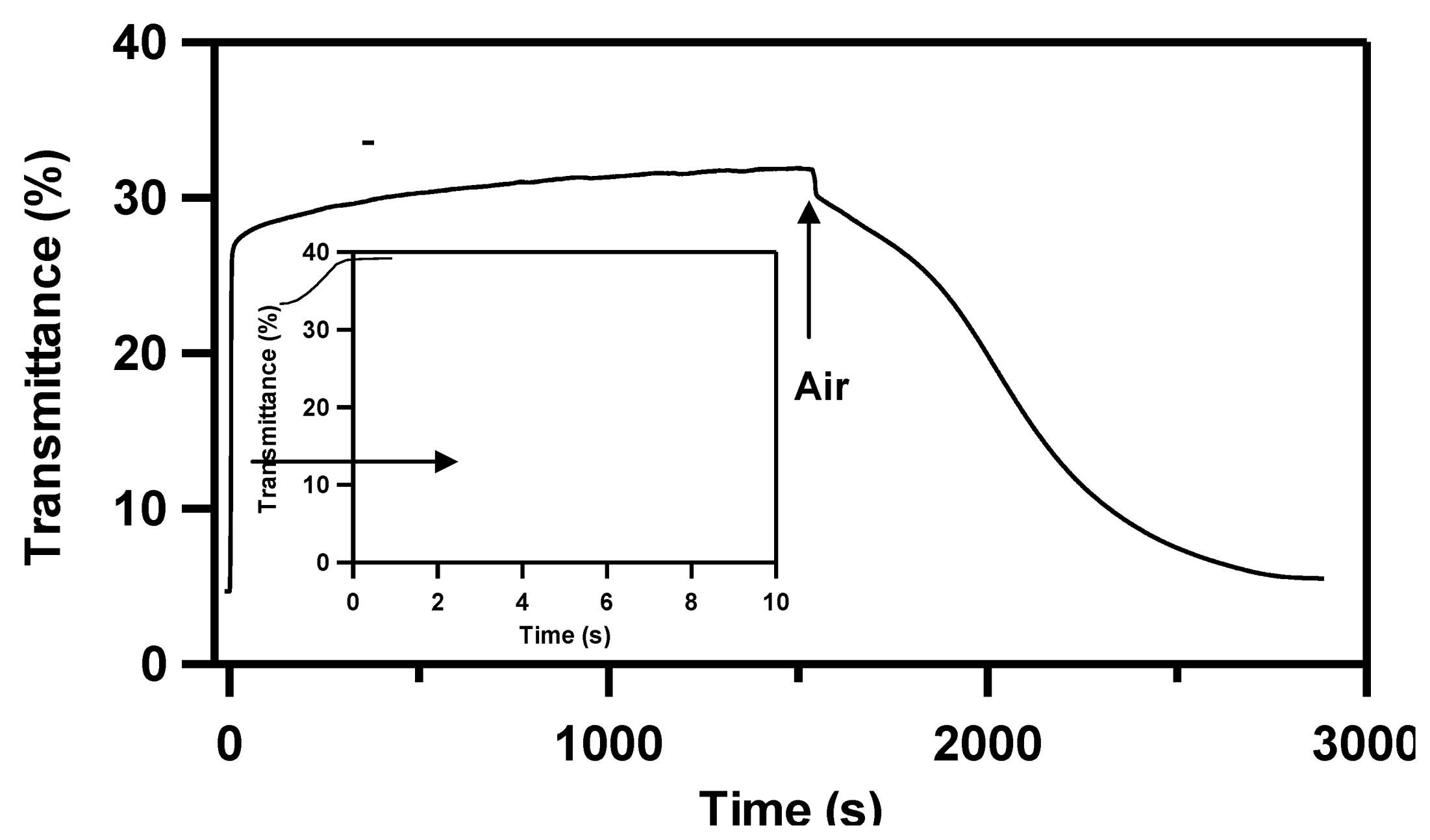
The as-deposited sample has a shiny metallic surface. An exposure to diluted H2 gas causes the drastic change from the metallic state to the transparent state by hydrogenation of Mg and the transmittance increases rapidly. Figure 1 shows the transmittance change of Pd capped Mg thin film deposited on glass substrate at room temperature. The transmittance increases from 4% to 28% in 5 seconds and then it gradually increases to 32%. After exposure to dry air, transmittance decreases gradually by dehydrogenation. The dehydrogenation process is much slower than hydrogenation and it takes about 30 minutes to return to the fully metallic state.
Figure 1.
Transmittance change of Pd capped Mg thin film after exposure of 4%H2 in Ar and air.

Upon hydrogenation, magnesium hydride (MgH2) is believed to be formed in the film. Because MgH2 is theoretically predicted to be a large band gap insulator and transparent [5], the optical transmittance is changed. Once MgH2 is formed in the film, it blocks hydrogen diffusion, which may be the reason for the slow dehydrogenation shown in Figure 1. Although the transition speed from the transparent state to the metallic state is too slow for practical use as a switchable mirror, such a rapid hydrogenation of Mg is quite interesting as a hydrogen storage phenomena. Figure 1 indicates that a considerable amount of MgH2 is formed in the film within 5 seconds at room temperature. It seems to be extraordinary fast, because the diffusion coefficient of H in Mg at 305 K is reported to be 1.1 × 10⁻²⁰ m2/s [6]. From this value it is roughly estimated to take about 500 seconds for hydrogen atom to diffuse 50 nm.
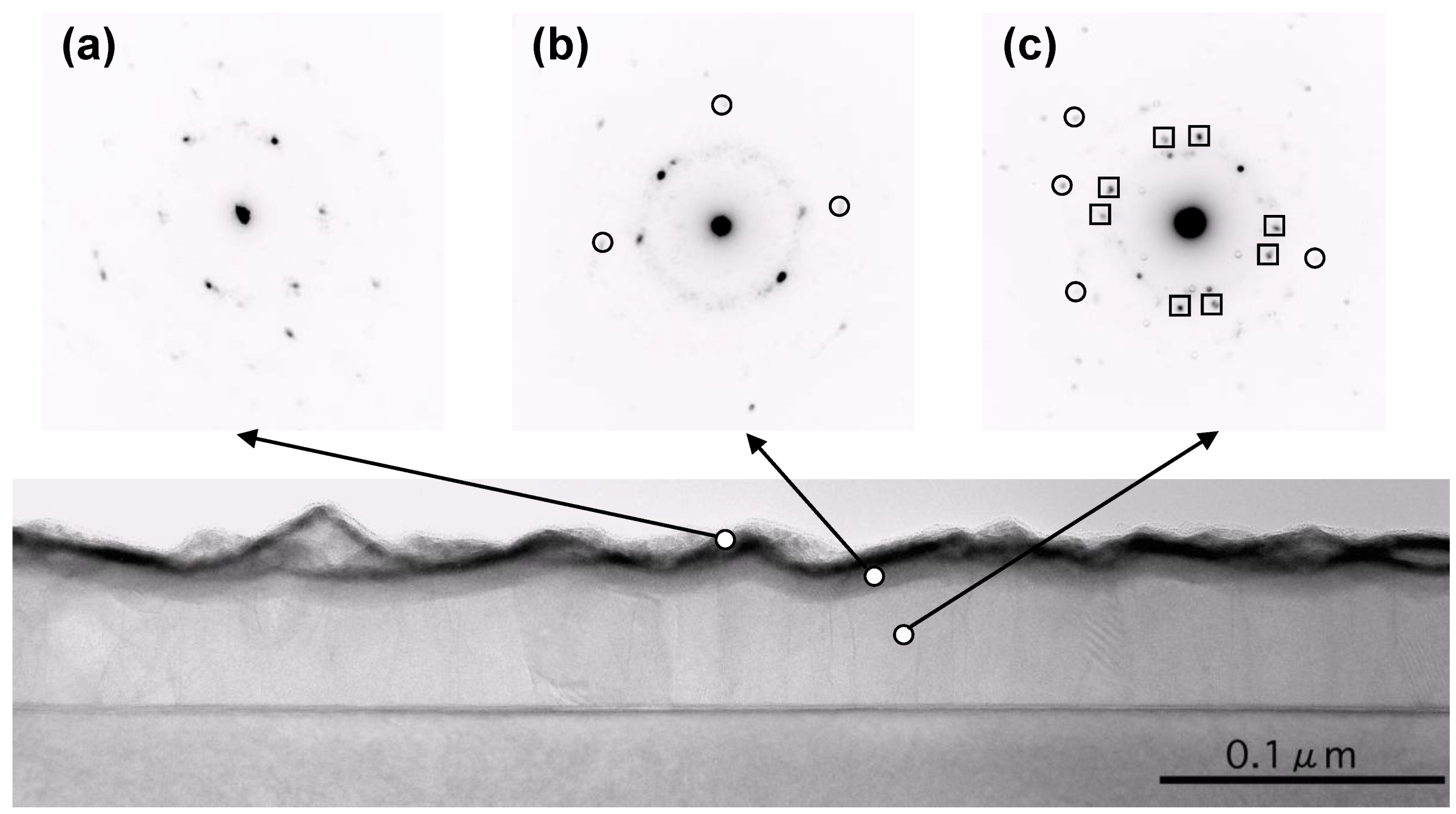
To investigate the diffusion mechanism in the film, the micro structure of Pd capped Mg thin film was characterized using TEM. Figure 2 shows the TEM image of as-deposited Pd capped pure Mg thin film deposited on Si substrate. The deposited film is clearly recognized with a total thickness of 55 nm in the image. Oxidized layer of Si substrate is also easily distinguished. The black line on the top of the film corresponds to the Pd layer. Between the Pd layer and the underlying Mg layer, a gray layer which may be a transition layer, is observed. To investigate the crystalline structure of each layer, micro diffraction patterns were taken. The micro diffraction pattern: (a) shows that Pd layer was well crystallized; In the micro diffraction pattern (b) for the transition layer, most of the spots come from Pd and spots with an open circle come from Mg; In the micro diffraction pattern (c) for Mg layer, most spots are attributed to pure Mg and some spots with open squares are attributed to MgO2. It should be noted that some other spots, which are designated by open circles in the figure, coincide with the Pd position. It means that the crystallized Pd exists even in the Mg layer.
Figure 2.
Cross-sectional image of as-deposited Pd capped Mg thin film with micro-diffraction patterns observed by TEM.
Figure 2.
Cross-sectional image of as-deposited Pd capped Mg thin film with micro-diffraction patterns observed by TEM.

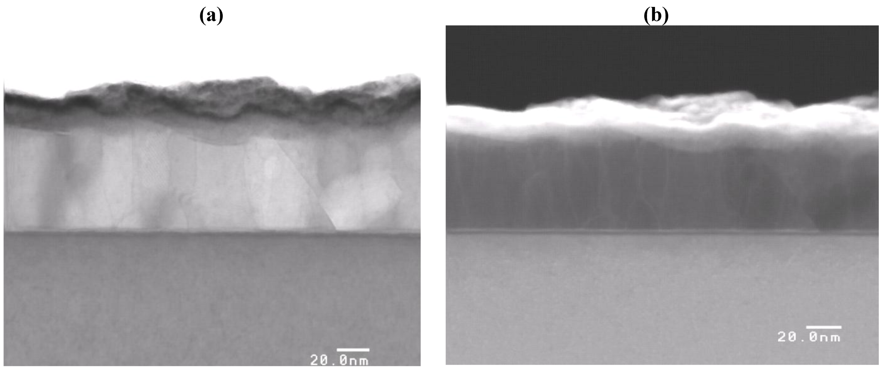
To investigate the crystalline structure of the film more precisely, STEM observation was carried out for the same sample. Figure 3a shows a middle magnification bright field image; and Figure 3b shows a HAADF (high-angle annular dark-field) image by STEM for the same sample as Figure 2. The bright field image clearly shows that the Mg layer consists of columnar grains, which is often observed for a deposited film by sputtering. A quite interesting structure is seen in the HAADF image. In this image, contrasts reflect the difference of elements and a white contrast area is supposed to consist of heavy elements; in this case Pd. We can clearly see a white area at the grain boundary. This means that Pd is distributed at the boundary of the Mg grain. In this structure it seems as if liquid Pd penetrates into the gap of Mg grain. It is curious that such a structure is formed by the subsequent deposition of Pd after Mg deposition.
Figure 3.
(a) Bright field image; and (b) HAADF image of as-deposited Pd capped Mg thin film observed by STEM.
Figure 3.
(a) Bright field image; and (b) HAADF image of as-deposited Pd capped Mg thin film observed by STEM.

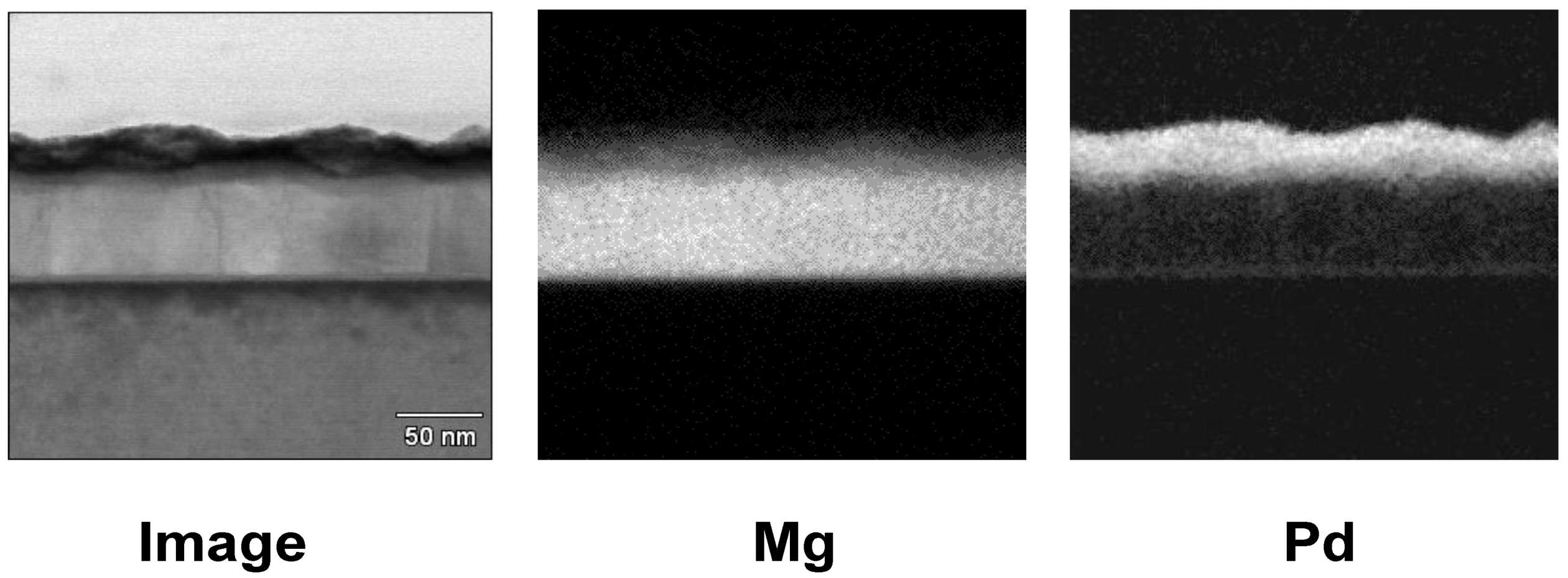
The distribution of Pd in the film is confirmed by EDX measurements. Figure 4 shows Mg and Pd distributions in the film determined by EDX using scanning electron probe of STEM for the same sample. The Pd distribution picture indicates that Pd exists at the boundary of Mg grains in the film.
These analyses show that Mg grain is surrounded by Pd in the film. This structure is extremely promising from the view point of hydrogen loading to an Mg layer, because Pd absorbs hydrogen like a sponge very quickly. So hydrogen is effectively loaded through Pd deep into the film, resulting in speedy hydrogenation as shown in Figure 1.
For the formation of this structure, Pd should be deposited immediately after Mg deposition. If the surface of Mg layer is oxidized, the hydrogenation speed of Pd/Mg thin film is reduced. This may be because Pd invasion of Mg grain is suppressed.
Figure 4.
EDX mapping of as-deposited Pd capped Mg thin film for Mg and Pd distributions.

Although the formation mechanism of the structure is not yet understood and more intense study is necessary, this anomalous structure is very interesting both from the view point of basic science and practical applications.
3. Experimental Section
Pd capped Mg thin films were deposited by DC magnetron sputtering with metal Mg and Pd targets. The detail of the preparation has been described in a previous paper [4]. Using a loadlock system, the base pressure of the deposition chamber was kept below 2 × 10⁻⁵ Pa. After evacuation, Mg thin films were deposited on a glass or Si substrate, followed by a Pd deposition. This Pd cap layer is necessary for enhancement of the hydrogen uptake kinetics and protection of the Mg layer [7].
After removal from the chamber, deposited films were exposed to 0.1 MPa 4% H2 gas diluted by Ar. The transmittance change was monitored by using a diode laser (λ = 670 nm) and a Si photodiode. The cross-sectional observation of prepared thin film was done by using 200 kV TEM (Topcon EM-002BF with STEM unit). Prior to TEM observation, the coated films are glued and sliced. After being grounded by a dimpler, the specimen was ion beam thinned to electron transparency.
4. Conclusions
Pd capped Mg thin film, with a thickness below 50 nm prepared by magnetron sputtering, can be hydrogenated very fast even at room temperature. Hydrogenation of 50 nm Mg is completed within 5 seconds. The high resolution TEM observation of Pd capped Mg thin films shows that Pd/Mg thin film has a unique structure; Pd exists at the boundary of Mg grain in the film. Such a structure is advantageous for fast hydrogen loading to the inside of Mg layer.
References
- Hydrogen in Metals, Topics in Applied Physics; Alefeld, G.; Volkl, J. (Eds.) Springer: Berlin, Germany, 1978.
- Yamamoto, K.; Higuchi, K.; Kajioka, H.; Sumida, H.; Orimo, S.; Fujii, H. Optical transmission of magnesium hydride thin film with characteristic nanostructure. J. Alloy. Compd. 2002, 330–332, 352–356. [Google Scholar]
- Yoshimura, K.; Yamada, Y.; Okada, M. Optical switching of Mg-rich Mg–Ni alloy thin films. Appl. Phys. Lett. 2002, 81, 4709–4711. [Google Scholar] [CrossRef]
- Yoshimura, K.; Yamada, Y.; Okada, M. Hydrogenation of Pd capped Mg thin films at room temperature. Surf. Sci. 2004, 566–568, 751–752. [Google Scholar]
- Yu, R.; Lam, P.K. Electronic and structural properties of MgH2. Phys. Rev. B 1988, 37, 8730–8737. [Google Scholar] [CrossRef]
- Spatz, P.; Aebischer, H.A.; Krozer, A.; Schlapbach, L. The diffusion of H in Mg and the nucleation and growth of MgH2 in thin films. Z. Phys. Chem. 1993, 181, 393–397. [Google Scholar] [CrossRef]
- Van der Molen, S.J.; Kerssemakers, J.W.J.; Rector, J.H.; Koeman, N.J.; Dam, B.; Griessen, R. Hydriding kinetics of Pd capped YHx switchable mirrors. J. Appl. Phys. 1999, 86, 6107–6119. [Google Scholar]
© 2012 by the authors; licensee MDPI, Basel, Switzerland. This article is an open-access article distributed under the terms and conditions of the Creative Commons Attribution license (http://creativecommons.org/licenses/by/3.0/).
Share and Cite
MDPI and ACS Style
Yoshimura, K. Anomalous Structure of Palladium-Capped Magnesium Thin Films. Metals 2012, 2, 253-257. https://doi.org/10.3390/met2030253
AMA Style
Yoshimura K. Anomalous Structure of Palladium-Capped Magnesium Thin Films. Metals. 2012; 2(3):253-257. https://doi.org/10.3390/met2030253
Chicago/Turabian StyleYoshimura, Kazuki. 2012. "Anomalous Structure of Palladium-Capped Magnesium Thin Films" Metals 2, no. 3: 253-257. https://doi.org/10.3390/met2030253