
Microstructures and Electrical Resistivity of Aluminum–Copper Joints

1
School of Intelligent Manufacturing, Longdong University, Qingyang 745000, China
2
State Key Laboratory of Advanced Processing and Recycling Non-Ferrous Metals, Lanzhou University of Technology, Lanzhou 730050, China
*
Author to whom correspondence should be addressed.
Metals 2023, 13(8), 1474; https://doi.org/10.3390/met13081474
Submission received: 13 July 2023
/
Revised: 8 August 2023
/
Accepted: 15 August 2023
/
Published: 16 August 2023
(This article belongs to the Special Issue Microstructure and Mechanical Property Improvement of Welded Metal Joints)
Abstract
:Using pulsed double electrode-gas metal arc welding, aluminum wires are joined to copper plates with fillers of different fractions of silicon. Two layers of different microstructures are formed near the Al-Cu interface: one consists of a hypoeutectic microstructure of α (Al) + Al2Cu, and the other consists of an intermetallic compound (IMC) of Al2Cu. Increasing the heat input causes increases in the thicknesses of the IMC layer and the layer of the hypoeutectic microstructure. Si suppresses the growth of the IMC layer and assists the growth of the layer of the hypoeutectic microstructure. The effects of the interface microstructures and chemical compositions on the electric resistivity of the joints are analyzed. The electric resistivity of the joints increases with the increase in the thicknesses of the IMC layer and the layer of the hypoeutectic microstructure. The law of mixture is used to calculate the electric resistivity of the joints, which is in accordance with the experimental results.
1. Introduction
The hybrid structure of copper (Cu) and aluminum (Al) has been widely used in a variety of applications, including the automotive [1] and aerospace industries [2] and electric power protection [3], due to the relatively low cost of the materials, the light weight of Al, its good corrosion resistance, etc. However, it is challenging to produce a high-quality joint of Al-Cu because there are huge differences in the physical properties between Al and Cu, such as the melting point and specific heat capacity [4,5]. Also, there are brittle intermetallic compounds (IMCs) formed in Al-Cu joints, which can impair the quality of the joints and increase the electric resistance [6,7,8].
There are various techniques available to join Al with Cu, including explosive welding [9,10], friction stir welding [11,12], ultrasonic spot welding [13], fusion welding [14,15], etc. Using explosive welding, Henryk et al. [10] produced an Al-Cu joint and found the IMCs of Al4Cu9, AlCu, and Al2Cu near the Al-Cu interface. Tan et al. [12] joined an 5A02 Al alloy with Cu via friction stir welding and observed the IMC layers of Al4Cu9, Al2Cu3, and Al2Cu near the interface as well as the increase in hardness associated with the IMCs. Xue et al. [16] investigated the effect of the friction stir welding parameters on the microstructures and mechanical properties of Al-Cu joints and suggested that IMCs were not necessarily detrimental to the mechanical integrity of the joints for the IMC layer with a thickness less than the critical thickness. Muhammad et al. [17] produced the Al-Cu joints using a novel ultrasonic vibration-assisted friction stir welding process. They found that, irrespective of the welding conditions (with and without ultrasonic vibrations), the intermetallic compounds were formed at the interface and the ultrasonic vibration effectively reduced the thickness of the IMC layer at the joint interface, thus improving the mechanical properties of the joints.
Fusion welding has been extensively used to join dissimilar materials, while it is very difficult to join Al with Cu using the traditional fusion welding techniques because brittle intermetallics can easily form during the cooling of the molten pool [18,19]. Generally, the heat input into base metals needs to be reduced in order to limit the formation of Al-Cu IMCs and improve the quality of the Al-Cu joints [20,21]. Using cold-metal transfer (CMT) welding to join the AA6061-T6 Al alloy to Cu, Cai et al. [14] found the IMCs of Al2Cu and AlCu in the joints, and noted the dependence of the joint strength on the size of the IMCs. Feng et al. [22] studied the effect of the heat input on the formation of IMCs in Al-Cu joints during CMT welding, and observed the IMCs of Al4Cu9, Al2Cu3, and Al2Cu near the Al-Cu interface. They found that increasing the heat input could increase the growth of IMCs, especially the Al2Cu IMC.
As both Al and Cu have high electrical conductivity, their alloys have wide applications in the electric power industry, which requires high electrical conductivity of Al-Cu joints [7]. According to previous studies, it was found that the IMCs in joints can change the electric response of Al-Cu joints. For example, Mohanraj et al. [23] carried out friction stir spot welding on the AA6061 and C11000 wires, both 2 mm in diameter; they found that the joints (0.30 to 0.34 μΩ) offered a higher range of electrical resistivity than the base metal (0.02 μΩ). Braunovic et al. [24] studied the effect of IMCs on the electrical behavior of Al-Cu joints joined via friction stir welding, and noted a linear relationship between the thickness of the IMCs and the contact resistance.
In the previous studies, various techniques have been proposed to join Al with Cu [25,26]. However, few have used a double electrode gas metal arc welding process (pulsed DE-GMAW) to join the Al wire to the Cu plate, and the microstructures and electrical resistivity of Al-Cu joints are unknown. Considering the variety of applications of the hybrid structures of Al and Cu and the potential application of fusion welding in joining Al with Cu, we used a pulsed DE-GMAW to join the Al wire to the Cu plate with fillers of different fractions of silicon and examined the microstructures and chemical compositions near the Al-Cu interface. Our work aims to investigate the microstructures and electric behavior of the Al-Cu joints manufactured through the pulsed DE-GMAW process.
2. Experimental Details
The base metals used in this work are Al wires of diameter 1.2 mm and T2 copper sheet of dimensions 200 × 50 × 2 mm3. Table 1 lists the composition of the Al wires (ER1100, ER4043, and ER4047), in which the weight fraction of Si varies in the range of 0.03 to 12.00 wt.%. The composition of T2 copper is Cu99.9Zn0.005Sn0.002Fe0.005Pb0.005Ni0.005- Sb0.002S0.005As0.002 (wt.%). The compositions for both the Al wires and the T2 copper sheet were supplied by the manufacturer. We re-examined the composition with an electron probe micro-analyzer (EPMA, Shimadzu EPMA-1600, Kyoto, Japan) and obtained the same results. The accelerating voltage was 12 kV.
Figure 1 shows the schematic of the experimental method. The Pulsed DE-GMA welding process [28,29], which is modified from metal inert gas (MIG) welding and the tungsten inert gas (TIG) welding, was used to join the Al wire to the Cu plate. The total current (Itotal) consists of the bypass current (Ibypass) and the main current (Imain) flowing into the base metal, i.e., Itotal = Ibypass + Imain. The heat input to the base metal is controlled by the bypass current. Reducing the heat input is beneficial to improve the quality of the Al-Cu joint. The Al wire was placed on the T2 copper plate during the welding. The average bypass current was 25 A, and the main currents were 45, 50, 55, 60, 65, and 70 A, respectively. The welding speed was 0.4 m/min, and the flow rate of argon was 15 L/min.
The weld bead is shown in Figure 2. Specimens (half Al and half Cu) of 30 × 3 × 4 mm3 were cut from the joints, and the thicknesses of the Al and the Cu layers were 1 mm, as shown in Figure 2b. The samples were mechanically ground and polished to achieve a mirror-like surface for the characterization of the microstructures. Optical microscopy (OM) and scanning electron microscopy (SEM) (Quanta FEG-450, FEI Company, Oregon) were used to analyze the microstructures of the joints, and energy dispersive spectroscopy (EDS) was used to determine the chemical composition near the Al-Cu interface. The cross section in Figure 2b was ground and polished for X-ray diffraction (XRD) analysis. XRD was conducted on the weld joints to identify the structures of the Al-Cu joints with the Cu Kα line on a Rigaku D/max 2500 X-ray diffraction with patterns recorded in a range of 20°~80°. The XRD analysis was conducted to determine whether the Si-based structure was formed.
A smart metal conductor resistance meter (TX-300) was used to measure the electric resistance of the Al-Cu joints; the schematic is shown in Figure 3. The positive electrode of the conductor resistance meter had two contacts, connected to the Al and Cu surface, respectively; the negative electrode was similar to the positive electrode, and the distance between the negative positive electrode was 25 mm. Using the relation between the electric resistance and electric resistivity, the apparent resistivity of the Al-Cu joints was calculated.
3. Results
3.1. Al-Cu Interface
Figure 4 shows the SEM images of the Al-Cu interface of the joints welded with three different filler wires. There are three regions, and regions Ⅰ, Ⅱ, and Ⅲ represent Cu, the transition region, and Al, respectively. The transition region is sandwiched between the base metals of Al and Cu. Two layers are formed in the transition region: one is a dense layer and the other is a loose layer. There is no observable melting zone on the side of Cu, and the interface between Cu and the dense layer is relatively straight. The thickness of the dense layer decreases with the increase in the fraction of Si, and increasing the fraction of Si leads to a more disordered structure of the loose layer. Local cracks are observed along the interface between the Cu and the dense layer for the welding with ER1100, and no cracks are observable under SEM for the welding with ER4043 and ER4047.
EDS analysis was performed to determine the chemical composition of the Al-Cu joints at different locations of A–G, shown in Figure 4. Table 2 lists the atomic fractions of the elements at the corresponding locations. Using the atomic fractions of the elements, we calculated the atomic ratio of Al to Cu. From the atomic ratio and the Al-Cu phase diagram [30], we concluded that the dense layer consists of the IMC of Al2Cu, and the other layer consists of α(Al) + Al2Cu. Si is present in both layers. The Si atomic fraction of point G was 98.1%. In all of the Al-Cu joints, we only found this Si segregation point. Therefore, we believe that this was a defect in the Al wire, which did not melt in the welding process, and formed the G point, as shown in Figure 4c.
Figure 5 shows the EDS pattern of the Al-Cu joints welded with Al wires of ER1100 and ER4047, respectively, under the action of Imain = 45 A and Ibypass = 25 A. There are two regions with a relatively uniform distribution of Cu and Al in each region, corresponding to the IMC layer and the layer of α(Al) + Al2Cu, respectively. No Si is detectable in the joint welded using the ER1100 Al wire, and Si is present in both the IMC layer and the layer of α(Al) + Al2Cu in the joint welded using the ER4047 Al wire. Such a result is in accord with that obtained from the local EDS analysis.
To check if there is a formation of Si-based structures, XRD analysis of the Al-Cu joint welded using the ER4047 Al wire with Imain = 45 A and Ibypass = 25 A was performed. Figure 6 shows the XRD patterns near both the Al and Cu sides. There is only Al2Cu present on the side of Al, and Al2Cu and Cu are present on the side of Cu. The XRD cannot detect the presence of Si near both the Al and Cu sides. Such a result suggests that there were no Si-based phases formed during the welding.
Using the SEM images, we measured the thicknesses of the IMC layer and the layer of α(Al) + Al2Cu. Figure 7a shows the thickness variation of the IMC layer with the main welding current. It is evident that the thickness of the IMC layer increases with the increase in the main electric current.
Figure 7b show the variation in the thickness of the layer of α(Al) + Al2Cu with the main welding current. It is evident that the thickness of the layer of α(Al) + Al2Cu is a linearly increasing function of the main welding current.
3.2. Electric Resistivity
Figure 8 shows the variation in the apparent resistivity of the Al-Cu joints with the main welding current. Increasing the main welding current causes an increase in the apparent resistivity of the Al-Cu joints, which is consistent with the increase in the electric resistivity of metals with the increase in temperature. Note that the Al-Cu joints welded using ER1100 have the largest nominal resistivity. The Al-Cu joints welded using ER4043 have the lowest apparent resistivity, which indicates that the Si content in the wire is not positively correlated with the resistivity of the Al-Cu joint.
4. Discussion
4.1. Al-Cu Interface
In Figure 4, the thickness of the dense layer decreases with the increase in the fraction of Si and local cracks are observed for the welding with ER1100, but no cracks are present for the welding with ER4043 and ER4047. This suggests that Si plays an important role in controlling the formation of the dense and loose layers and can limit the formation of cracks in the Al-Cu joints.
From Figure 5, we note that Cu migrated deeper into the Al matrix in the Al-Cu joints welded using ER4047 than those welded using ER1100 under the same welding conditions. This trend suggests that Si likely assists the migration of Cu in the Al matrix. Samuel et al. [31,32] studied the effect of Si on the dissolution and precipitation of the Cu-rich phase in an Al-Si-Cu alloy, and found that Si caused the decrease in the processing time of the solid solution and aging treatment. Zhang et al. [33] measured the diffusion of Cu in the α(Al) phase (Al-1.5 wt% Cu-0.4 wt%Si) and in an alloy consisting of α(Al) and Si (Al-1.5 wt% Cu-12.5 wt%Si), and noted that Cu diffused much faster in the alloy consisting of α(Al) and Si. Their results are in good accordance with the observation in this work that Si assists the migration of Cu in the Al matrix. Other scholars hold a different view. For instance, Lei et al. [20] used lap laser welding-brazing to join Al to Cu. In their study, compared with the 1.53 μm-thick IMC layer with pure Al weld filler, the thickness decreased to 0.58 μm with an Al-Si weld filler, and the Si atoms were enriched in the IMC layer. They believe that Si affected the free diffusion of the Cu atoms to the IMC layer. These differences are caused by different welding processes. Laser welding was used in the work of Lei et al. [20], while arc welding was used in this work. In the Al-Cu welding process, the effect of Si is affected by the heat input.
In the welding process, the heat input is the key factor that determines the microstructure and the performance of the joint when the composition is constant. The heat input affects the melting, material transport, and crystallization behavior, especially the composition and size of the IMC layer. The development of the IMC layer is considered to be an important factor in determining the joint integrity of the Al-Cu weld [17]. In Figure 7a, the IMC layer increases with the increase in the main electric current. As discussed by Zhou et al. [29], the growth of the IMC layer is a thermal activation process. The relationship between the thickness of the IMC layer and the welding current can be expressed as [29]
if the contribution of electron wind force is negligible. Here, a and b are constants depending on the microstructures and chemical compositions of the joints. Equation (1) is used to fit the data shown in Figure 7a, and the fitting curves with the fitting results are included in Figure 7a. It is evident that the variation in the thickness of the IMC layer with the welding current indeed follows Equation (1). The growth of the IMC layer formed in the Al-Cu joint is a thermal activation process. In the pulsed DE-GMAW process, the heat input can be reduced by increasing the bypass current, thereby controlling the thickness of the IMC layer and the cooling rate of the welding pool, as well as improving the quality of the Al-Cu joint. A lower heat input can reduce the thickness of the IMC layer and reduce the cooling rate of the weld. Therefore, we believe that the precipitation reaction of IMC will not easily occur under non-equilibrium conditions, and increasing the cooling rate is conductive to controlling the thickness of the IMC layer and improving the quality of the Al-Cu joint.
According to the fitting results listed in Figure 7a, the constants of both a and b decrease with the increase in the fraction of Si. Such a trend suggests that Si inhibits the growth of the IMC layer by increasing the migration rate of Cu in the Al matrix.
Based on the above discussion, it can be concluded that the heat input and Si content can affect the thickness of the IMC layer, thus affecting the quality of the Al-Cu joint in the pulsed DE-GMAW process. Many scholars have obtained similar conclusions by studying other welding processes.
We believe that the effect of the heat input and Si content on the IMC layer is essentially an influence on the Cu transport behavior. A low heat input causes a small amount of Cu to melt and the welding pool to solidify quickly. As a result, there is no time for the Cu atoms to transport, and there are too few Cu atoms in the molten pool, thus leading to a decrease in the IMC layer thickness of the Al-Cu joint. The influence of the Si content on the Cu transport behavior is relatively complex. In the laser welding process [20], Si could inhibit Cu transmission, and there are too few Cu atoms to form a thicker layer in the pulsed DE-GMAW process. Moreover, the heat input can be reduced by increasing the bypass current, thereby controlling the thickness of the IMC layer and the cooling rate of the welding pool, as well as improving the quality of the Al-Cu joint. In the present work, Si promoted the transport of Cu atoms, which are more uniform in the welding pool. Therefore, fewer Cu atoms result in a thinner IMC layer. In conclusion, Si could reduce the IMC layer thickness by significantly promoting or inhibiting the transport of Cu atoms.
Figure 7b shows the thickness of the layer of α(Al) + Al2Cu increases with the main welding current. The reason for such behavior is unclear; however, there are two possible reasons. First, it might be associated with the “flow” of molten Al in the joints. The “flow” of molten Al causes the formation of a “disorder” structure in the layer of α(Al) + Al2Cu. Second, the higher heat input increases the duration of the welding pool, and the Cu atoms are transferred to a larger area; as a result, the thickness of the layer of α (Al) + Al2Cu increases. In contrast to the growth of the IMC layer, Si “assists” the growth of the layer of α (Al) + Al2Cu.
4.2. Electric Resistivity
In Figure 8, the Al-Cu joints welded using ER1100 have the largest nominal resistivity. This behavior is likely due to the presence of local cracks in the Al-Cu joints (see Figure 4a), which increase the resistance to the motion of electrons. The Al-Cu joints welded using ER4043 have the smallest apparent resistivity. Such a result suggests that increasing the fraction of Si leads to an increase in the apparent resistivity of the Al-Cu joints. The above analysis indicates that if the Si content is too high or too low, both will lead to an increase in the apparent resistivity. Therefore, we can conclude that the Si content of the Al wire, which can lead to the lowest apparent resistivity of the Al-Cu joint, is between 0.03~12%.
The apparent resistivity of the Al-Cu joints shown schematically in Figure 9 can be calculated by the law of mixture, as:
where ρ, , , , and are the resistivities of the Al-Cu joints, Cu, Al, IMC, and the layer of α(Al) + Al2Cu, respectively, and L, LAl, LCu, LIMC, and Lhypo are the thicknesses of the Al-Cu joints, Cu, Al, IMC, and the layer of α(Al) + Al2Cu, respectively. For the IMC layer consisting mainly of Al2Cu, the resistivity of the IMC layer can be approximated as ~8 μΩ·cm of the resistivity of Al2Cu [24]. For the layer of α(Al) + Al2Cu, the resistivity can be approximately calculated as:
where (~49%) and (~51%) are the volume fractions of α(Al) and Al2Cu, respectively.
Using Equations (2) and (3), we calculated the nominal resistivity of the Al-Cu joints. Table 3 lists the resistivity of the base metals. Figure 10 shows the comparison of the resistivity between the measured values and the calculated values. It is evident that the calculated resistivity is compatible with the measured resistivity, which confirms the contribution of both the IMC layer and the layer of α(Al) + Al2Cu to the electric conduction of the Al-Cu joints.
A nucleus has a binding effect on electrons, and a stronger binding force could prevent the electrons from moving in a certain direction and result in greater resistance. Compared with the Al and Cu alloys, the atoms of the IMC layer are more disordered, and the atomic nucleus has a greater binding force on the electrons. Therefore, the resistance of the IMC layer is higher than that of the Al wire and Cu alloys.
It needs to be pointed out that Equation (2) only considers the contribution of microstructures to the apparent resistivity of the Al-Cu joints. As revealed in Figure 5, there are local defects/flaws present, such as crack and impurities, which can cause a change in the local resistance to the motion of the electrons and increase the nominal resistivity of the Al-Cu joints. Detailed analysis of the microstructures is needed to determine the contribution of the defects/flaws.
The above analysis shows that the electric resistivity of the Al-Cu joint is related to the microstructure. The detection of electric resistivity does not require mechanical grinding or polishing; therefore, it is easier to detect the electric resistivity than to measure the microstructure, and the microstructure can be predicted by the electric resistivity in the future.
5. Conclusions
With the potential application of fusion welding in joining Al with Cu, we have studied the effects of the welding current (heat input) and the amount of Si on the microstructures and electric resistivity of the Al-Cu joints welded using the Pulsed DE-GMA welding process. The following summarizes the results obtained in this work.
- There are two layers formed around the Al-Cu interface during welding, which are sandwiched between the base metals of Al and Cu. One layer consists of the IMC of Al2Cu, and the other consists of α(Al) + Al2Cu.
- Si suppresses the growth of the IMC layer and assists the growth of the layer of α(Al) + Al2Cu.
- Increasing the welding current causes an increase in the apparent resistivity of the Al-Cu joints. Both the IMC layer and the layer of α(Al) + Al2Cu play important roles in the electric conduction of the Al-Cu joints.
- Increasing the fraction of Si leads to an increase in the apparent resistivity of the Al-Cu joints. The microstructure of the Al-Cu joint could be predicted based on the electric resistivity in the future.
Author Contributions
Investigation, J.G., C.L. and J.B.; resources, J.G. and J.B.; writing—review and editing, J.G., J.Z. and B.G. All authors have read and agreed to the published version of the manuscript.
Funding
This work was supported by the Doctoral Fund of Longdong University (Grant No. XYBYZK2301), the Science and Technology Planning Project of Qingyang (Grant No. QY-STK-2022B-151), the Innovation Fund Project of College Teachers of Gansu Provincial Department of Education (Grant No. 2023B-206), the Science and Technology Project of Gansu Province (Basic Research Plan) (Grant No. 23JRRM737).
Data Availability Statement
The data presented in this study are available upon request from the corresponding author. The raw/processed data needed to reproduce these findings cannot be shared publicly at this time, as they are also part of an ongoing study.
Conflicts of Interest
The authors declare no conflict of interest.
References
- de Leon, M.; Shin, H. Review of the advancements in aluminum and copper ultrasonic welding in electric vehicles and superconductor applications. J. Mater. Process Technol. 2022, 307, 117691. [Google Scholar] [CrossRef]
- Paz Martínez-Viademonte, M.; Abrahami, S.T.; Hack, T.; Burchardt, M.; Terryn, H. A review on anodizing of aerospace aluminum alloys for corrosion protection. Coatings 2020, 10, 1106. [Google Scholar] [CrossRef]
- Yan, S.; Li, Z.; Song, L.; Zhang, Y.; Wei, S. Research and development status of laser micro-welding of aluminum-copper dissimilar metals: A review. Opt. Laser Eng. 2023, 161, 107312. [Google Scholar] [CrossRef]
- Bunaziv, I.; Akselsen, O.M.; Ren, X.; Nyhus, B.; Eriksson, M.; Gulbrandsen-Dahl, S. A review on laser-assisted joining of aluminium alloys to other metals. Metals 2021, 11, 1680. [Google Scholar] [CrossRef]
- Dimatteo, V.; Ascari, A.; Fortunato, A. Dissimilar laser welding of copper and aluminum alloys in multilayer configuration for battery applications. J. Laser Appl. 2021, 33, 4. [Google Scholar] [CrossRef]
- Alba-Galvín, J.J.; González-Rovira, L.; Bethencourt, M.; Botana, F.J.; Sánchez-Amaya, J.M. Influence of aerospace standard surface pretreatment on the intermetallic phases and CeCC of 2024-T3 Al-Cu alloy. Metals 2019, 9, 320. [Google Scholar] [CrossRef]
- Zoeram, A.S.; Anijdan, S.M.; Jafarian, H.R.; Bhattacharjee, T. Welding parameters analysis and microstructural evolution of dissimilar joints in Al/Bronze processed by friction stir welding and their effect on engineering tensile behavior. Mater. Sci. Eng. A 2017, 687, 288–297. [Google Scholar] [CrossRef]
- Tien, N.T.; Lo, Y.; Raza, M.M.; Chen, C.; Chiu, C. Optimization of processing parameters for pulsed laser welding of dissimilar metal interconnects. Opt. Laser Technol. 2023, 159, 109022. [Google Scholar] [CrossRef]
- Asemabadi, M.; Sedighi, M.; Honarpisheh, M. Investigation of cold rolling influence on the mechanical properties of explosive-welded Al/Cu bimetal. Mater. Sci. Eng. A 2012, 558, 144–149. [Google Scholar] [CrossRef]
- Paul, H.; Lityńska-Dobrzyńska, L.; Prażmowski, M. Microstructure and phase constitution near the interface of explosively welded aluminum/copper plates. Metall. Mater. Trans. A 2013, 44, 3836–3851. [Google Scholar] [CrossRef]
- Ouyang, J.; Yarrapareddy, E.; Kovacevic, R. Microstructural evolution in the friction stir welded 6061 aluminum alloy (T6-temper condition) to copper. J. Mater. Process. Technol. 2006, 172, 110–122. [Google Scholar]
- Tan, C.W.; Jiang, Z.G.; Li, L.Q.; Chen, Y.B.; Chen, X.Y. Microstructural evolution and mechanical properties of dissimilar Al–Cu joints produced by friction stir welding. Mater. Des. 2013, 51, 466–473. [Google Scholar] [CrossRef]
- Ni, Z.L.; Ye, F.X. Weldability and mechanical properties of ultrasonic joining of aluminum to copper alloy with an interlayer. Mater. Lett. 2016, 182, 19–22. [Google Scholar] [CrossRef]
- Cai, Z.P.; Ai, B.Q.; Cao, R.; Lin, Q.; Chen, J.H. Microstructure and properties of aluminum AA6061-T6 to copper (Cu)-T2 joints by cold metal transfer joining technology. J. Mater. Res. 2016, 31, 2876–2887. [Google Scholar] [CrossRef]
- Kraetzsch, M.; Standfuss, J.; Klotzbach, A.; Kaspar, J.; Brenner, B.; Beyer, E. Laser Beam Welding with High-Frequency Beam Oscillation: Welding of Dissimilar Materials with Brilliant Fiber Lasers; AIP Publishing: Long Island, NY, USA, 2011; pp. 169–178. [Google Scholar]
- Xue, P.; Ni, D.R.; Wang, D.; Xiao, B.L.; Ma, Z.Y. Effect of friction stir welding parameters on the microstructure and mechanical properties of the dissimilar Al-Cu joints. Mater. Sci. Eng. A 2011, 528, 4683–4689. [Google Scholar] [CrossRef]
- Muhammad, N.A.; Wu, C.S.; Tian, W. Effect of ultrasonic vibration on the intermetallic compound layer formation in Al/Cu friction stir weld joints. J. Alloys Compd. 2019, 785, 512–522. [Google Scholar] [CrossRef]
- Bergmann, J.P.; Petzoldt, F.; Schürer, R.; Schneider, S. Solid-state welding of aluminum to copper—Case studies. Weld. World 2013, 57, 541–550. [Google Scholar] [CrossRef]
- Chen, C.; Fan, C.; Cai, X.; Lin, S.; Yang, C. Analysis of droplet transfer, weld formation and microstructure in Al-Cu alloy bead welding joint with pulsed ultrasonic-GMAW method. J. Mater. Process. Technol. 2019, 271, 144–151. [Google Scholar] [CrossRef]
- Lei, Z.; Zhang, X.; Liu, J.; Li, P. Interfacial microstructure and reaction mechanism with various weld fillers on laser welding-brazing of Al/Cu lap joint. J. Manuf. Process 2021, 67, 226–240. [Google Scholar] [CrossRef]
- Yang, Z.; Fang, H.; Jin, K.; He, J.; Ge, W.; Yan, W. Modeling of microstructure evolution coupled with molten pool oscillation during electron beam welding of an Al-Cu alloy. Int. J. Heat. Mass. Tran. 2022, 189, 122735. [Google Scholar] [CrossRef]
- Feng, J.; Liu, Y.; Sun, Q.; Liu, J.; Wu, L. Microstructures and Properties of Aluminum–Copper Lap-Welded Joints by Cold Metal Transfer Technology. Adv. Eng. Mater. 2015, 17, 1480–1485. [Google Scholar] [CrossRef]
- Mohanraj, N.; Kumar, N.M.; Prathap, P.; Ganeshan, P.; Raja, K.; Mohanavel, V.; Karthick, A.; Muhibbullah, M. Mechanical properties and electrical resistivity of the friction stir spot-welded dissimilar Al–Cu joints. Int. J. Polym. Sci. 2022, 2022, 4130440. [Google Scholar] [CrossRef]
- Braunovic, M.; Alexandrov, N. Intermetallic compounds at aluminum-to-copper electrical interfaces: Effect of temperature and electric current. IEEE Trans. Compon. Packag. Manuf. Technol. Part A 1994, 17, 78–85. [Google Scholar] [CrossRef]
- Gao, P.; Zhang, Y.; Mehta, K.P. Metallurgical and mechanical properties of Al–Cu joint by friction stir spot welding and modified friction stir clinching. Met. Mater. Int. 2021, 27, 3085–3094. [Google Scholar] [CrossRef]
- Su, H.; Zhao, Q.; Chen, J.; Wu, C. Homogenizing the intermetallic compounds distribution in Al/Cu dissimilar friction stir welding joint with the assistance of ultrasonic vibration. Mater. Today Commun. 2022, 31, 103643. [Google Scholar] [CrossRef]
- Zhang, H.; Shi, Y.; Gu, Y.; Li, C. Effect of different filler wires on mechanical property and conductivity of aluminum-copper joints. Materials 2020, 13, 3648. [Google Scholar] [CrossRef]
- Shi, Y.; Shao, L.; Huang, J.; Gu, Y. Effects of Si and Mg elements on the microstructure of aluminum–steel joints produced by pulsed DE-GMA welding–brazing. Mater. Sci. Technol. 2013, 29, 1118–1124. [Google Scholar] [CrossRef]
- Zhou, X.; Zhang, G.; Shi, Y.; Zhu, M.; Yang, F. Microstructures and mechanical behavior of aluminum-copper lap joints. Mater. Sci. Eng. A 2017, 705, 105–113. [Google Scholar] [CrossRef]
- Ponweiser, N.; Lengauer, C.L.; Richter, K.W. Re-investigation of phase equilibria in the system Al–Cu and structural analysis of the high-temperature phase η1-Al1−δCu. Intermetallics 2011, 19, 1737–1746. [Google Scholar] [CrossRef]
- Doty, H.W.; Samuel, A.M.; Samuel, F.H. Factors Controlling the Type and Morphology of Cu-Containing Phases in the 319 Aluminum Alloy. In Proceedings of the 100th AFS Casting Congress, American Foundry Society, Philadelphia, PA, USA, 20–23 April 1996; pp. 20–23. [Google Scholar]
- Samuel, A.M.; Gauthier, J.; Samuel, F.H. Microstructural aspects of the dissolution and melting of Al 2 Cu phase in Al-Si alloys during sol, ution heat treatment. Metall. Mater. Trans. A 1996, 27, 1785–1798. [Google Scholar] [CrossRef]
- Zhang, D.; Peng, J.; Lan, W.; Zeng, D. Effect of silicon phase on copper diffusion speed in the Al-Si-Cu alloys. Heat Treat. Met. 2006, 31, 13–16. [Google Scholar]
Figure 1.
Experimental method: (a) Schematic of the experimental setup (The arrow indicates the direction of the current) [27]; (b) Schematic of joining process.
Figure 1.
Experimental method: (a) Schematic of the experimental setup (The arrow indicates the direction of the current) [27]; (b) Schematic of joining process.

Figure 2.
Weld bead: (a) Surface images (Imain = 45 A, Ibypass = 45 A); (b) cross section for materials characterization and electric measurement.
Figure 2.
Weld bead: (a) Surface images (Imain = 45 A, Ibypass = 45 A); (b) cross section for materials characterization and electric measurement.

Figure 3.
Schematic for the measurement of electric resistance.

Figure 4.
SEM images of the Al-Cu joints welded with different filler wires (Imain = 45 A, Ibypass = 25 A): (a) ER1100; (b) ER4043; (c) ER4047.
Figure 4.
SEM images of the Al-Cu joints welded with different filler wires (Imain = 45 A, Ibypass = 25 A): (a) ER1100; (b) ER4043; (c) ER4047.

Figure 5.
EDS pattern of the Al-Cu joints welded (Imain = 45 A, Ibypass = 25 A) with Al wires of: (a) ER1100; (b) ER4047.
Figure 5.
EDS pattern of the Al-Cu joints welded (Imain = 45 A, Ibypass = 25 A) with Al wires of: (a) ER1100; (b) ER4047.

Figure 6.
XRD patterns of the Al-Cu joint welded using ER4047 Al wire (Imain = 45 A, Ibypass = 25 A): (a) near Al; (b) near Cu.
Figure 6.
XRD patterns of the Al-Cu joint welded using ER4047 Al wire (Imain = 45 A, Ibypass = 25 A): (a) near Al; (b) near Cu.

Figure 7.
Variation of thicknesses of the IMC layer and the layer of α(Al) + Al2Cu with welding current: (a) IMC layer; (b) α(Al) + Al2Cu.
Figure 7.
Variation of thicknesses of the IMC layer and the layer of α(Al) + Al2Cu with welding current: (a) IMC layer; (b) α(Al) + Al2Cu.
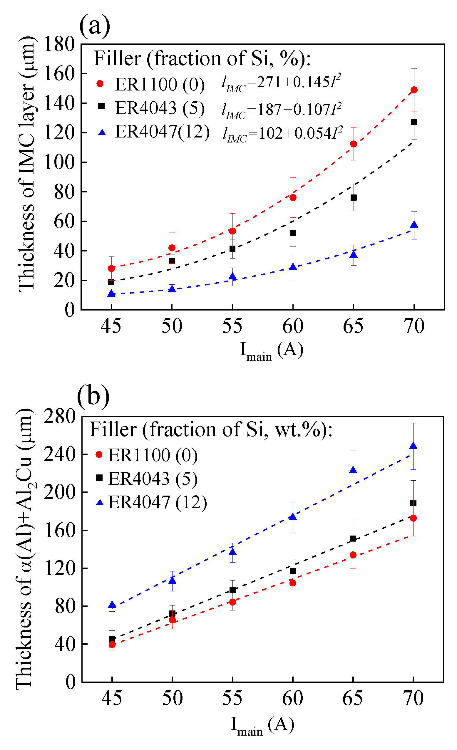
Figure 8.
Variation of apparent resistivity of the Al-Cu joints with main welding current.
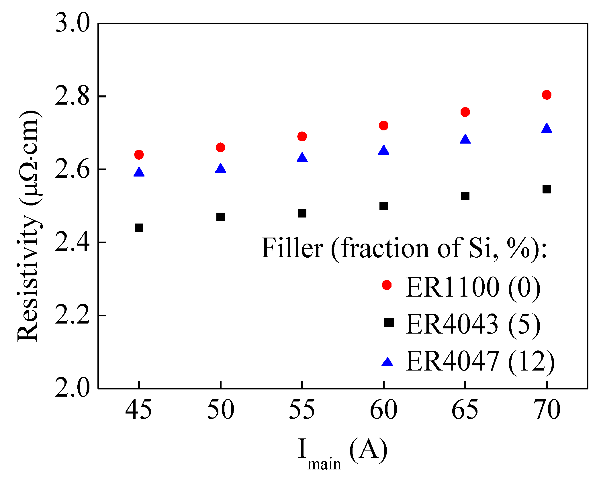
Figure 9.
Schematic for the structure of the Al-Cu joints.
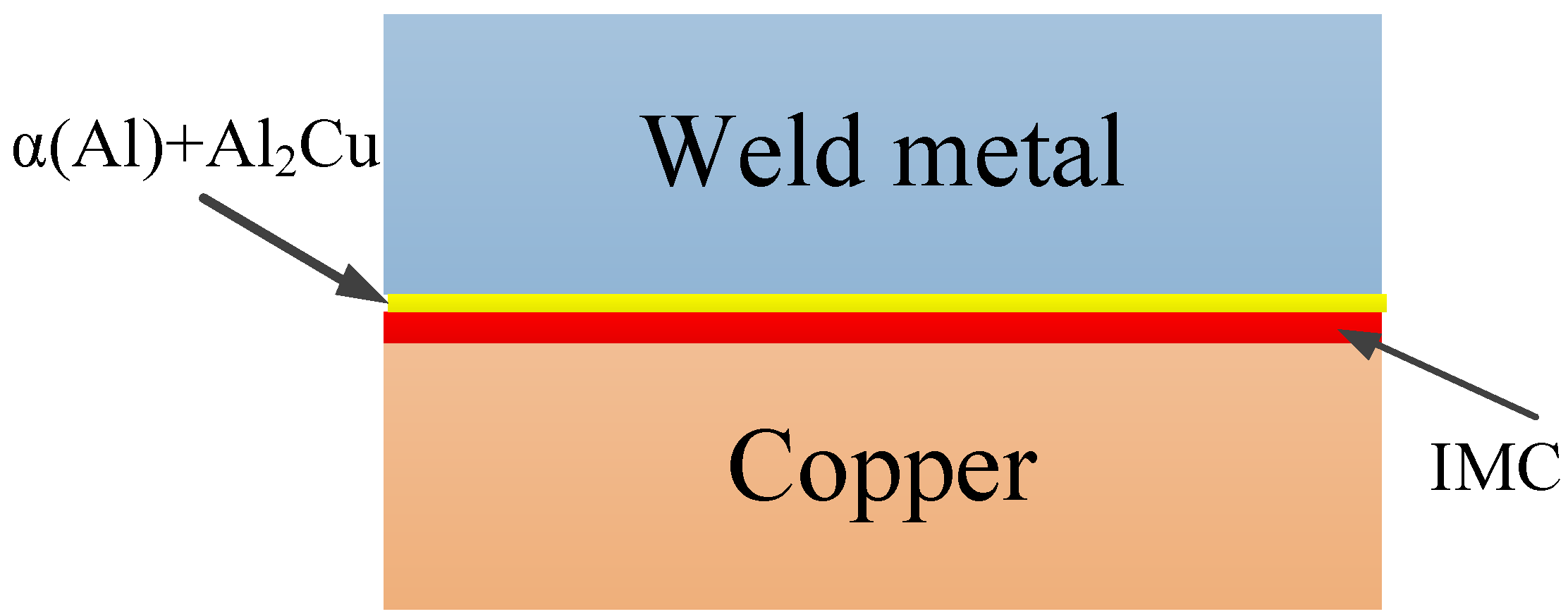
Figure 10.
Comparison of the resistivity of the Al-Cu joints.


Table 1.
Chemical composition of Al wires [27].
Table 1.
Chemical composition of Al wires [27].
| Al Wires | Si | Cu | Mg | Fe | Zn | Mn | Ti | Al |
|---|---|---|---|---|---|---|---|---|
| ER1100 | 0.03 | 0.002 | - | 0.18 | 0.013 | 0.003 | - | Bal. |
| ER4043 | 5.00 | 0.30 | 0.05 | 0.80 | 0.10 | 0.05 | 0.20 | Bal. |
| ER4047 | 12.00 | 0.30 | 0.10 | 0.80 | 0.20 | 0.15 | - | Bal. |
| Al Wires | Points | Al | Cu | Si | Possible Phase |
|---|---|---|---|---|---|
| ER1100 | A | 69.3 | 30.7 | - | Al2Cu |
| B | 82.6 | 17.4 | - | α(Al) + Al2Cu | |
| ER4043 | C | 67.7 | 32 | 0.3 | Al2Cu |
| D | 84.7 | 13.8 | 1.5 | α(Al) + Al2Cu | |
| ER4047 | E | 66.2 | 33.1 | 0.7 | Al2Cu |
| F | 83.8 | 14.6 | 1.6 | α(Al) + Al2Cu | |
| G | 1.2 | 0.7 | 98.1 | Si |
Table 3.
Average resistivity of base metals.
| Materials | ER1100 | ER4043 | ER4047 | T2 Copper |
|---|---|---|---|---|
| Resistivity (μΩ·cm) | 2.86 | 3.18 | 3.52 | 1.80 |
Disclaimer/Publisher’s Note: The statements, opinions and data contained in all publications are solely those of the individual author(s) and contributor(s) and not of MDPI and/or the editor(s). MDPI and/or the editor(s) disclaim responsibility for any injury to people or property resulting from any ideas, methods, instructions or products referred to in the content. |
© 2023 by the authors. Licensee MDPI, Basel, Switzerland. This article is an open access article distributed under the terms and conditions of the Creative Commons Attribution (CC BY) license (https://creativecommons.org/licenses/by/4.0/).
Share and Cite
MDPI and ACS Style
Guo, J.; Li, C.; Bian, J.; Zhang, J.; Geng, B. Microstructures and Electrical Resistivity of Aluminum–Copper Joints. Metals 2023, 13, 1474. https://doi.org/10.3390/met13081474
AMA Style
Guo J, Li C, Bian J, Zhang J, Geng B. Microstructures and Electrical Resistivity of Aluminum–Copper Joints. Metals. 2023; 13(8):1474. https://doi.org/10.3390/met13081474
Chicago/Turabian StyleGuo, Jinchang, Chunkai Li, Jianxiao Bian, Jianrui Zhang, and Baolong Geng. 2023. "Microstructures and Electrical Resistivity of Aluminum–Copper Joints" Metals 13, no. 8: 1474. https://doi.org/10.3390/met13081474
Note that from the first issue of 2016, this journal uses article numbers instead of page numbers. See further details here.