Article

Number Determination of Successfully Packaged Dies Per Wafer Based on Machine Vision

Photonics and Information Laboratory, Department of Electrical Engineering, National Yunlin University of Science and Technology, 123 University Road, Section 3, Douliou, Yunlin 64002, Taiwan
*
Author to whom correspondence should be addressed.
Machines 2015, 3(2), 72-92; https://doi.org/10.3390/machines3020072
Submission received: 4 June 2014 / Revised: 9 September 2014 / Accepted: 20 March 2015 / Published: 9 April 2015
(This article belongs to the Special Issue Machinery Diagnostics and Prognostics)

Abstract

:
Packaging the integrated circuit (IC) chip is a necessary step in the manufacturing process of IC products. In general, wafers with the same size and process should have a fixed number of packaged dies. However, many factors decrease the number of the actually packaged dies, such as die scratching, die contamination, and die breakage, which are not considered in the existing die-counting methods. Here we propose a robust method that can automatically determine the number of actual packaged dies by using machine vision techniques. During the inspection, the image is taken from the top of the wafer, in which most dies have been removed and packaged. There are five steps in the proposed method: wafer region detection, wafer position calibration, dies region detection, detection of die sawing lines, and die number counting. The abnormal cases of fractional dies in the wafer boundary and dropped dies during the packaging are considered in the proposed method as well. The experimental results show that the precision and recall rates reach 99.83% and 99.84%, respectively, when determining the numbers of actual packaged dies in the 41 test cases.

1. Introduction

Machine vision has been widely used in various fields because only simple devices are required, and various solutions have been proposed for different kinds of applications, such as industrial measurement [1], text recognition [2], finger recognition [3], medical image analysis [4], face recognition [5], and human computer interfaces [6]. As for the industrial measurement in a semiconductor factory, the automatic optical inspection for wafer-related processes has been widely studied in recent years, such as detecting a die in the open circuit [7], wafer defect detection [8], the LED grading system [9], and rotation calibration in wafer packaging [10].
The number of packaged dies is important information for the manufacturer. In general cases, the number of dies per wafer can be determined by existing counting algorithms [11,12,13,14], which can be found on websites [15] and [16] as well. In these methods, the number of gross dies per wafer can be estimated by entering the parameters such as wafer size, die width, die height, horizontal and vertical spacing. In Reference [11], the variables required in the proposed algorithm include the die dimensions (width and length), the size and orientation of the wafer flat, the size of the non-yielding periphery zone, and the die array relative the center of the wafer. The use and evaluation of the yield models in IC manufacturing are discussed in Reference [12]. Several die-per-wafer yield models, which are derived from Poisson, Binomial, and exponential probability density functions, are reviewed. Moreover, de Vries pointed out that there are different formulas used by different semiconductor manufacturing companies [13]. He found that the accuracy of an exact count algorithm depends on the die area and the aspect ratio. All the above methods require the input of the dimensions of the die and wafer.
Recently, computer vision based methods have received great attention in terms of detecting wafer die defects [17,18]. However, there are few studies that focus on the automatic counting of the die number in the wafer images without providing the size and dimension information for the dies and wafers. In addition to our preliminary work [19], Xu et al. proposed a wafer die-counting algorithm using the geometric characteristics [20] in the wafer images. In this work, RANSAC (Random Sample Consensus) algorithms [21,22] are used to detect the wafer location and the sawing lines. The incomplete dies at the wafer rim strip containing the circle pixels can be easily detected and are then eliminated. Both high counting accuracy and good computational efficiency can be achieved. However, this method does not deal with cases of fractured and randomly dropped dies on the wafer.
In practical situations, some situations that could lead to incorrect counting results should be considered. For example, with the IC testing programs, some dies in a wafer that do not pass the test will not be packaged. The dies not being packaged are left on the wafer and thus a number of dies that different from those successfully packaged are obtained. General commercial equipment [23] could automatically calculate the number of dies in the above case. However, in the cases of the remaining dies that are broken, displaced, or rotated, they cannot be determined straightforwardly. Thus a manual calculation is required if the actual number is desired. It is very time consuming to obtain the precise number of successfully packaged dies through manual wafer inspection. This number should be exactly the same as that determined from the pick and place robot. The clients of the die-packaging factory can only estimate the number, assuming that no abnormal cases occurred during the process. However, this number is usually less than that of actual packaged dies. If the difference between the two numbers is large, the clients will not accept the result and will ask for an explanation. Therefore, in this study we propose a computer-vision-based method that can automatically determine the exact number of actual packaged dies in the residual wafer image. As opposed to existing methods, the wafer and die parameters such as size, width, and length are not required. In addition, the determined die-per-wafer number can be more accurate when abnormal cases occur during the packaging process.
The remaining part of the paper is organized as follows. In Section 2, the proposed methods with the required image processing algorithms are described. The experimental results are provided in Section 3. Finally, the conclusions are drawn in Section 4.

2. Method

Figure 1 shows the systematic block diagram of the proposed system, which consists of five stages in order to determine the number of packaged dies per wafer: (1) wafer region detection: detect the actual wafer region from the input image; (2) wafer position calibration: calibrate the rotation angle of the input wafer image; (3) die region detection: detect the packaged die region from the wafer region; (4) detection of die sawing lines: determine vertical and horizontal segmentation lines in the wafer region, and then use them to partition off the rectangular die regions; (5) die number counting: determine the exact number of actual packaged dies. The detailed procedures are described in later subsections.
Figure 1. The system flowchart of the proposed method.
Machines 03 00072 g001

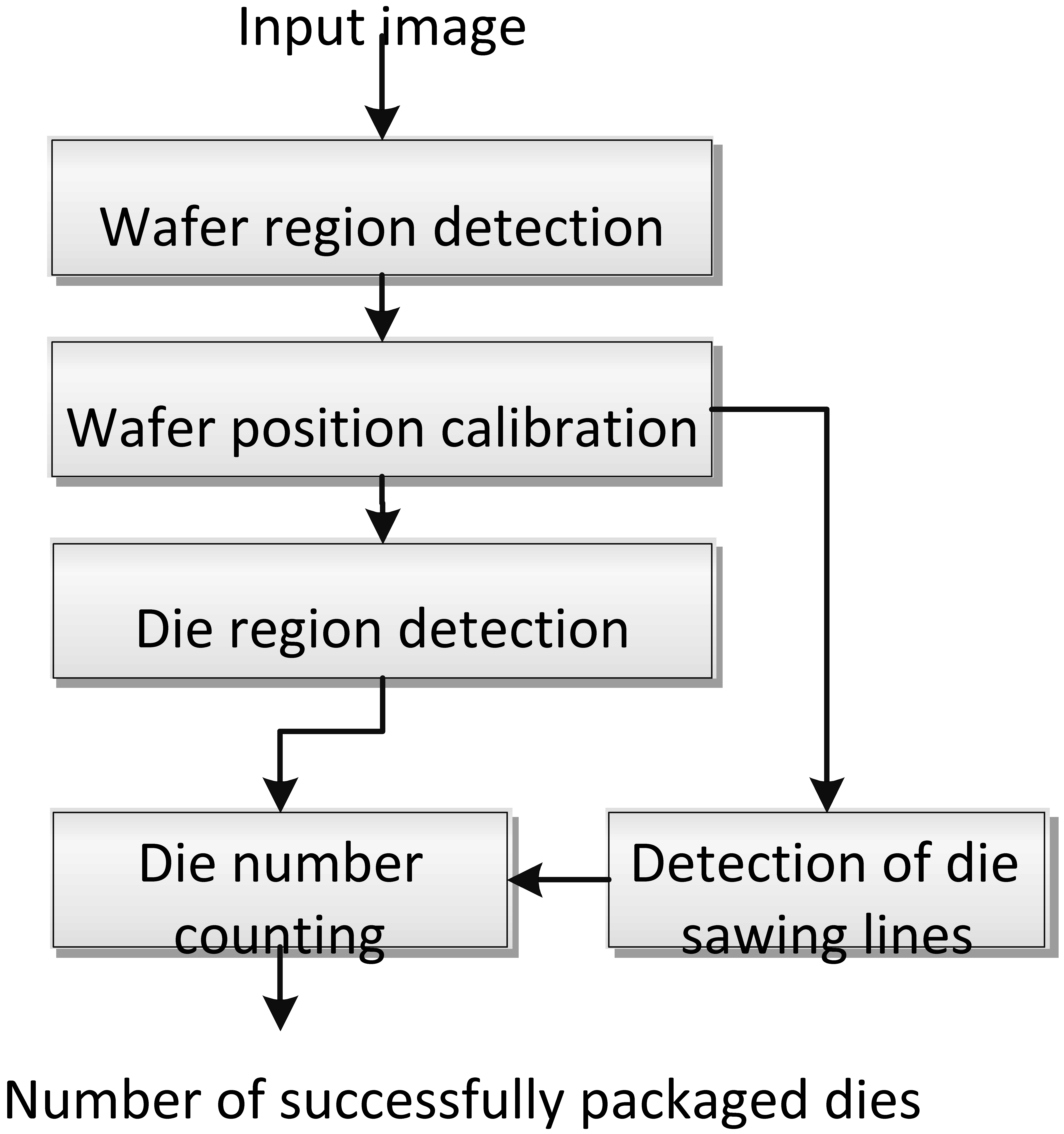
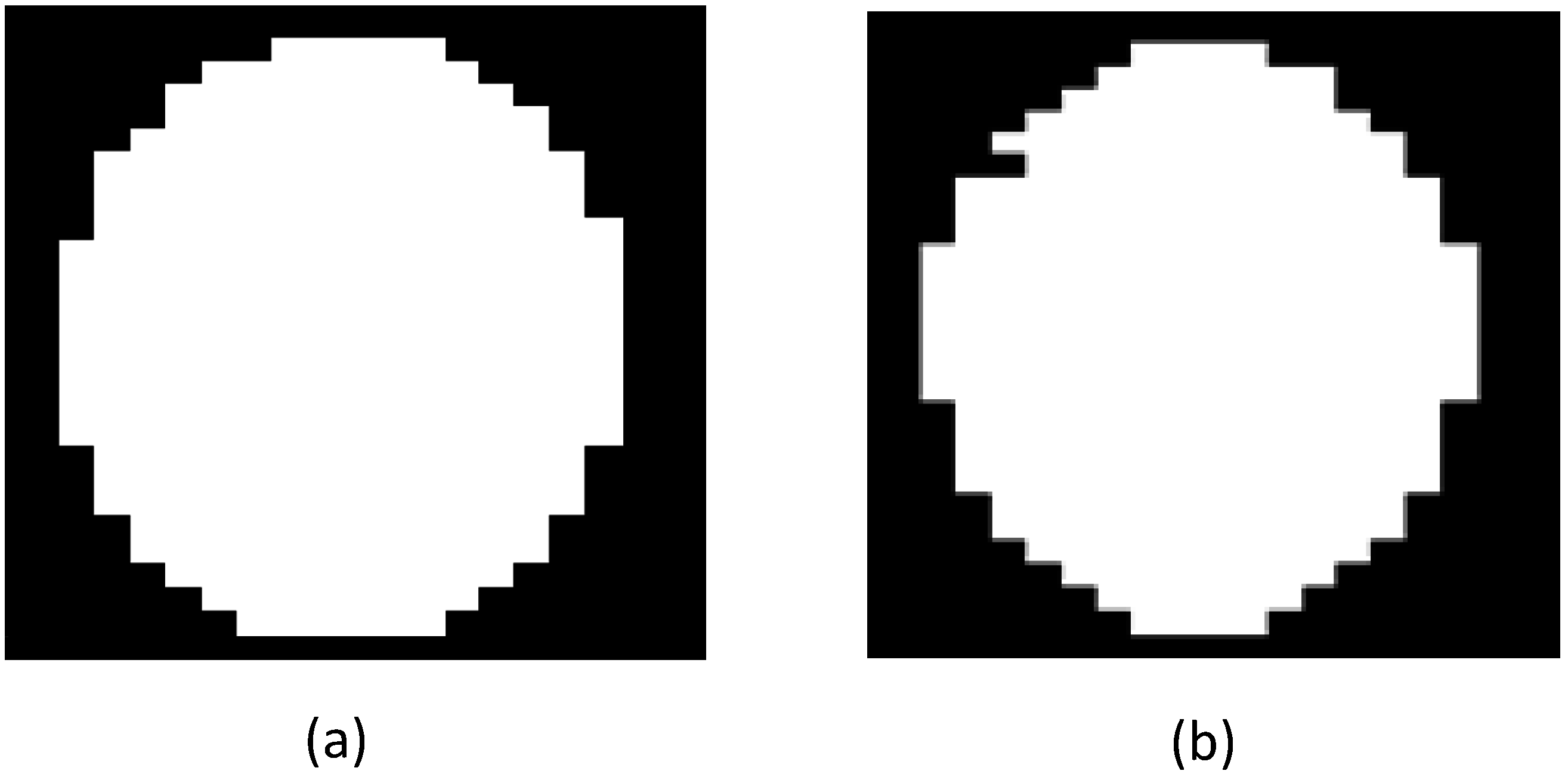
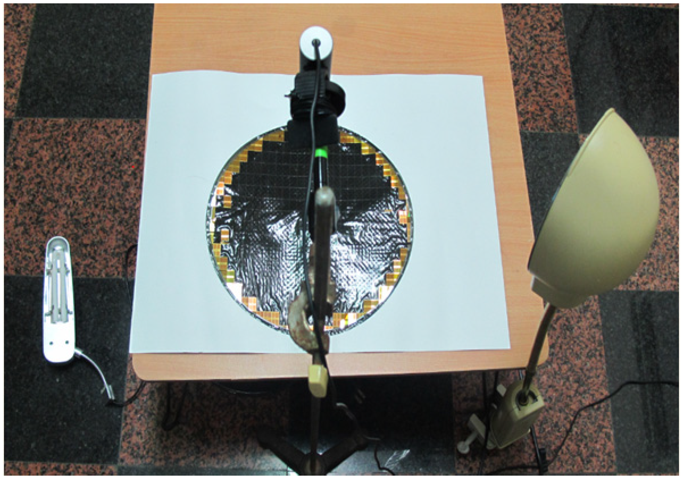
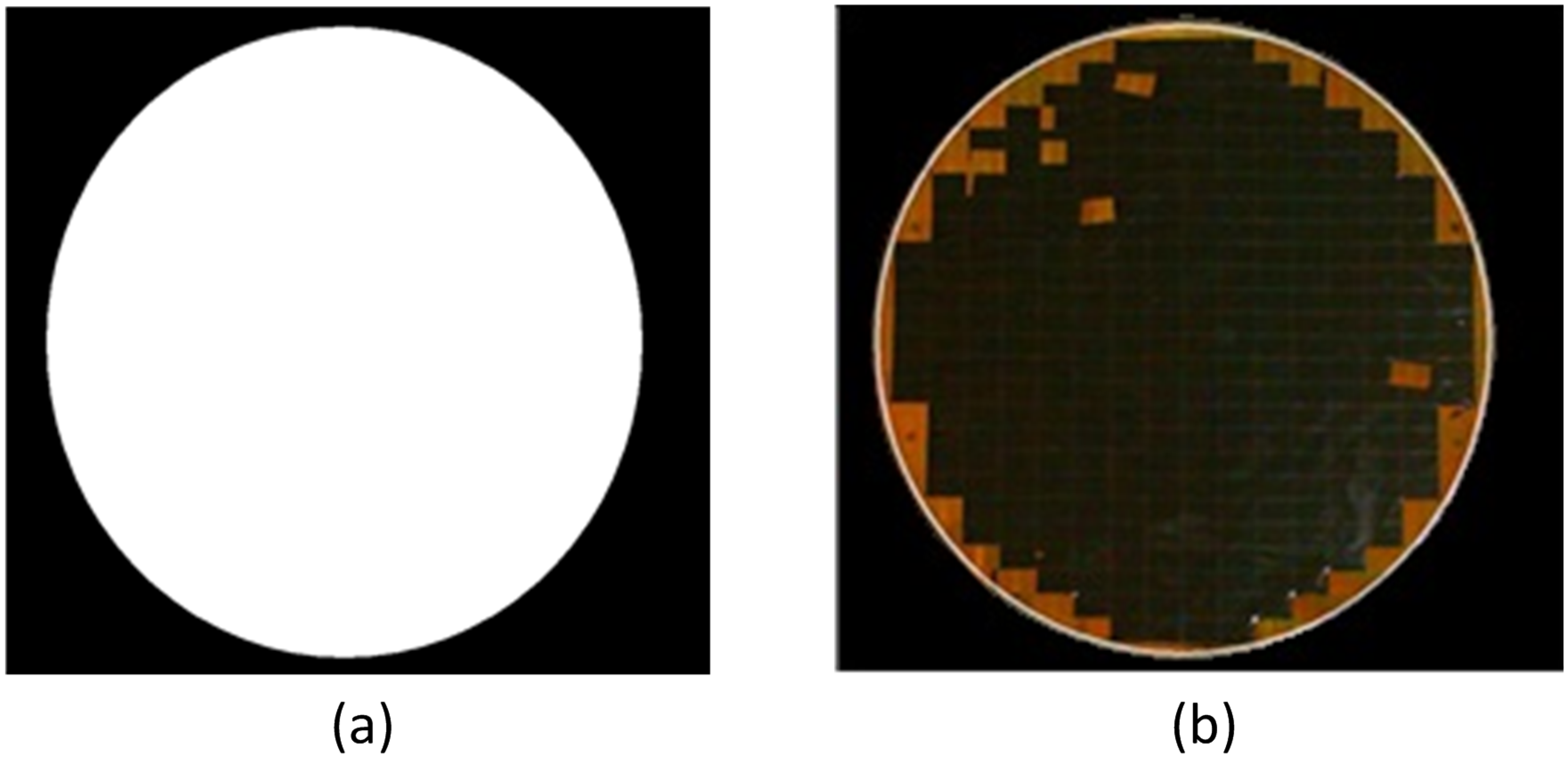
2.1. Wafer Region Detection

Figure 2a shows the input wafer image, which has redundant background information that should be removed for further processing. The detailed steps include: (1) color to grayscale transformation and binarization; (2) region labeling; (3) position calibration.
Figure 2. (a) Original image; (b) grayscale image; (c) histogram of the grayscale image; (d) binarized image.
Machines 03 00072 g002

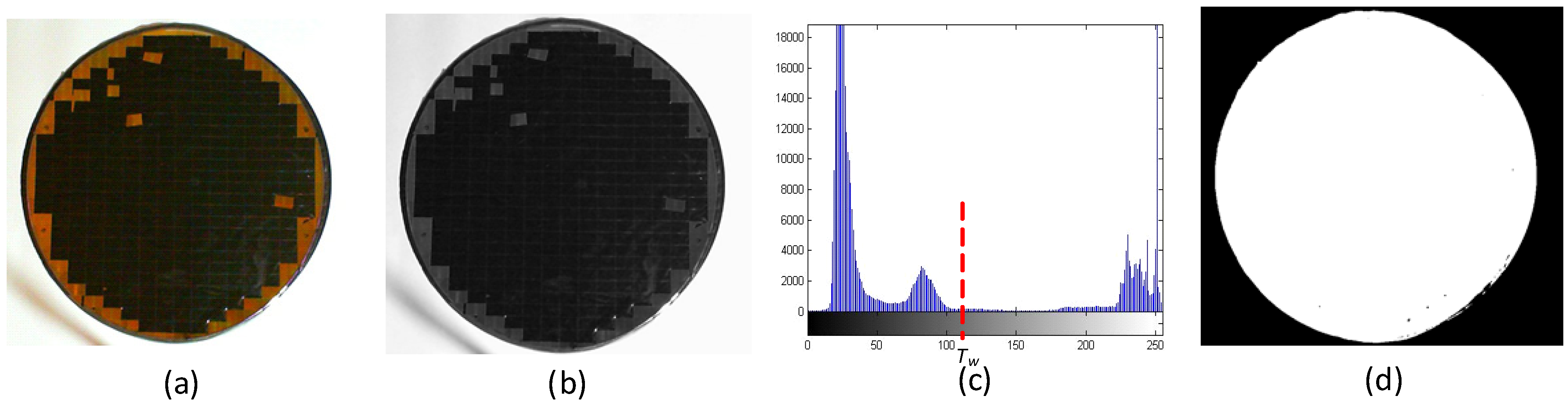
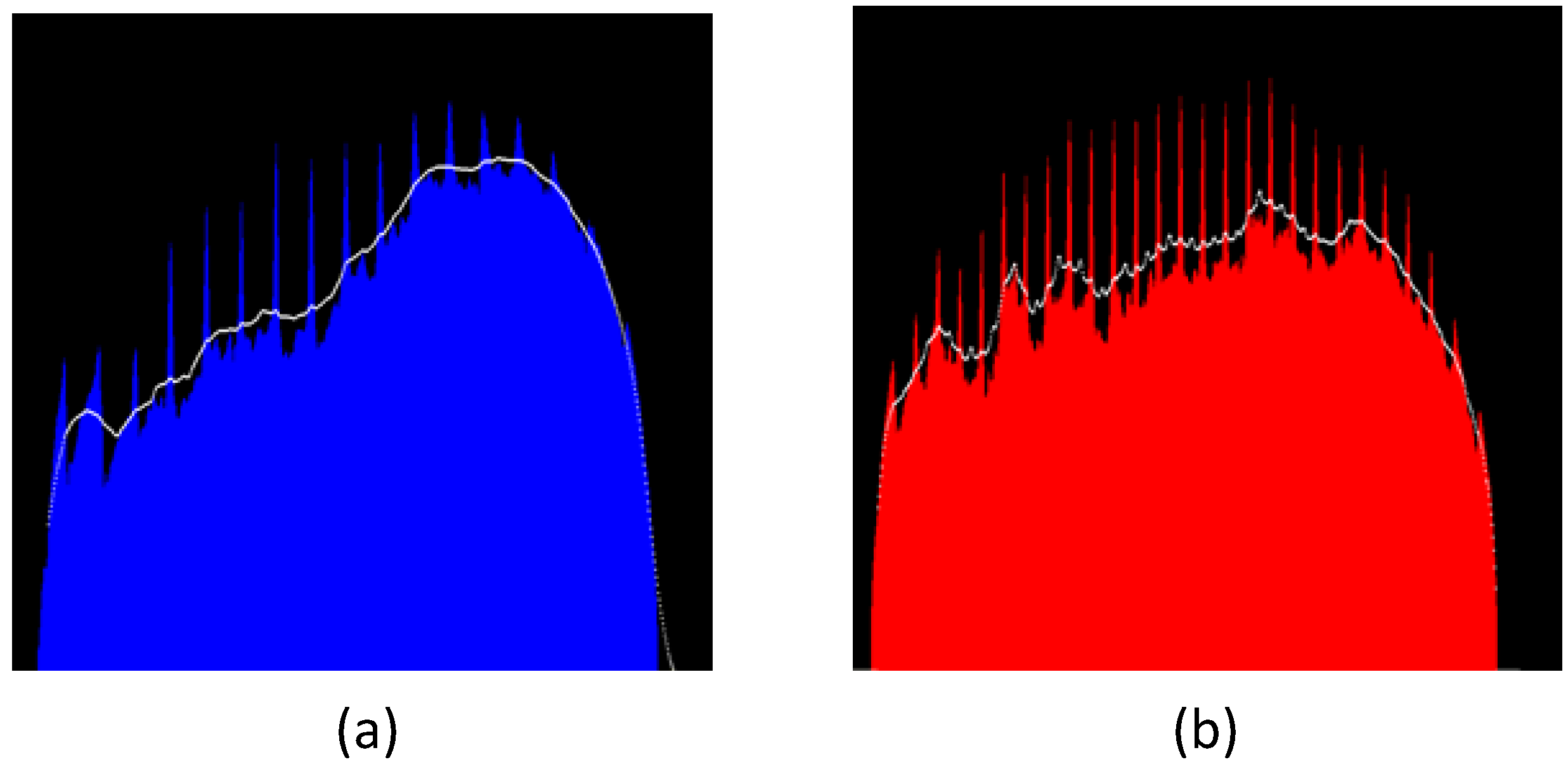
2.1.1. Color-to-Grayscale Transformation and Binarization

A color image is composed of red, green, and blue components. Each component has a one-byte resolution, i.e., 256 grayscale levels. A color image can be transformed to a grayscale image i gray ( x , y ) by using the linear combination method shown in Equation (1).
i g r a y ( x , y ) = 0.299   ×   i r ( x , y )   +   0.587   ×   i g ( x , y )   +   0.114   ×   i b ( x , y )
where ir, ig, and ib denote the grayscale values in red, green, and blue components, respectively, and (x,y) denotes the pixel coordinates.
The binarization process is often used in the object detection and segmentation framework in image processing. The main idea is to select a threshold Tw and to force all the pixel values into two fixed grayscale values, 0 and 255, as shown in Equation (2).
w b ( x , y ) = { 0 ,   if   i gray ( x , y ) > T w         255 ,   Otherwise  
where wb(x,y) is the pixel value after binarization. Figure 2b shows the grayscale image transformed from Figure 2a. Figure 2c shows the histogram of the image in Figure 2b. The threshold TW can be automatically determined by applying Otsu’s method [24] on the histogram of the grayscale image. Figure 2d shows the binarized result of Figure 2b, based on Equation (2). The white wafer region is well extracted from the black background.

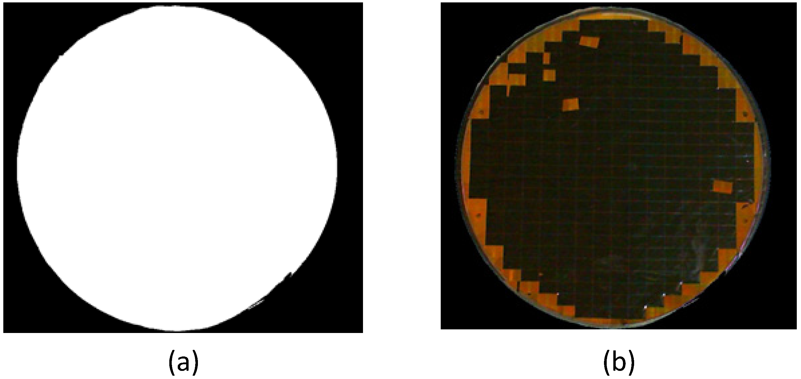
2.1.2. Region Labeling

In order to remove the background and keep the wafer information simultaneously, the mask must conform to the sharpness of the wafer. In Figure 2d, there are certain small regions (black points) in the white region boundary and they should be removed. The connected component labeling method [25] is used to determine the small black regions and the size of each region. Only the largest black area can be retained with the operation shown in Equation (3).
w b ( x , y ) = { 0 ,   if   w label ( x , y ) = t         255 ,   Otherwise    
where t is the label of the maximum black region and w label is a matrix that denotes the labeling result. Figure 3a,b show the mask w b and the final wafer image w without the background information, respectively. As shown in Equation (4), the final wafer image is obtained as passing the input wafer image onto the mask w b , i.e.,
w ( x , y ) = i ( x , y )     w b ( x , y )
Figure 3. (a) The mask of capturing the wafer image; (b) Wafer image with black background.
Machines 03 00072 g003

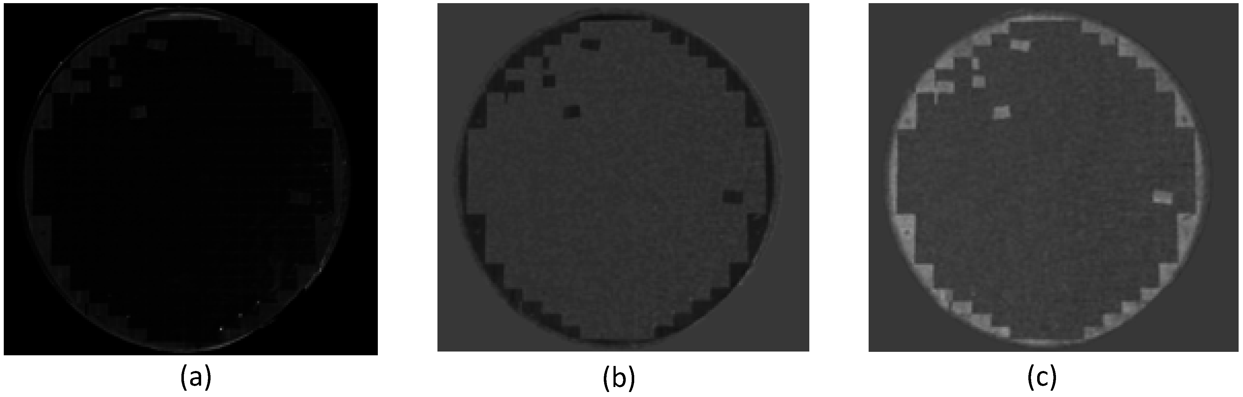
2.2. Wafer Position Calibration

Due to the possible deviation on the wafer placement, the die sawing lines could not be exactly horizontal and vertical in the image, which is necessary in order to accurately determine the die number in the following processing steps. Here, the Canny edge detection [26] and Fourier transform methods are used to determine the wafer rotation angle. First, a Canny edge detector is utilized to obtain the edge information w e ( x , y ) in the wafer image shown in Figure 3b. Figure 4a shows that many horizontal and vertical sawing lines appear in this image. This edge information can be transformed into the frequency domain We(u,v) by using the two-dimensional Fourier transform shown in Equation (5).
W e ( u , v ) = w e ( x , y ) e j 2 π ( u x + v y ) d x d y
Figure 4b shows the corresponding spectrum image, W e ( u , v ) , in which the major components appear at the nearly horizontal and vertical directions. In order to determine the angle θ rotated from the exact horizontal and vertical axes, the threshold Tc shown in Equation (6) is used to binarize the spectrum image W e ( u , v ) . Figure 4c shows the binary image C t ( u , v ) derived from the image shown in Figure 4b.
C t ( u , v ) = { 0 ,   if   W e ( u , v ) > T c         255 ,   Otherwise  
To determine the rotation angle of the wafer, two points C t ( u h , v h ) and C t ( u l , v l ) located on the points in the nearly vertical direction in the image C t ( u , v ) are selected. By using Equation (7), the deviation angle θ can be determined as
θ = π 2 t a n 1 ( v h v l u h u l )
The deviation angle θ can be used to calibrate the wafer image w ( x , y ) such that the sawing lines are as perfectly horizontal and vertical as possible. Equation (8) shows that the new coordinates (x’, y’) of the rotated image W’(x’, y’) can be determined from the coordinates (x,y). However, if the coordinates (x’, y’) are non-integers, the bilinear interpolation is utilized to obtain the integer coordinates. Figure 5 shows the rotated image after using the position calibration.
[ x y ] = [ c o s  θ c o s  θ s i n  θ   s i n  θ ] [ x y ]
Figure 4. (a) Canny edge detection result of Figure 3b; (b) spectrum of the edge image shown in Figure 4a; (c) binary image in which the black points are corresponding to strong white points shown in Figure 4b.
Machines 03 00072 g004
Figure 5. The wafer-region image after the position calibration.
Machines 03 00072 g005

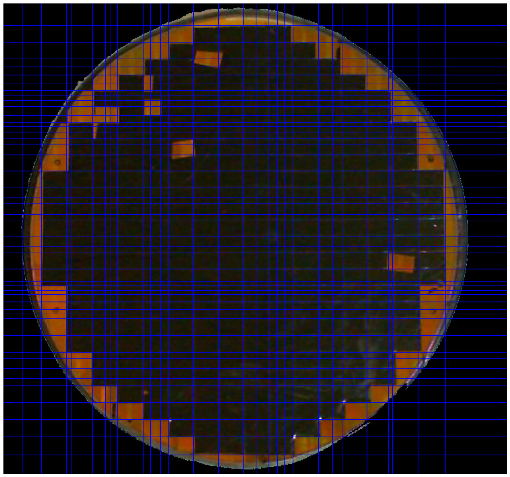
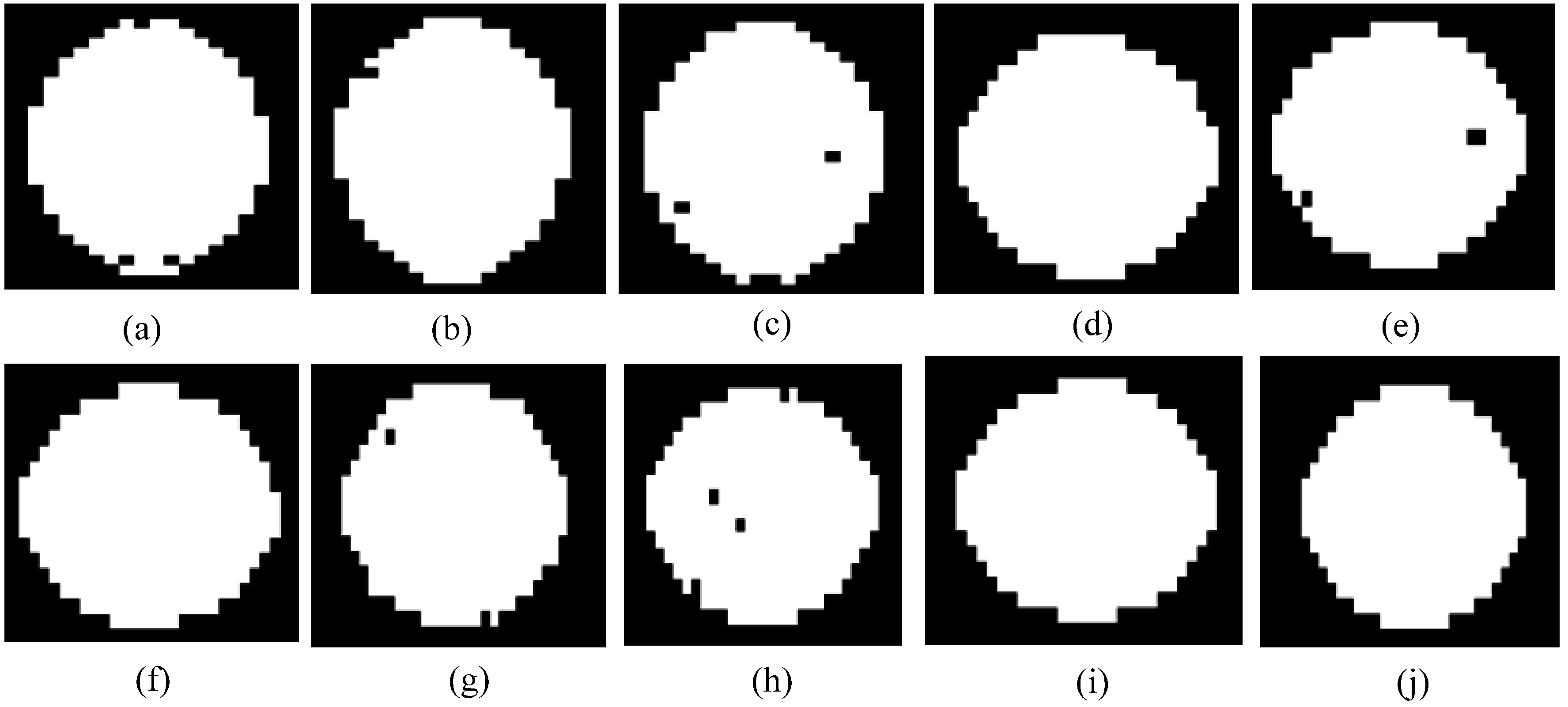
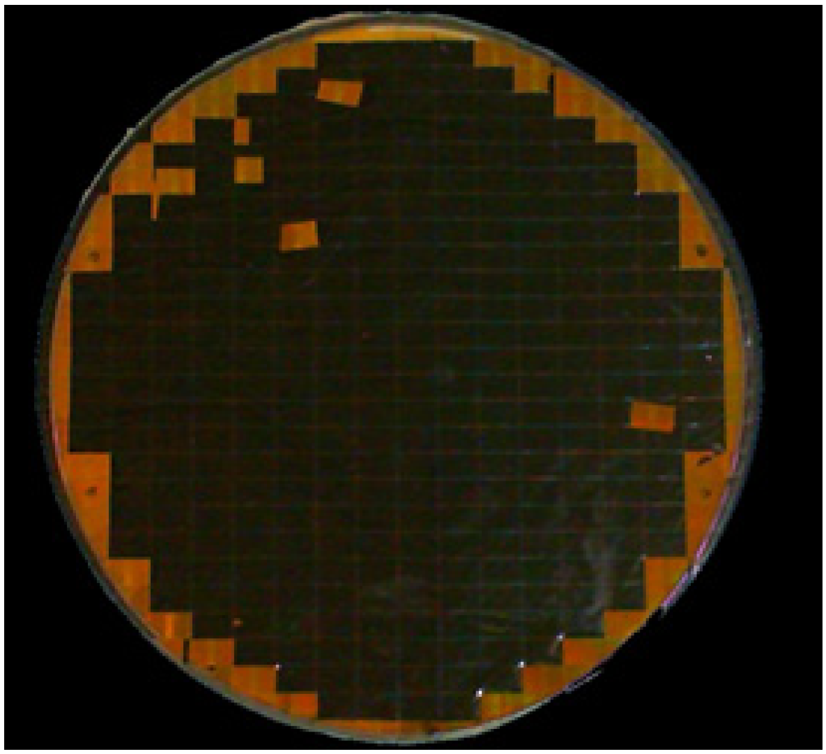
2.3. Die region Detection

After the wafer region has been determined and its position has been calibrated in Subsection 2.2, the resident die regions, which are not taken away during packaging, are detected. In order to avoid the color saturation problem caused by the reflective points in the RGB color space, the YCbCr color space is utilized such that the brightness can be separated from its color components. Equation (9) shows the transformation function.
[ Y C b C r ] = [ 16 128 128 ] + [ 65.481 128.553 24.966 37.797 74.203 112 112 93.786 18.214 ] [ R G B ]
Figure 6a–c show the Y, Cb, and Cr components of the wafer image in Figure 5, respectively. As shown in Figure 6b, the Cb component has a more obvious contrast than the other components and is nearly unaffected by reflection. To extract the regions of the resident dies, a binarization process defined in Equation (10) is used.
W dies ( x , y ) = { 255 ,   if   C b ( x , y ) < T c b           0 ,   Otherwise  
where Cb(x,y) denotes the pixel value in the Cb component, Tcb is the threshold value, which is determined by applying Otsu’s method on the histogram of the Cb component image shown in Figure 7a; and W dies ( x , y ) denotes the resident die image shown in Figure 7b.
Figure 6. (a) The Y component image; (b) the Cb component image; (c) the Cr component image in the YCbCr color space.
Machines 03 00072 g006
Figure 7. (a) Histogram of the Cb component; (b) the image of the resident die regions.
Machines 03 00072 g007
As shown in Figure 5, the rim strip of the wafer contains no dies and should be excluded to avoid possible confusion on die counting in further processing. In the third step, the area of the wafer region which does not include the rim strip is determined. The four non-zero value points (xa,ya), (xb,yb), (xc,yc), and (xd,yd) corresponding to the top, bottom, leftmost, and rightmost boundary points, respectively, are selected in the image W dies shown in Figure 7b. The four points can be used to define an ellipse mask region W D using Equation (11).
W D ( x , y ) = { 255 ,   if   ( x h ) 2 α 2 + ( y k ) 2 β 2 1 0 ,   Otherwise    
where
h = x a + x b 2 ,   k = y a + y b 2 ,   α = x d x c 2 ,   β = y a y b 2
Figure 8a shows a typical mask region, which is very close to a circle. By applying this mask onto the image in Figure 5, Figure 8b shows that the mentioned rim strip (shown in the white region) can be successfully removed.
Figure 8. (a) The mask of the wafer image; (b) the wafer image in which the region outside the white contour has been removed.
Machines 03 00072 g008

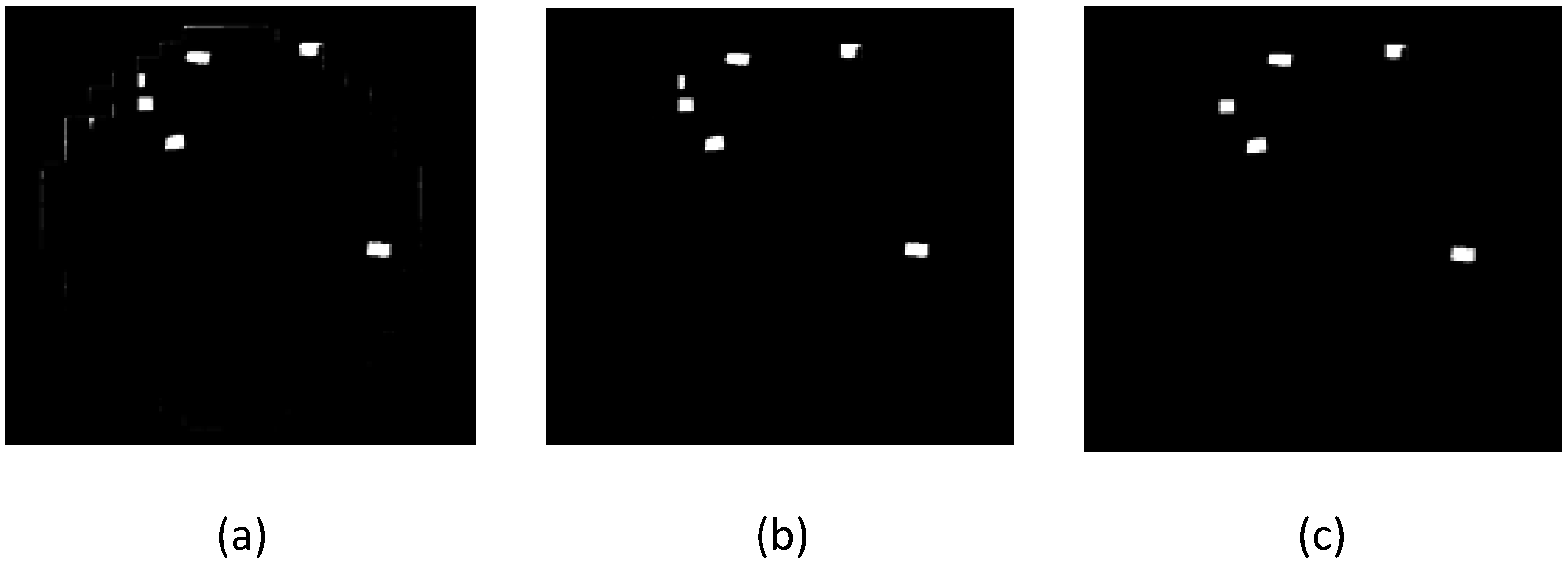
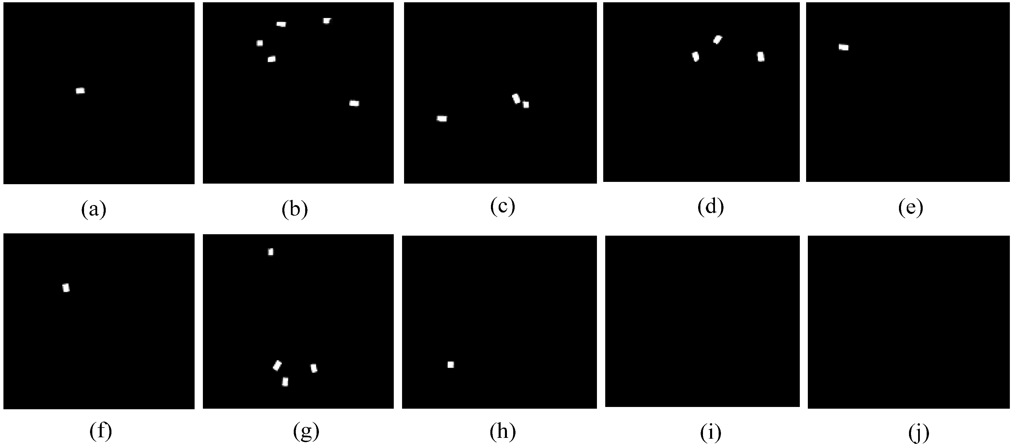
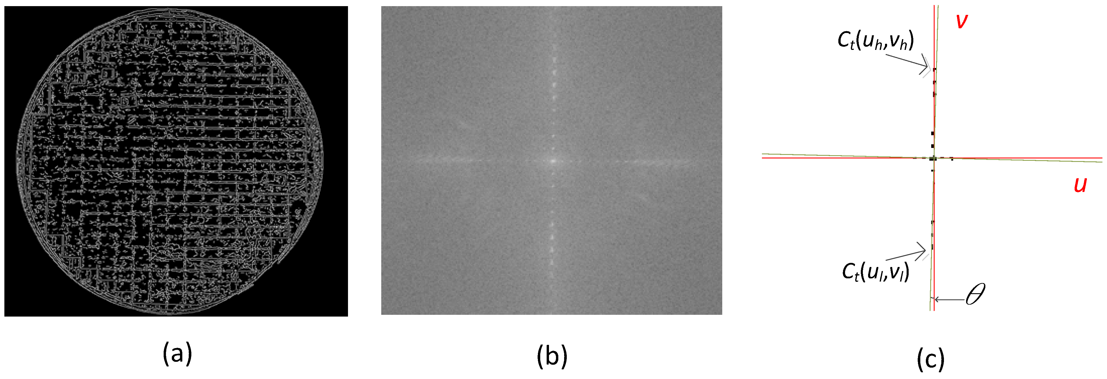
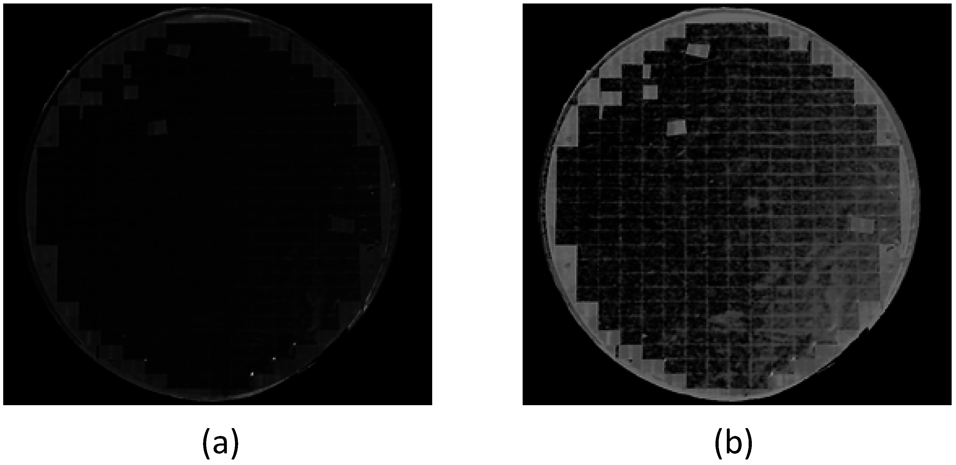
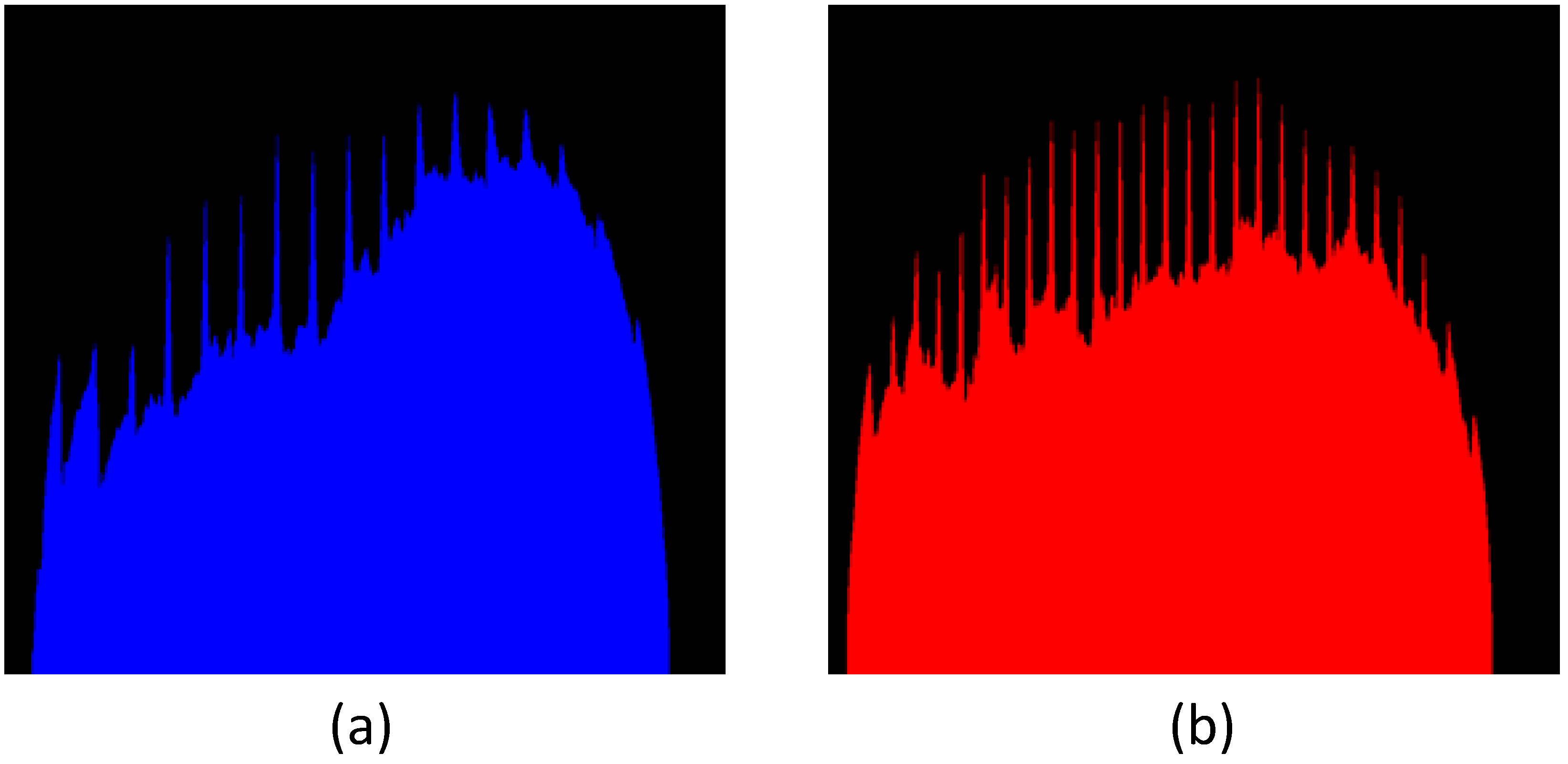
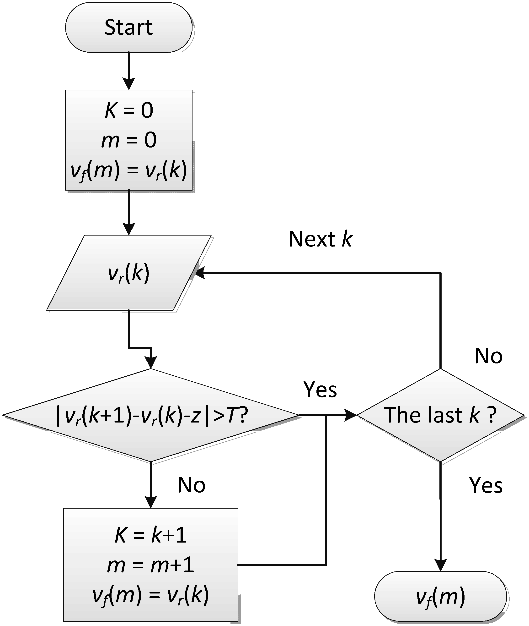
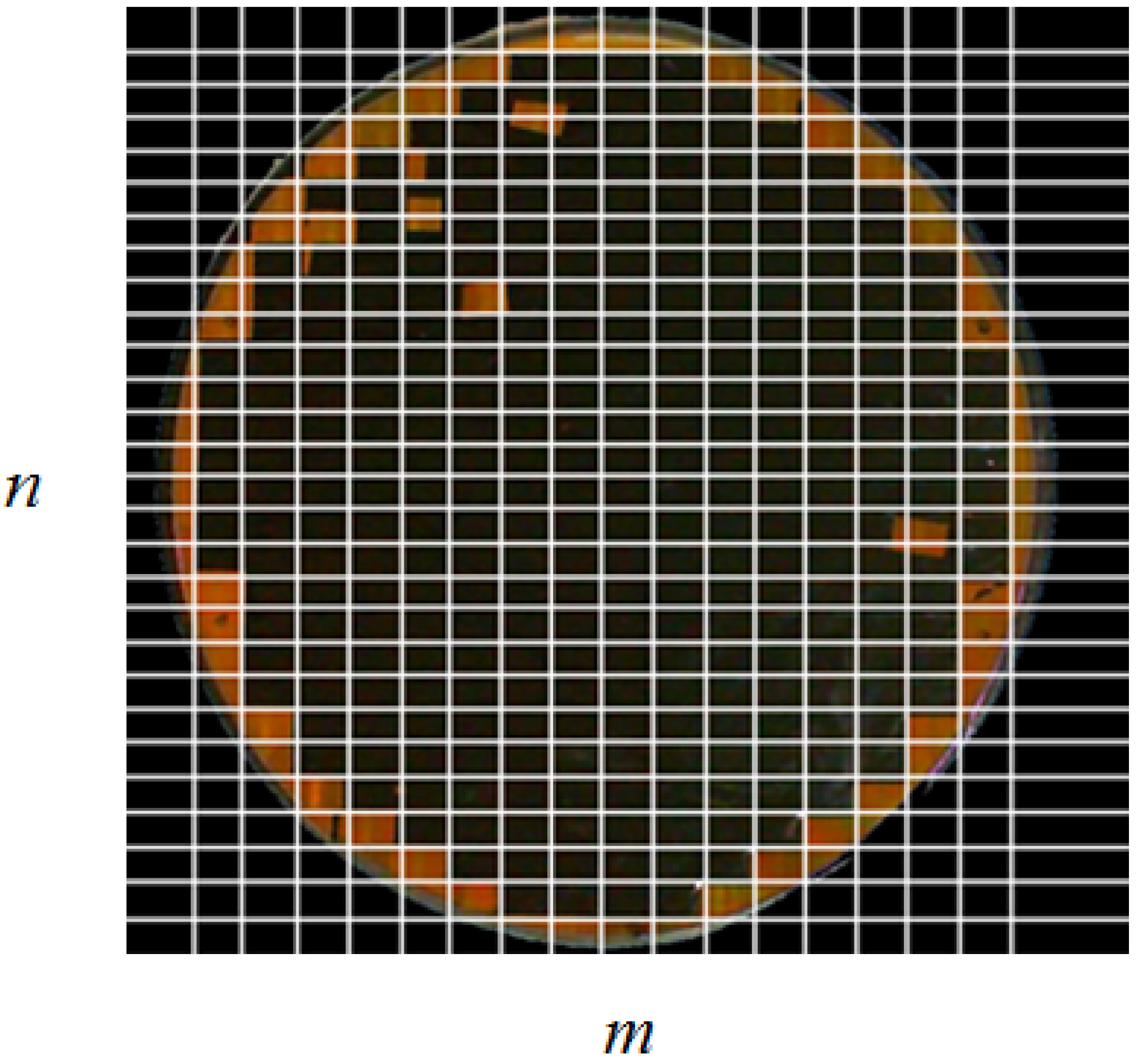
2.4. Detection of Die Sawing Lines

Prior to die counting, the geometrical information of a standard die, whose shape is rectangular and is defined by the sawing lines, should be derived. Therefore, detecting the die sawing lines in the wafer image is required. However, the sawing lines shown in Figure 9a are not obvious and thus are difficult to be easily detected. To overcome this problem, the histogram equalization method that can increase the global contrast in the image [27] is used. Figure 9b shows the enhanced result of Figure 9a. In this enhanced image e ( x , y ) , the sawing lines have been intensified, thus they can be more easily detected. Equations (12) and (13) show that the pixel values of each column and row in the wafer image (Figure 9b) are accumulated to obtain the two vectors v ( j ) and h ( i ) , respectively.
v ( j ) = x e ( x , j )
h ( i ) = y e ( i , y )
Figure 9. (a) The grayscale image obtained from Figure 3b; (b) the enhanced image e(x, y) obtained by applying the histogram equalization on Figure 9a.
Machines 03 00072 g009
Figure 10a,b show the projections of the accumulated pixel values in the columns and rows, respectively. In both projections, many obvious peaks appear in accordance with the sawing line positions in the wafer image shown in Figure 9b, because the pixel values in the sawing lines are much larger than that in the die regions. In addition, the intervals between two consecutive peaks should be very similar in these two projections. However, due to the incomplete dies and the non-uniform illumination condition, the peak and non-peak values vary a lot. Therefore, the peaks cannot be detected by directly applying a fixed thresholding scheme. Figure 11 shows the flowchart of the proposed method to detect the peak positions vp(j) in the vertical direction. Here j denotes the index of the detected peaks. The peak positions hp(i) in the horizontal direction can be detected with a similar strategy.
Figure 10. The projections of the accumulated values in (a) the columns and (b) the rows.
Machines 03 00072 g010
Figure 11. Peak detection flowchart in the vertical direction.
Machines 03 00072 g011
Figure 12 shows the detected die sawing lines in both the vertical and horizontal directions. The peak detection method described above shows that many incorrect sawing lines are detected. To solve this problem, the average line method is proposed to filter out the miss-detected sawing lines. Figure 13a,b show the depicted white lines representing the average values calculated by using Equations (14) and (15), respectively.
v ( j ) = j l j + l v ( j ) + v ( j ) l + 2
h ( i ) = i z i + z h ( i ) + h ( i ) z + 2
where v and h are the average values in the sliding windows of widths. Assume that l and w are the length and width of the die when the threshold T shown in Figure 11 is increased to a larger number in the peak detection method, respectively. As shown in Figure 11, a larger threshold T indicates a higher difference values between the two consecutive bins in the histogram. Figure 14a shows the detected peak positions with a large T value. The values l and z are calculated by using Equations (16)–(19), where we define the shortest distant between two peak positions to be length and width of the die in the histogram with a T value.
l = m i n ( D h ( i ) )
z = m i n ( D v ( j ) )
D v ( j ) = v p ^ ( j + 1 ) v p ^ ( j )
D h ( i ) = h p ^ ( i + 1 ) h p ^ ( i )
where v p ^ and h p ^ denote the detected peaks positions. D v and D h denote the distances between two consecutive peak positions in the vertical and horizontal directions, respectively. The die sawing lines vp and hp detected in the peak detection method are compared to the average values v and h , respectively. If the condition vp (j) > v ( j ) is satisfied, the new die sawing line is recorded as vr(k) = vp(j). Figure 14b shows the detection result based on this average line method.
Figure 12. Result of the die sawing line detection.
Machines 03 00072 g012
Figure 13. The result of the average line method: (a) average values shown on a white line in the vertical direction; (b) average values shown on a white line in the horizontal direction.
Machines 03 00072 g013
The last step is to guarantee that the distance between the adjacent real wafer saw lines vr(k) and vr(k+1) is greater than a predefined value z. Figure 15 shows the flowchart of this process and Figure 16 shows the final result of the die sawing lines.

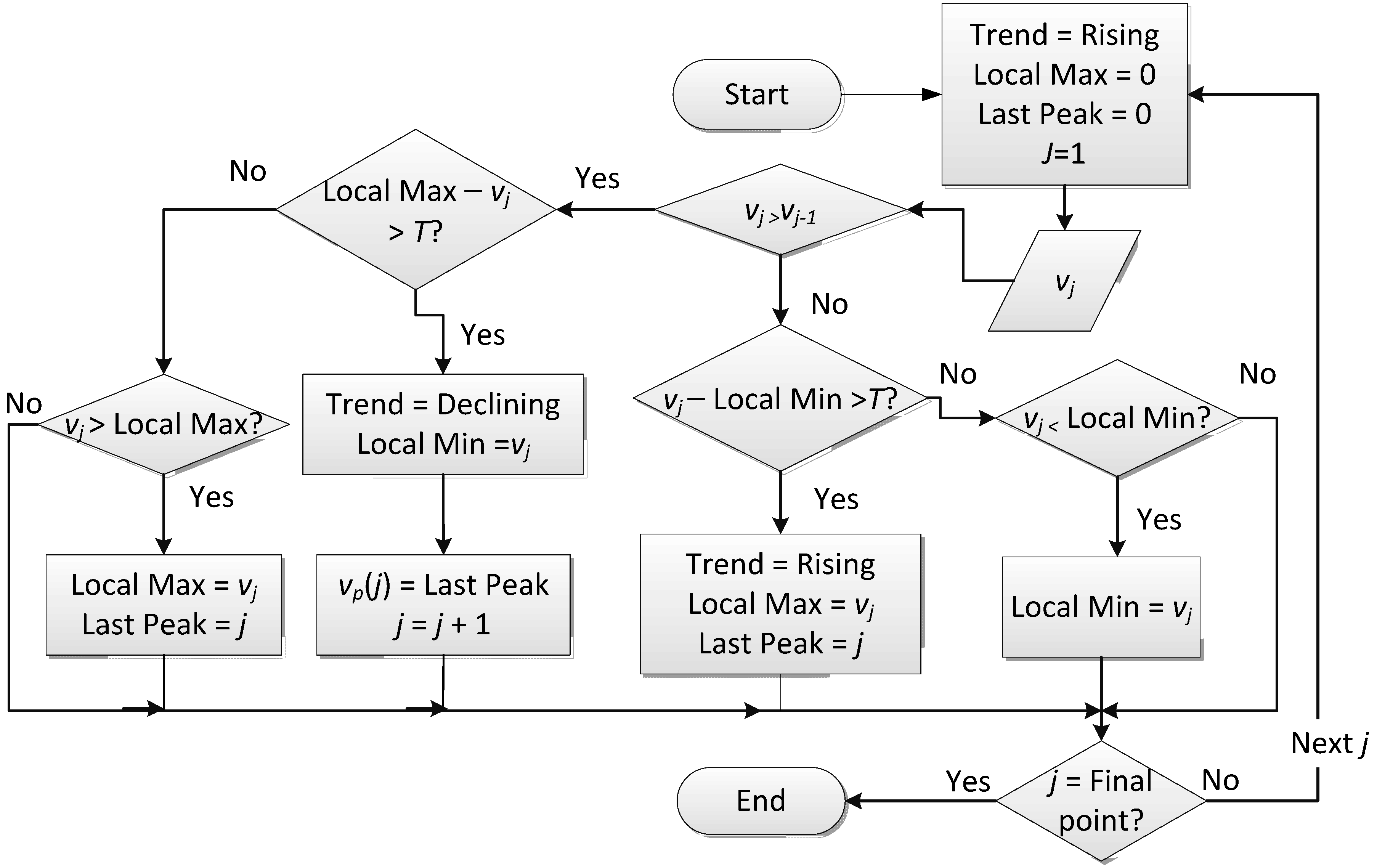
2.5. Counting the Packaged Dies Number

With the detected die sawing lines shown in Figure 16, the exact number of successfully packaged dies can be determined. In a normal case, the dies that have been taken away from the wafer can be determined. In special cases, some dies are broken, rotated, or displaced during the wafer sawing, wafer probing, or packaging processes. In counting the number of regular rectangular dies, both the normal and special cases must be considered.
Figure 14. (a) The result of the peak detection method with a T value; (b) the result of the average line method.
Machines 03 00072 g014

2.5.1. Normal Cases

Figure 17 shows that a matrix is constructed based on the die sawing lines. The binary entry value of the matrix is determined using Equation (20). The main idea is to evaluate the size of the wafer image W D in each corresponding local area, N c ( m , n ) and to use the threshold T n 1 for judging whether the die in this location has been packaged or not.
N c ( m , n ) = { 1 ,   if   x = v f ( m ) v f ( m + 1 ) y = h f ( n ) h f ( n + 1 ) W D ( x , y ) 255 > T n 1   0 ,   Otherwise
where the coordinate (x,y) denotes the pixel position in the image, the coordinate (m,n) denotes the entry position in the matrix, and Nc denotes the area corresponding to the size of dies shown in Figure 18a. Some special dies, which should be taken away but in fact are not, or the opposite case, are also considered here. The information of the resident die image Wdies is utilized to identify the actual die number N in the normal case. Equations (21) and (22) show the steps to determine the number N. Figure 19b shows the resultant image in which the incomplete dies have been discarded.
N c ^ ( m , n ) = { 1 ,   if   N c ( m , n ) = 1   and   x = v f ( m ) v f ( m + 1 ) y = h f ( n ) h f ( n + 1 ) d ( x , y ) 255 < T n 2 0 ,   Otherwise
N = m n N c ^ ( m , n )
where T n 2 is the threshold used to judge the location of the die which has been packaged or not, N denotes the number of the packaged dies in the normal case, and d ( x , y ) denotes the calibrated wafer image shown in Figure 5.
Figure 15. The flowchart of the last step.
Machines 03 00072 g015
Figure 16. The final result of the detected die sawing lines.
Machines 03 00072 g016
Figure 17. Wafer image mapped in the matrix defined by using the detected die sawing lines.
Machines 03 00072 g017
Figure 18. (a) The area that is judged to be packaged; (b) actual packaged area in the normal case.
Machines 03 00072 g018

2.5.2. Abnormal Cases

If the resident dies are broken, rotated, or shifted from the normal position, they are abnormal cases, and should be treated in another way. Consider the calibrated wafer image shown in Figure 5. First, the intersection of the calibrated image and the actual packaged die image shown in Figure 18b is determined. The dies belonging to the abnormal case can be determined using Equation (23).
S a ( x , y ) = d ( x , y ) N c ^ ( x , y )
where S a denotes the image of the abnormal case shown in Figure 19a. It contains some deviation caused by the error introduced during the die sawing lines detection. Because the size of the deviation area is smaller than that of a normal die, the deviation could be removed by using the steps described in Equations (24) and (25).
S c ( m , n ) = { 1 ,   if i = v f ( m ) v f ( m + 1 ) 1 j = h f ( n ) h f ( n + 1 ) 1 S a ( i , j ) / 255   < T s 1   and   S n ( m , n ) = 1 0 ,   Otherwise
S n ( m , n ) = { 1 ,   if   N c ^ ( m 1 , n ) < T n 1   o r   N c ^ ( m + 1 , n ) < T n 1     or   N c ^ ( m , n 1 ) < T n 1   o r   N c ^ ( m , n + 1 ) < T n 1 0 ,   Otherwise
here S c denotes the result after removing the small deviation regions. The condition S n ( m , n ) = 1 indicates the position that contained the deviation value. Figure 19b shows the resultant image S n .
Figure 19. (a) The dies with small deviation regions in the abnormal case; (b) the result after removing the small deviation regions; (c) the final dies in the abnormal case.
Machines 03 00072 g019
In the second step, the small areas are filtered and the number S of dies is calculated by utilizing the labeling method. The result is shown in Figure 19c. Finally, the number of the successfully packaged dies is obtained by using Equation (26).
P = N S

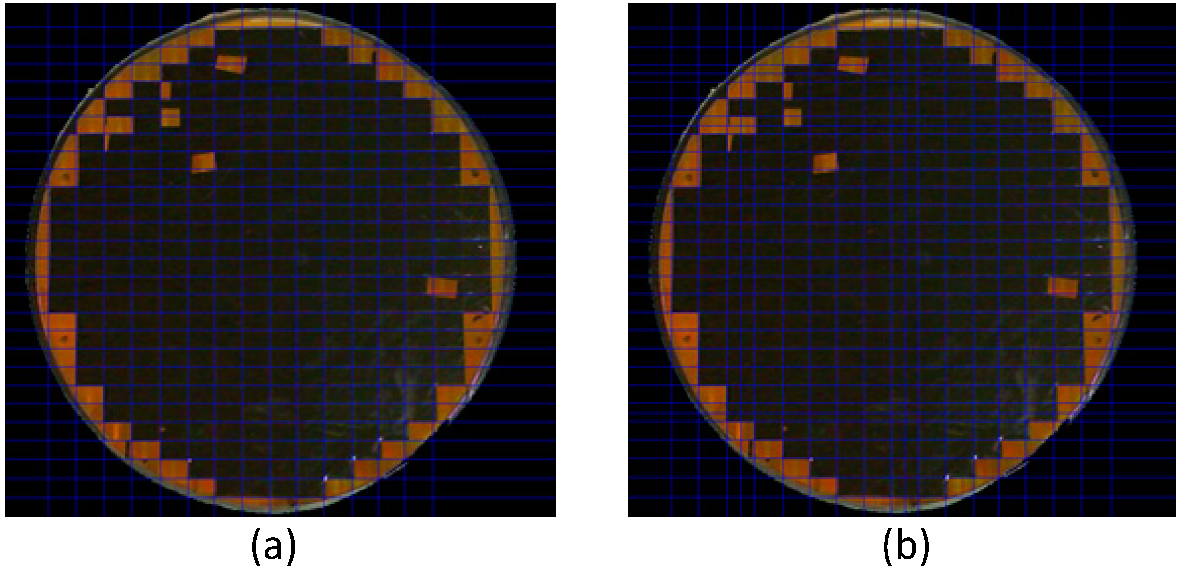
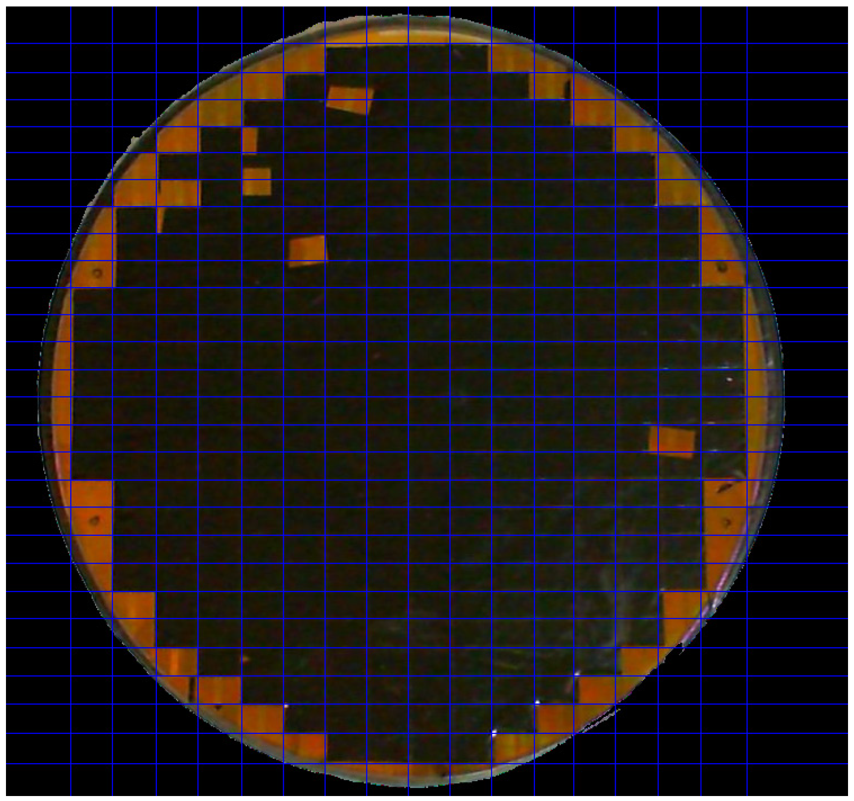
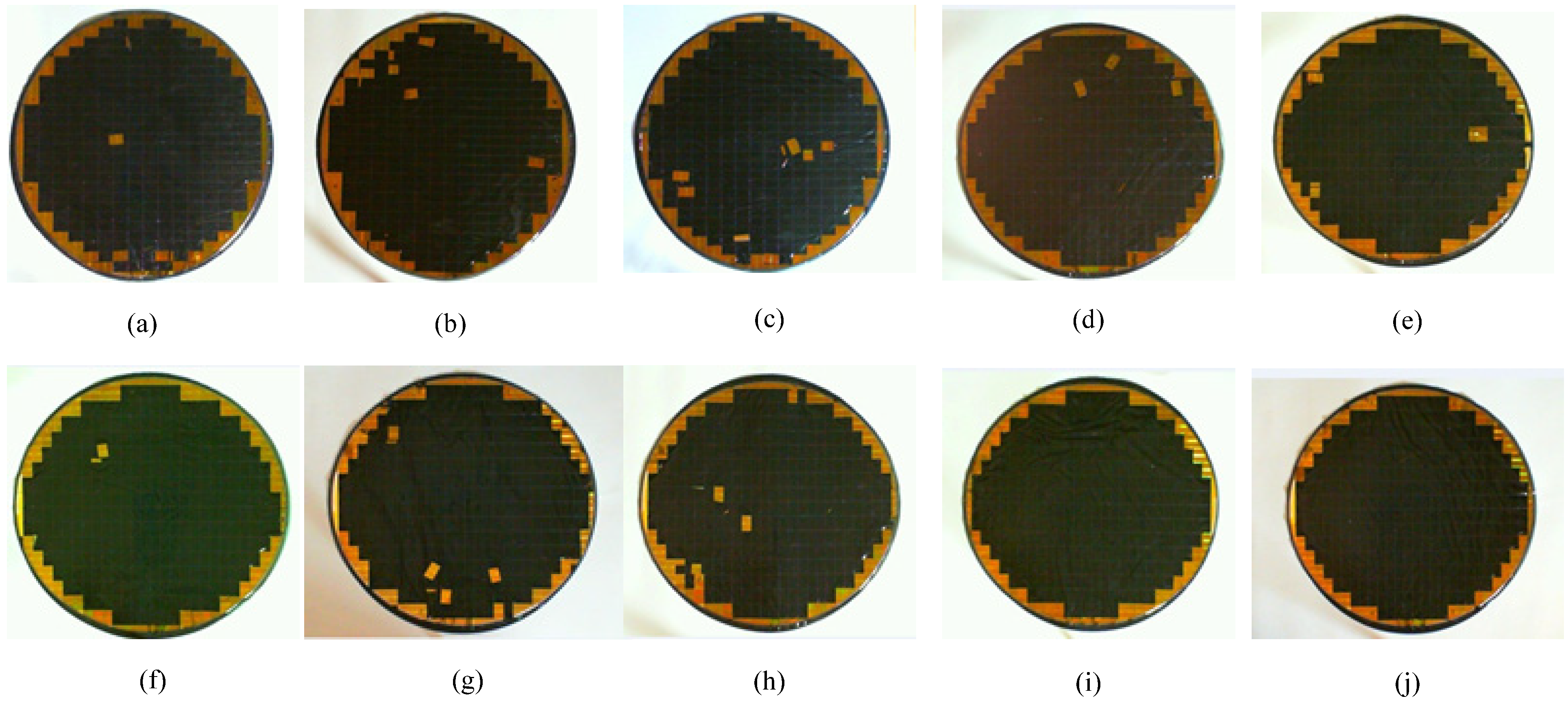
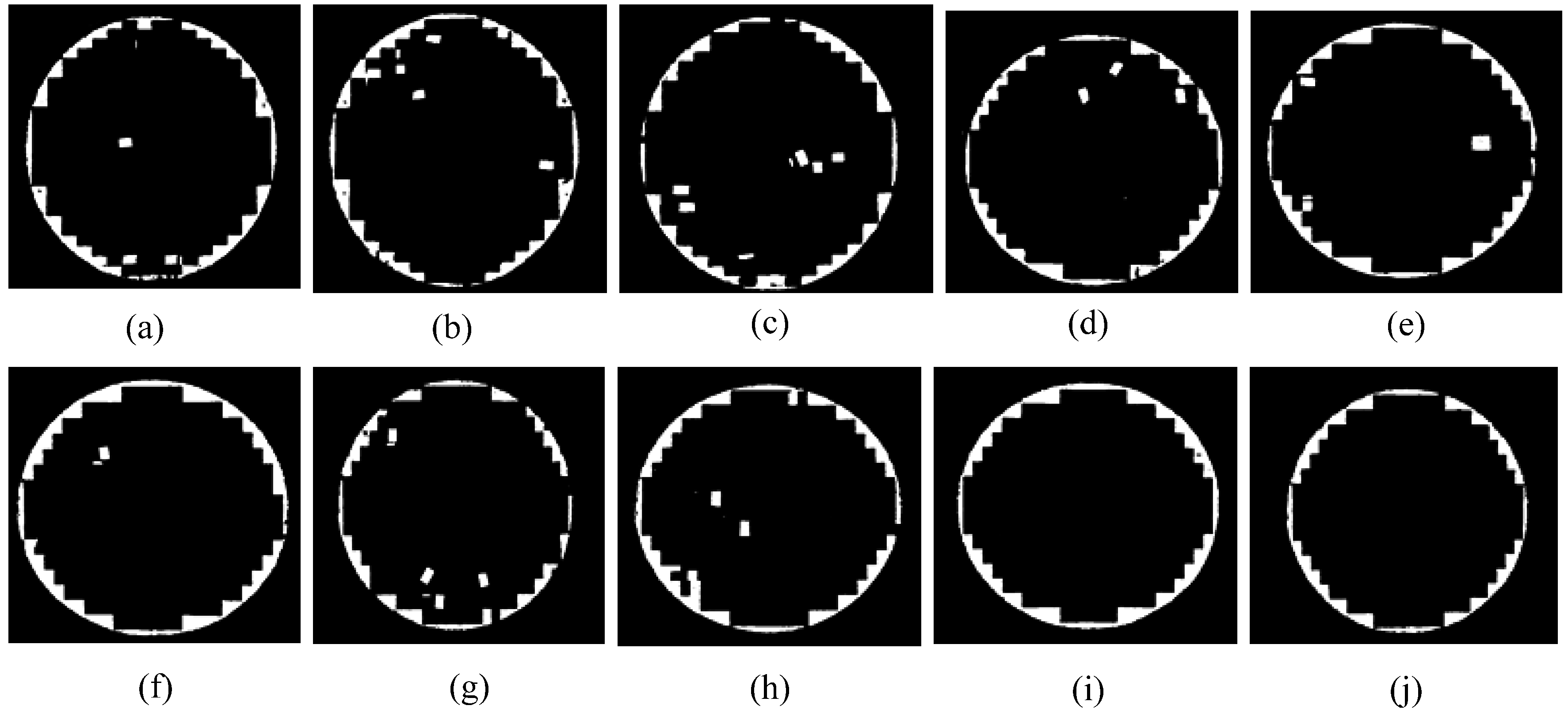
3. Experimental Results

In our experiments, a Microsoft LifeCam Cinema image sensor was used, and the computer specifications were as follows: CPU: Intel Core i5-3570K, RAM: DDR3 1600MHz 4G. The programming was implemented using Visual Studio 2008. Figure 20 shows the photographic environment. Two illumination sources were used in the experimental set up to reduce reflection effects in the captured images. According to the empirical tests in our experiments, the various threshold values in the proposed method are given as follows: both Tw and Tcb are automatically determined by using the Otsu method, Tc = 185, T = 25, Tn1 = 800, Tn2 = 700, and Ts1 = 450. The accuracy for evaluating the proposed method is defined in two aspects, the recall and precision rates, which are expressed as
Precision rate =   Number of correctly deteced dies Total number of detected dies
Recall rate =   Number of correctly detected dies Total number of dies
Figure 20. The experimental setup for taking the wafer images.
Machines 03 00072 g020
Figure 21a–j show ten samples of the all test wafer images in our experiments. Both normal and abnormal cases of the resident dies can be found in these images. Figure 22a–j show the corresponding detection results of the die regions. Figure 23a–j show the results of the detected die areas in the normal cases, while Figure 24a–j show the results of the detected dies area in the abnormal cases. Some tiny parts of the die, as shown in Figure 22b,c,f,g, can be discarded to prevent the inclusion of the number in the abnormal cases.
Figure 21. The ten test wafer images numbered from (a) to (j).
Machines 03 00072 g021
Figure 22. The results of the die region detection corresponding to the images shown in Figure 21a–j.
Machines 03 00072 g022
Figure 23. The packaged regions in the normal cases corresponding to the images shown in Figure 22a–j.
Machines 03 00072 g023
Figure 24. The results of the die regions in the abnormal cases corresponding to the images shown in Figure 22a–j.
Machines 03 00072 g024
There are 41 wafers images in total. The die numbers are divided into three situations: normal, abnormal, and packaged. As shown in this table, most of the dies in the abnormal cases can be correctly detected. Table 1 summarizes the determined numbers in the normal, abnormal, and actual packaged cases. The recall and precision rates are provided as well. In this table, the precision and the recall rates are (P/G) × 100% and 100%, respectively, when the detected number P is greater than the ground truth number G. On the contrary, the precision and the recall rates are 100% and (P/G) × 100%, respectively, when the detected number P is less than the ground truth number G. If the two numbers are equal (P = G), then both the precision and the recall rates are 100%. The recall and precision rates in the experimental results of the 41 test images achieve 99.82% and 99.84%, respectively. The computation time for each test image is around 0.7 s in average.
Table 1. The recall and precision results in the experiments.
Wafer ImageNormal (N)Abnormal (S)Packaged (P)Ground Truth (G)Precision RateRecall Rate
1315331231199.68%100.00%
2315331231199.68%100.00%
3315531030999.68%100.00%
43101031030999.68%100.00%
53231331030999.68%100.00%
63146308309100.00%99.68%
73133310310100.00%100.00%
83144310310100.00%100.00%
93184314314100.00%100.00%
103217314314100.00%100.00%
113261131531499.68%100.00%
1232611315315100.00%100.00%
133121311311100.00%100.00%
143231031331199.36%100.00%
153241231231199.68%100.00%
16315331231199.68%100.00%
173121311311100.00%100.00%
18313131231199.68%100.00%
19319731231199.68%100.00%
203216315316100.00%99.68%
213205315316100.00%99.68%
223202318318100.00%100.00%
233214317318100.00%99.69%
243121311311100.00%100.00%
25319731231199.68%100.00%
26313131231199.68%100.00%
273178309311100.00%99.36%
283177310311100.00%99.68%
293024298311100.00%95.82%
303176311312100.00%99.68%
313130313313100.00%100.00%
323152313313100.00%100.00%
333152313313100.00%100.00%
34316331431399.68%100.00%
35322731531399.37%100.00%
363182316316100.00%100.00%
373259316316100.00%100.00%
383301131931699.06%100.00%
39320331731699.68%100.00%
40319231731599.37%100.00%
413161315315100.00%100.00%

4. Conclusions

This paper presents a machine-vision-based method to automatically determine the number of successfully packaged dies in a wafer image. The most significant contribution of the proposed method is that it can handle all the cases of the residual dies, including those in the wafer boundary, broken dies, fractured dies and dropped dies in the wafer. The precision and recall rates achieved were 99.82% and 99.84%, respectively, in the 41 test wafer images.
Figure 21a–j show that the brightness and position of each wafer image are slightly different. It is influenced by the ambient light and non-fixed photographic environment. In the future work, we will improve the image capture environment such that the number of system parameters can be reduced to make the system simpler. In addition, more test images will be collected to make the proposed method more robust in the various abnormal cases.

Acknowledgments

This research is partially supported by the Ministry of Science and Technology (MOST), Taiwan under contract numbers MOST 103-2221-E-224-019 and MOST 103-2221-E-224-035 MY2. The authors thank for the reviewers’ valuable comments and the English revision made by Resta S. Cheng.

Author Contributions

Hsuan-Ting Chang has been responsible for the whole system modeling and the evaluation of the experimental results. Ren-Jie Pan and Hsaio-Wei Peng have been responsible for the experimental setup and the system implementation with Matlab coding.

Conflicts of Interest

The authors declare no conflict of interest.

References

  1. Driels, M.R.; Pathre, U.S. Vision-based automatic theodolite for robot calibration. IEEE Trans. Robot. Autom. 1991, 7, 351–360. [Google Scholar] [CrossRef]
  2. Madhvanath, S.; Govindaraju, V. The role of holistic paradigms in handwritten word recognition. IEEE Trans. Pattern Anal. Mach. Intell. 2001, 23, 149–164. [Google Scholar] [CrossRef]
  3. Kumar, A.; Yingbo, Z. Human Identification Using Finger Images. IEEE Trans. Image Process. 2012, 21, 2228–2244. [Google Scholar] [CrossRef] [PubMed]
  4. Lin, Y.S.; Lee, T.C.; Chang, H.T.; Peng, S.J.; Huang, J.W.; Wang, H.P.; Hung, C.W. A computer-aided method for automatic localization and thickness measurement of peritoneum in ultrasound images. In Proceedings of the Annual International Conference of the IEEE Engineering in Medicine and Biology Society, MA, USA, 30 August–3 September 2011; pp. 8005–8008.
  5. Gao, Y.S.; Leung, M.K.H. Face recognition using line edge map. IEEE Trans. Pattern Anal. Mach. Intell. 2002, 24, 764–779. [Google Scholar] [CrossRef]
  6. Hackenberg, G.; McCall, R.; Broll, W. Lightweight palm and finger tracking for real-time 3D gesture control. In Proceedings of the IEEE Virtual Reality Conference (VR), Singapore, Singapore, 19–23 March 2011; pp. 19–26.
  7. Zeng, Z.; Dai, S.; Mu, P.A. Wafer defects detecting and classifying system based on machine vision. In Proceedings of the International Conference on Electronic Measurement and Instruments, Xi’an, China, 16–18 August 2007; pp. 4-520–4-523.
  8. Wu, H.H.P.; Yang, J.G.; Hsu, M.M.; Wu, C.J. Automatic measurement and grading of LED dies on wafer by machine vision. In Proceedings of the IEEE International Conference on Mechatronics, Kumamoto, Japan, 8–10 May 2007; pp. 1–6.
  9. Wang, G.; Li, D.; Wu, L.; Deng, Y.; Liu, R. Machine vision recognition of disconnection failure of IC wafer. In Proceedings of the International Conference on Electronic Packaging Technology, Shanghai, China, 26–29 August 2006; pp. 1–4.
  10. Sharma, G.; Kumar, A.; Rao, V.S.; Soon, W.H.; Kripesh, V. Solutions strategies for die shift problem in wafer level compression molding. IEEE Trans. Compon. Packag. Manuf. Technol. 2011, 1, 502–509. [Google Scholar] [CrossRef]
  11. Croft, G.D.; Lomenick, R.L.; Youngblood, D.L.; Johnston, J.M. Die-counting algorithm for yield modeling and die-per-wafer optimization. SPIE 1997, 3216, 186–196. [Google Scholar]
  12. Cunningham, J.A. The use of evaluation of yield models in integrated circuit manufacturing. IEEE Trans. Semicond. Manuf. 1990, 3, 60–71. [Google Scholar] [CrossRef]
  13. De Vries, D.K. Investigation of gross die per wafer formulas. IEEE Trans. Semicond. Manuf. 2005, 18, 136–139. [Google Scholar]
  14. Magee, M.R.; Beer, M.D.; Erck, W.R. Computation of Die-Per-Wafer Considering Production Technology and Wafer Size. United States Patent US 6,529,790, 4 March 2003. [Google Scholar]
  15. Die Per Wafer Calculator 1.00. Available online: http://mrhackerott.org/semiconductor-informatics/informatics/toolz/DPWCalculator/Input.html (accessed on 6 April 2015).
  16. Die-per-Wafer Estimator. Available online: http://www.silicon-edge.co.uk/j/index.php/resources/die-per-wafer (accessed on 6 April 2015).
  17. Mital, D.P.; Teoh, E.K. Computer based wafer inspection system. In Proceedings of the 1991 International Conference on Industrial Electronics, Control and Instrumentation, 28 October–1 November 1991; pp. 2497–2503.
  18. Su, C.T.; Yang, T.; Ke, C.M. Neural-network approach for semiconductor wafer post-sawing inspection. IEEE Trans. Semicond. Manuf. 2002, 15, 260–266. [Google Scholar] [CrossRef]
  19. Chang, H.T.; Pan, R.J. Automatic counting of packaged wafer die based on machine vision. In Proceedings of the 2012 International Conference on Information Security and Intelligent Control (ISIC 2012), Douliu, Taiwan, 14–16 August 2012; pp. 274–277.
  20. Xu, S.; Cheng, Z.; Gao, Y.; Pan, Q. Visual wafer dies counting using geometrical characteristics. IET Image Process. 2014, 8, 280–288. [Google Scholar] [CrossRef]
  21. Wafer Chip Counter—IVC12. Available online: http://www.ivtech.com.tw/ (accessed on 6 April 2015).
  22. Fischler, M.A.; Bolles, R.C. Random sample consensus: A paradigm for model fitting with applications to image analysis and automated cartography. Commun. ACM 1981, 24, 381–395. [Google Scholar] [CrossRef]
  23. De la Fraga, L.G.; Dominguez, G.M.L. Robust detection of several circles or ellipses with heuristics. In Proceedings of the IEEE Congress Evolutionary Computation, New Orleans, LA, USA, 5–8 June 2011; pp. 484–490.
  24. Otsu, N. A threshold selection method from gray-level histograms. IEEE Trans. Syst. Man Cybern. 1979, 9, 62–66. [Google Scholar] [CrossRef]
  25. Gonzalez, R.C.; Woods, R.E. Digital Image Processing, 2nd ed.; Prentice-Hall, Inc.: New Jersey, NJ, USA, 2002. [Google Scholar]
  26. Canny, J. A computational approach to edge detection. IEEE Trans. Pattern Anal. Mach. Intell. 1986, PAMI-8, 679–698. [Google Scholar] [CrossRef]
  27. Kim, Y.T. Contrast enhancement using brightness preserving bi-histogram equalization. IEEE Trans. Consum. Electron. 1997, 43, 1–8. [Google Scholar] [CrossRef]

