1. Introduction
Today, data transmission of telephone calls, video and computer data mainly relays on copper cable technology where transistors amplifies electrical signals [
1]. In the future, however, data transmission will presumably be based on optical light signals running through glass fibres. The reason for this techno-logical change is that by using pulses of light much more information can be transmitted in less time than with copper technology. However, since the primary data signals such as sound from a microphone, or data from a computer, are generated in electrical form, fast switches are necessary to transform electrical into optical signals. In order to take advantage of the broad bandwidth of glass fibres these switches have to operate on a gigahertz scale [
2]. This goal cannot be achieved in a classical way but requires the use of new materials with nonlinear optical properties. Nonlinear optical properties differ from classical linear optical effects such as reflection and refraction in that they occur at high light intensities as can be generated with a laser source. They include frequency doubling (red light can be transformed into blue light) and changes of the refractive index by applying an outer electrical field [
1,
2,
3]. While frequency doubling is used primarily for measuring and quantifying Nonlinear optics (NLO) effects the control of the refractive index can be used to modulate the intensity of light by means of an electrical field. Thus, NLO materials incorporated in an electro-optical device permit electrical and optical signals to “talk” to each other [
3]. A lot of organic nonlinear optical materials have been studied, because of their several advantages over their inorganic counterparts. These advantages include high nonlinear optical coefficients, fast response time, low dielectric constant, tailor ability of the molecules and so forth. The search for new organic nonlinear optical materials has been put on a scientific basis only after the establishment of the correlation between their nonlinearity and intramolecular charge transfer processes [
4]. The value of the second-order optical nonlinearity is directly connected with dipole moment variations occurring upon excitation of the system. Thus, one of the most important factors is the investigation of the spectroscopic properties of NLO active molecules, taking into account their material environment (solvent, polymers, sol-gel matrices). Polymers for optical signal processing applications have been attracting because of their potential use for second-harmonic generation (SHG) and for high-speed optical switching and modulation [
5]. The group of Larry Dalton, now in the University of Washington, has reported high electro-optic coefficients (up to 80 pm/V in the near IR range) in guest-host systems involving highly conjugated chromophores bearing bulky side groups to prevent the formation of centro-symmetric aggregates during material preparation. 10 Gb/s modulators have been proposed by a spin-off company of this group, Pacific Wave Industries but this product did not spread out on the optoelectronic device market [
1,
2,
3]. The main problems being the stability of chromophore polar orientation in a guest-host material. Therefore, one of the key issues in the realization of polymer-based optoelectronic devices is to ensure a good temporal stability of the polymer’s ordering, so as to meet the requirements for further applications in optical communication systems (i.e., long-term stability at temperatures as high as 85 °C). For second-order NLO polymers utilizing an external field to achieve orientation of chromophores such poling-induced order is thermodynamically unstable. To prevent the relaxation of the aligned chromophores various approaches have been proposed. Larry Dalton’s group is currently working of dendritic polymerization schemes so as to stabilize the polar orientation and to prevent aggregation. A second promising approach is to use high glass transition temperature (T
g) polymers such as polyimides, a category of polymers already well-known in microelectronics, that possess exceptional thermal, mechanical, optical and dielectric properties. The first use of polyimides as NLO materials was in guest-host systems, that is, mixtures of low-molecular weight NLO chromophore molecules with high-molecular weight polyimides [
4,
5,
6,
7,
8]. However, these systems have shown problems such as low loading density of chromophores and rapid relaxation of poling-induced order. To overcome these problems, functionalized polyimides with covalently bonded chromophores have been studied. But the poor solubility of many polyimides in common solvents makes it difficult to obtain good optical quality films. High intramolecular charge-transfer molecules such as Disperse Red-1 and its derivatives were mainly used as chromophore side groups but using more classical, low T
g polymer backbones such as polymethacrylates or polycarbonates. Reasonable values of second-order nonlinearity were obtained (typical electro-optic coefficient of DR1-functionalized polymers amounts up to 20 pm/V at 1.3 µm) [
5]. For polyimides with covalently bonded chromophore groups the situation is in fact much more difficult than in lower T
g polymers such as PMMA, polycarbonate and related matrices. In the case of polyimides the electronic and therefore NLO properties of the monomeric subunit containing the active NLO chromophore may be affected by the highly conjugated character of the polymer backbone [
6]. In the last few years several researchers have been involved in recent technology developments, for new biomedical applications, using near-zero-index materials, metamaterials, metasurfaces, nanoparticles, graphene and so forth.
The advances in the field of electromagnetic metamaterials and plasmonic optics have enabled control over the flow of light in engineered nanomaterials, to realize materials with effective refractive which indices that range all the way from positive to negative values [
9].
Metallic nanoparticles exhibit unusual optical properties deriving from the strong local electromagnetic field in the neighbourhood of the structure under the Localized Surface Plasmon Resonance (LSPR) excitation [
10].
These electromagnetic properties make metallic nanoparticles suitable for several application fields: biochemical sensing and detection, protein analysis, food quality analysis and therapeutic applications as photo thermal destruction of cancerous cells [
10].
In the recent review, the authors introduce advances and potential applications of Electromagnetic metamaterials (MMs) and metasurfaces (MSs) for various sensors. Mainly classify sensor applications into two major objects of MMs and MSs sensing: RI sensing with optical response and sensing properties of light itself [
11].
The existing literature has mainly focused on the experimental evaluation of the nanoparticle electromagnetic characteristics but it is almost silent on the development of proper analytical models and design methods describing their resonant behaviour, with few exceptions [
12]. In particular, the authors of the paper [
12] present a new design method for ellipsoidal nanoparticles with the desired electromagnetic properties, in order to satisfy specific requirements.
We can use this theoretical study showing that by designing and manipulating spatially inhomogeneous, nonuniform conductivity patterns across a flake of graphene, as a one-atom-thick platform for infrared metamaterials and transformation optical devices [
13].
In a previous study we presented an e-Health Internet of Things solutions for biomedical applications that can solve the growing demand for health care systems with limited environmental resources using the energy autonomy of the medical technologies based on high efficiency organic solar cells [
14].
3. Results
The
Figure 2,
Figure 3 and
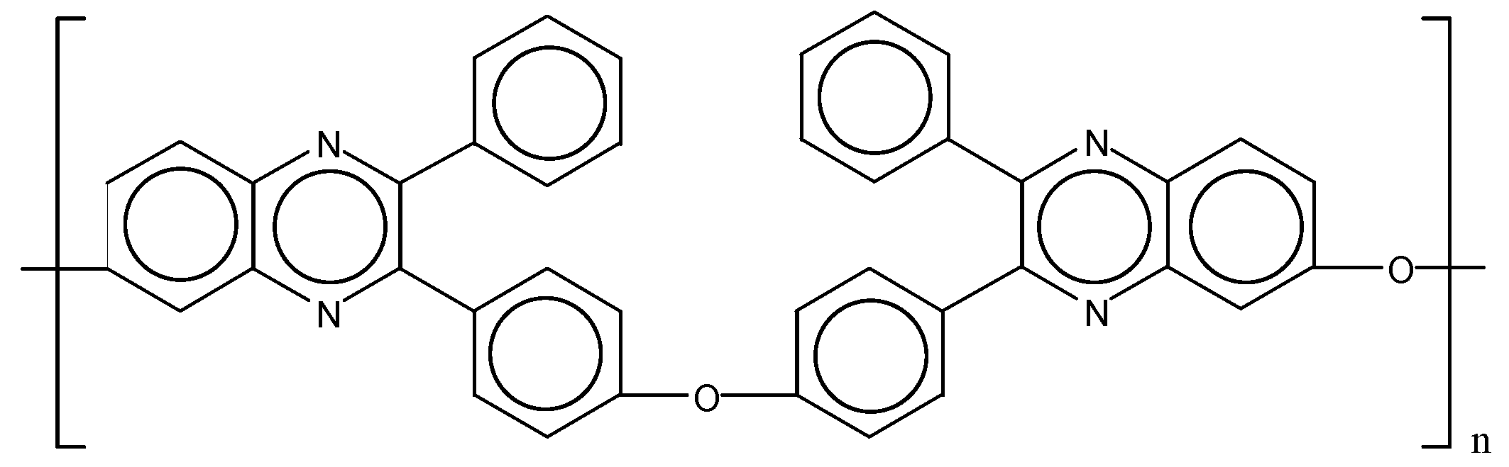
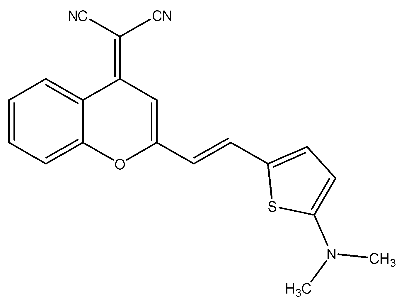
Figure 4 show the chemical structure of three new chromophores investigated so far in PPQ-eth guest-host systems.
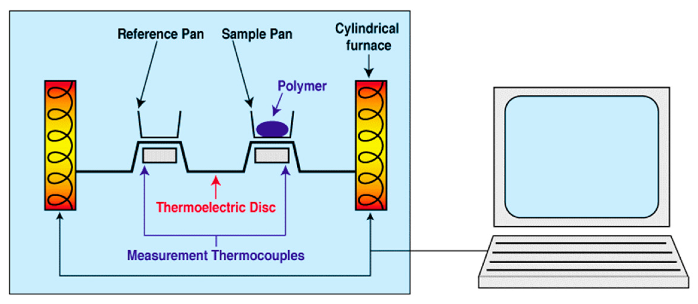
The thermal properties of the matrix material PPQ-eth, of the chromophor CH01 and of the host-guest systems have been investigated by means of thermogravimetry (TGA), differential scanning calorimetry (DSC,
Figure 5), DSC curves measured (
Figure 6) and Thermally Stimulated Depolarization Currents (TSDC,
Figure 7). While TGA provides the temperature of the onset of thermal decomposition (T
d) and the temperature where 5% of weight loss occur (T
d5) both measured with constant heating rate of 20 K/min. The results are collected in
Table 1.
DSC technique was used to determine the glass transition temperature (T
g) of the polymer, also measured with constant heating rate of 5 K/min. The DSC setup is show in
Figure 5.
In addition to the pure polymer PPQ-eth also mixtures of the polymer with three different chromophores (CH01 to CH03, introduced below) have been analysed by TSDC measurement [
21].
The introduction of chromophores leads to a clear decrease of the glass transition temperature [
22]. The TSDC can provide the energy of molecular motion activation, such as the dipolar rotation of the main chain and this can be used to determine the transition temperature to the glass phase. In a normal TSDC experiment a sample is polarized at high temperature, which means an electric field of the order of 10
5 V/cm [
22,
23,
24,
25] Then the sample is cooled down to the liquid nitrogen temperature or below. During cooling under the effect of the applied field, the polymer dipoles retain their orientation. At low temperatures, the current is blocked, the sample being shorted to a sensible picoamperometer and after a few minutes at low temperature, when the electric bearers do not show up, the sample is heated in a controlled manner and the short-circuit current is measured according to the temperature. The purpose of a TSDC experiment is to deduce specific load release from the obtained thermograms of kinetic parameters. Theoretical the current discharge treatment arises from a supposed polarized sample that does not present a current coming from the electron trap and hole trap, dipolar polarization in this case is considered spatial and independent. Unfortunately, spatial load and dipolar polarization coexist in real samples and with a single TSDC experiment, it is impossible to distinguish between the peaks due to the decaying of charged loads and peaks having a dipole origin. However, it can be expected that the energy distribution of the localized loads is large and almost homogeneous throughout the sample. In any case, dipole peaks are readily recognizable when an experiment is carried out by clearly destroying the current increase due to the decapitation effect. Assuming a Debye model describing the Debye equation, the increase in polarization during the high temperature formation period
P can be described by an exponential time function (2) which is the solution of Equation (1):
In Equation (2), an ideal rotation friction pattern is assumed; C is the constant of polarization at equilibrium and τ is the dipole relaxation time.
During a TSDC experiment, dipoles are disoriented at a rate that can be described by the Debye model. After removing the external field, two competitive effects are responsible for the emergence of a maximum TSDC. On the one hand, the dipoles are oriented but fictions and on the other hand, the actions of thermal movement with the rise of the random dipole temperature. Then, considering a relaxation time of polarization identical to the relaxation time of depolarization, Equation (1) describes the decrease of depolarization:
The density of the current generated during the drop is described by Equation (4).
The current density
J(
t) in Equation (4) is a function of time. However, when a TSDC experiment is perfected, then the time-temperature dependence is well known. Assuming a constant
β rate, which is used for a TSL experiment, according to Equation (1), it is possible to write polarization as (5).
Finally, by incorporating Equation (5) we obtain an expression (6) describing a TSDC peak.
In Equation (6) the variance of τ as a function of temperature is given by the Equation (7), equivalent to (6), which describes the probability of an electron to be released from a trap.
In Equations (6) and (7) τ0 is the relaxation time at an infinite temperature and corresponds to the inverse of the natural relaxation frequency αr. It gives the activation energy to relax the dipoles.
Equation (6) describes a simple maximum of relaxation current for a first-order thermoluminescent peak. The first integral dominates the initial part of the peak. At high temperature, the exponential side dominates and the signal decreases.
The existence of relaxation time distributions can be explained in polymers by several mechanisms, such as dipol-dipol interactions or internal anisotropy. In addition, the simple approach, for example the combination of singular peaks, gives excellent results corresponding to a real TSDC thermogram.
The simple Equation (5) describes a TSDC peak at a distance from the transition region to the vitrified phase. In this particular case there are different phenomena related to changes in the free volume. In literature, there is an approach to this problem, made by Schrader [
22,
23,
24,
25]. In its analysis, an unexponential decrease in kinetic time dependence is proposed. Time dependence is the result of combining cooling in the transition region to the glass phase, so polarization is frozen and subsequent heating when the current density variation is recorded. Schrader’s approach allows a qualitative description of the TSDC evolution as well as the record of the high temperature of the thermograms.
A suitable model to facilitate the interpretation of the results comes from the thermal technique, which establishes a theoretical correlation between the DES and TSDC measurements. The two techniques are fundamentally different: while TSDC is a non-isothermal technique, where time and temperature vary according to a well-known relationship, DES is an isothermal technique.
In a DES experiment on the sample, a sinusoidal electrical signal is applied. Dipoles try to follow the frequency but because they cannot respond instantly to voltaic changes, there are phase shifts between the applied signal and the system response, changes that are recorded. The signal coming from dielectric material can be described by a complex
ε dielectric function in Equation (8).
The real and imaginary parts of the above expression depend on the temperature and frequencies applied by Equations (9) and (10).
The quantity Δ
ε does not describe the relaxation of the forces through the following Equation (11).
In the above equations we have: ε0 low dielectric constant—static limit, while ε∞ is the high frequency dielectric constant—called optical limit and ω is the applied angular frequency.
We can impose the equivalence (12) between the maximum relaxation peak and the maximum peak of the TSDC current.
The main condition for the imaginary part of the dielectric complex constant can be found by differentiating (10) taking into account the applied frequency.
The condition for the maximum equivalence is given by Equation (15).
Based on Equation (15) it is possible to write the maximum for the dipole relaxation time
τmax, i.e., the Equation (16), which is used for non-isothermal dielectric measurements at an
ω angular frequency constant:
Solving the Equations (16) we find the maximum temperature for the dielectric peak (20).
Using the conditions (15) and (16) we can write using
:
Then the maximum temperature expected in the case of a dielectric maximum is given by the following Equation (20)
In Equation (20), ω indicates the applied angular frequency, while ω0 is the frequency of the dielectric peak in the investigation. Equation (20) allows the determination of the temperature range around Tm to verify that a maximum of a TSDC spectrum is of a dipole type. The ω value indicates the frequency used to measure the DES peak and can be approximated to the value of 1 × 10⁴ Hz, a mean value of the useful range of the standard devices used in the electrical measurements.
The quantity ω0 indicates the natural frequency factor of the TSDC and ε’’ peaks. This value can easily be calculated by numerical analysis of the TSDC curve. The thermal stimulation technique has a high resolution for dielectric spectroscopy.
For this reason, the absence of a DES peak in the equivalent temperature does not mean that the TSDC peak does not have a dipole origin. In addition, analysis is needed to verify some assumptions. A new problem arises from the fact that DES peaks measured at frequencies above 0.1 Hz are expected to occur at elevated temperatures like the TSDC peaks. Correct TSDC peak resolution is often equivalent to DES at high temperature, which is a temperature beyond which the sample can be destroyed. All of this information is inaccessible to DES measurements and it is impossible to verify the hypothesis of the dipolar peak. On the other hand, the main condition for a TSDC peak can be derived as follows. Considering the Equation (4) and derivating we can write:
From the Equation (21) in accordance with van Turnhout’s theory [
22,
23,
24,
25], it is possible to check whether the maximum current occurs at:
or the equivalent:
Based on Equations (22) and (23) it is demonstrated that the main condition for a Debye peak can be written using the following equation:
By comparing the Equations (20) and (23) we can find a relationship between the heating rate
β of a TSDC experiment and an “equivalent frequency” in which a non-isothermal DES experiment is performed to find the maximum at a higher value of
, at the same temperature as in DES:
This equation establishes the “equivalent frequency” of the TSDC experiment, which depends on the heating rate and also on the material parameters, such as the average activation energy of the relaxation process.
PPQ-eth is well soluble in chloroform, 1,1,2,2-tetrachloroethane and N-methyl-pyrrolidone and the same holds for the three chromophores. PPQ-eth and PPQ-eth-dye-systems form homogeneous and smooth LB films and spin coating from solutions of 1,1,2,2-tetrachloroethane [
20,
26].
In
Table 2 we show the thickness per monolayer for N-type multilayers of PPQ-eth/dye (CH01) deposited on different kinds of substrates determined by multiple angle ellipsometry. The monolayer was formed by spreading 50–150 µL of the solution.
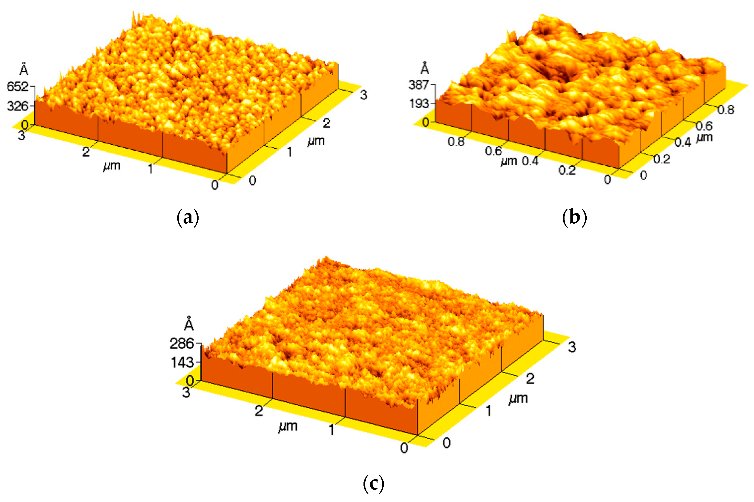
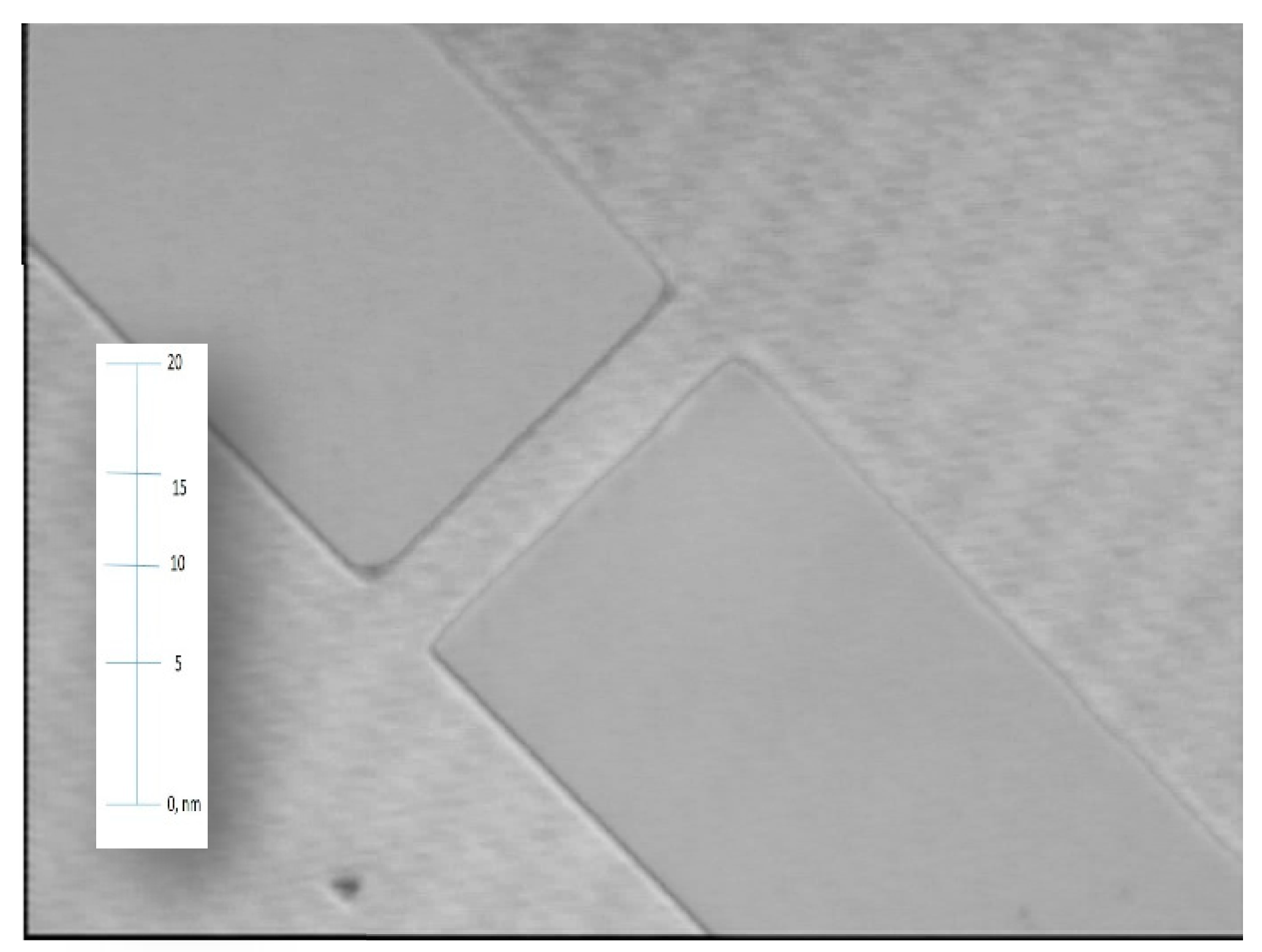
The surface morphology of the films was obtained using an atomic force microscope (Autoprobe VP 2 Park Scientific Instruments), operating in noncontact mode in air at room temperature.
The thickness of the investigated thin films was measured using a Dektak Profilometer (DEKTAK 3 from Veeco Instruments) device, which has the capability of measuring the step height down to a few nm. Scan area of 3 μm was chosen and the surface root mean square roughness R
rms was measured on all the samples at a constant tip force as can be seen in the AFM images (
Figure 8 and
Figure 9). R
ms roughness was low as 2 nm [
26].
Promising is the low value of rms roughness, which indicates that high quality optical wave-guides might be prepared from those materials.
The absorption properties of the host material are characterised by a main peak at 373 nm as can be seen in
Figure 10.
In the visible range only the chromophores contribute to the absorption.
First SHG experiments on poled guest host systems (for beginning we measure only PPQ-eth-CH01) lead to encouraging results as can be deduced from the results of SHG experiments plotted in
Figure 11.
There the SHG intensities of the bare substrate (glass coated with indium tin oxide–ITO), of the substrate with an unpoled polymer/chromophore layer and a poled polymer film are shown in dependence on the rotation angle of the sample (angle of incidence). A strong SHG signal can be seen after corona poling. More detailed investigations in dependence on layer preparation and poling conditions are on the way.
The guest-host system CH01/PPQ-eth shows a promising combination of high nonlinearity and thermal stability. Clearly the strongly enhanced SHG signal after poling can be seen. A glass transition temperature around 230 degree provides long life-time of the “frozen” state of nonlinear moiety and extends demesne of optical devices based on such dye-polymer system. In order to better understand the intensity obtained in SHG experiment, we have done also the XRD measurements on two spin coated guest-host system CH01/PPQ-eth films on silicon (
Figure 12). There is a strong peak at 28.4 degrees which comes definitely from the silicon single crystal substrate. It is the 111 peak, which is obviously the cutting direction of your wafer. The missing second reflections can be explained simple by the fact that the wafer is cut with the 111 plane parallel to the surface substrate and with the used method only planes parallel to the substrate appears. Another effect which does not come from the polymer layers is the increasing intensity at low angles, below 10 degrees 2THETA. 2THETA is always the scattering angle it is the total angle between the primary beam and the scattered beam. This arises due to scattering of X-rays on air and Fresnelsche reflectivity of X-rays from the surface. The signal from polymer is a broad halo with an onset at 15 degrees, a maximum at around 22 degrees and the halo ends at 38 degrees. This broad halo arises due to the amorphous structure of polymer. More than less in all amorphous polymers such a halo arises at the same position. From the height of the diffraction signal, we would say that the film it was relatively thick, probably in the micrometre range. The samples were measured with CuK_alpha radiation in Bragg-Brentano geometry using a secondary graphite monochromator. Equipment was a SIEMENS D501 powder diffractometer operation in THETA/2THETA mode (specular mode).
4. Applications
In order to improve the performance of integrated photonic devices we developed a first silicon slot waveguides covered with CH01/PPQ-eth. In parallel, we try to pull optic fibres into these materials and use our products in fibre optic sensors. First of all, we described the fabrications steps and investigate the surface properties. It describes typical pattern fabrication steps and the limits of current fabrication techniques. This is followed by the theory and practice of slot waveguide based electro-optical modulators. This application can be used in ring resonators based on a slot waveguides. A great number of researches showed that this concept allows low energy consumption by reducing the capacitance length and using advanced nonlinear optical polymers. The slot waveguide is embedded in an organic nonlinear optical material in order to achieve record-low voltage-length products. In the field of optical sensors, it is showed that slot waveguides enable remarkable waveguide sensitivity for both refractive index sensing and surface sensing.
Film composition can be controlled by judicious choice of the monomer added at each step. This enables the inclusion of diverse functionality into the polymer film. When multifunctional monomers react with the functionalized surfaces, crosslinks can be formed. These crosslinks are unique because they form only at the surface and not in solution (
Figure 13). At the surface, crosslinking aids to increase the durability of the film but reduces the number of active chains for film growth.
In this case, film growth is continued because of the hyperbranched nature of the polymer. In solution surrounding the surface, the monomers cannot react with each other and crosslinking is negligible.
In addition to characterization by XPS, the growth of hyperbranched polymer films was studied by micro-patterning techniques. In patterning, initiator molecules are spatially defined on a surface. This enables polymerization to occur only at specific regions and yields adjacent control regions on the surface.
In order to transfer initiator molecules to surfaces, a CH01/PPQ-eth) stamp was prepared. The CH01/PPQ-eth stamp was prepared by etching a pattern onto silicon, using photolithography and reactive ion etching, RIE, techniques, pouring prepolymer onto the etched silicon, curing the polymer and detaching the polymer from the mould [
18,
19,
20]. The patterning is illustrated in
Figure 14. This indicated that during the Heck reaction, monomers reacted with the chemisorbed initiator molecules patterned on the surface and did not physisorb onto unpatterned regions (
Figure 15).
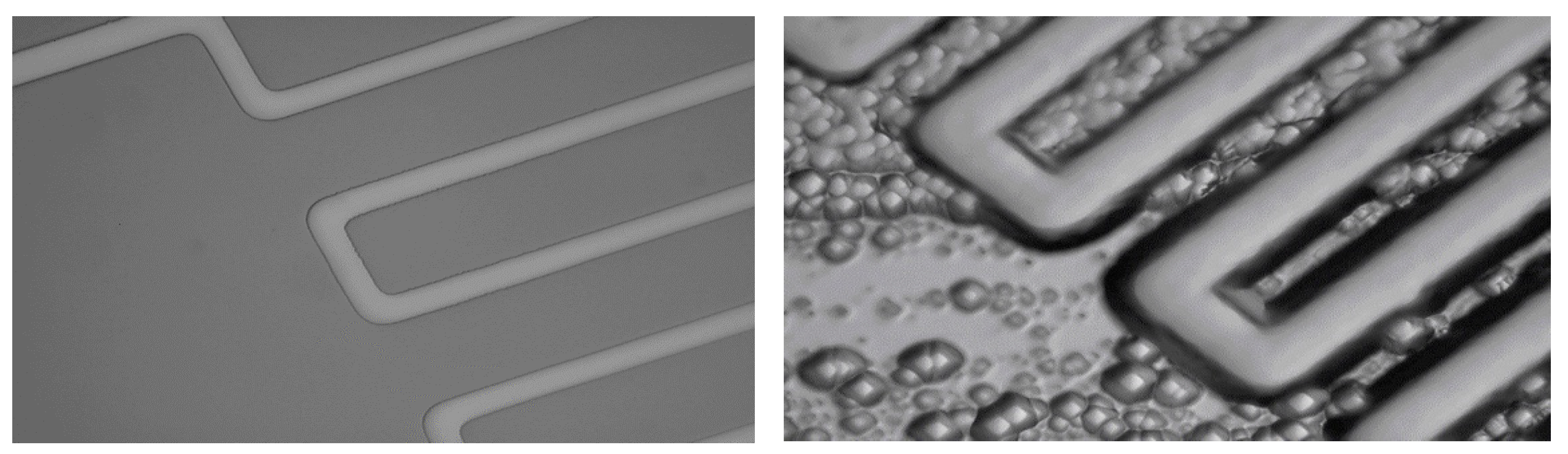
The patterned lines of 10 were measured to be 20 µm wide separated by 10 µm. These dimensions can be compared to the original photolithography mask having lines 10 µm wide separated by 30 µm. The increase in the width of the lines from the mask to the pattern can be explained by anisotropoic etching of the silicon mould prior to the formation of CH01/PPQ-eth stamps (
Figure 16).
In order to determine the upper limit of film thickness as well as the degree of coverage in the patterned region, an atomic force microscopy (AFM) image was taken across a scratch in the functionalized region of the pattern (
Figure 17). The AFM image showed that the scratch was 10 µm wide surrounded by many individual features with an average height of 30 µm. The features were attributed to polymer growth from the surface, yielding an upper limit of film thickness at 30 µm, assuming that the base of the scratch was at the same level as the base of the polymer. The degree of coverage of the patterned area was observed to be incomplete. This could be due to inefficient transfer efficiency of initiator molecules to the surface during the stamping process. CH01/PPQ-eth stamps are known to transfer molecules with long alkane chains efficiently but are less effective in the transfer of non-alkane chain moieties.
Once DVP polymerization is controlled, unique monomers can be reached at different distances from the surface using the stepwise approach.
Also, fibre sensors and optical wave guides from CH01/PPQ-eth are guided devices based on optical principles and laws to monitor physical phenomena, chemical, biomedical and so forth. (
Figure 18). Thus, the variation of physical, chemical, biological, medical and so forth parameters. is transformed with an optical modulator in electrical quantities (voltages, currents) which are then detected and measured. Incident light coming from an optical source (which is generally a laser) is transmitted using an optical fibre in a device (modulator) in which it is modulated by a physical, chemical or biological phenomenon.
Modulated (emerging) light is also transmitted back through an optical fibre to a receiver, detected and demodulated. The receiver can be built in such a way that there is a one-to-one correlation between the phenomenon studied and the demodulated signal. A sensor is a device that takes values of a physical size (temperature, pressure, etc.) and converts them into electrical quantities (currents or voltages) directly usable through a data control or acquisition system. A transducer is a device that takes the value of a physical size and transforms it into electrical magnitude.
The difference between a sensor and a transducer lies in the presence of that part of the system that outputs a normalized electrical signal directly proportional to the measured magnitude and as few errors as possible. Optical fibre sensors have been the subject of great research efforts in recent years. Sensors of this type offer many advantages over conventional detection techniques, including a high sensitivity to measuring physical parameters (such as temperature, pressure, vibrations, etc.).
Optical fibre sensors are built from dielectric materials, so they can be used at high voltage, large electrical and magnetic fields, high temperature and so forth. In recent years, several types of fibre optic sensors have been developed. Basic fibre sensor components and waveguides having a generally simple construction allow the cost reduction of manufacturing them. Fibre-optic sensors can be classified into several categories according to various criteria. Based on current technology, optical fibre sensors can be configured to operate in distributed mode in which the parameter of interest to be measured is monitored at several points along the fibre optic.
There are two types of distributed sensor systems. Intrinsically distributed sensors, in which the measured parameter can be evaluated at any point of the optical fibre, the spatial resolution being generally determined by optoelectronic constraints. In this case, the fibre acts as a sensor along its entire length. The operation of this type of sensors is based on Rayleigh, Raman and Brillouin scattering.
Quasi-distributed sensors, in which the measurement parameter (field) is determined, in a certain number of predefined regions (sensor). In this case, the fibre acts as a sensor only on certain portions and their operation is generally based on retrospective phenomena. Also, if the fibre acts as a sensor on a large portion, a wide-range transmitting device with the transmitted type is obtained. Sensor fibre can also be placed at one end, producing reflective sensors and expanded integration step respectively (
Figure 19). Much of the devices used to measure the various parameters: temperature, pressure, displacement, magnetic field and chemical agents are part of the intensity sensors category. Their operation is based on: differential absorption (colorimetry), emission (black body), fluorescence/luminescence, standard cavities.
Fibre-optic sensors can also be classified by the following scheme. Based on the modulation and demodulation process, a sensor may be referred to as a sensor of intensity, a phase sensor, a frequency sensor, or a polarization sensor. Since phase or frequency detection in optics requires interferometric techniques, this type of sensor may be called interferometric sensor and from the point of view of detection, there is an interferometric technique involving heterodyne detection/coherent and incoherent detection respectively. Intensity sensors are characterized by incoherent detection. The advantage of modulated intensifier sensors is simple and compatible with multimode fibre technology, while coherent detection interferometric sensors are more complex but offer better sensitivity and resolution. The optical sensors with reflection are included in the modulated intensifier sensors category.
Interferometric sensors have the advantage that the measurement is related to an intrinsic property such as speed, wavelength or frequency. These sensors are generally characterized by a more complex construction than intensity sensors. To make measurements with this type of sensor, a high precision alignment of the optical components that make up the interferometer is required. In a single-fibre, the coherent properties of the propagated beam are maintained, so it is possible to construct an interferometer from a single monomodal optical fibre. This allows for flexible interconnections in the sensor detection system and eliminates problems related to the geometric instability of conventional interferometers.
The light emitted by the optical source (laser) is coupled to a fibre, then the light beam is injected into the interferometric sensor and finally it gets through another optical fibre to an optical detector, usually a photodiode, to process the signal). Taking into account their applications, fibre-optic sensors can be classified into: Physical sensors (for measuring temperature, pressure, etc.); Chemical sensors (e.g., for pH measurement, gas analysis, spectrometric studies); Bio-medical sensors (e.g., biomedical spectroscopic sensors, sensors that simultaneously measure pH, CO2, O2, sensors that monitor blood flow). Both sensors, of intensity and interferometric type, can be considered as part of any of the previous applications.
The sensors can also be classified into intrinsic and extrinsic sensors. This classification is considered to be the most general. A sensor is considered to be intrinsic if a fibre optic transducer is used, the relevant part serving as a sensor, usually not distinguishable from the rest of the optical fibre. In contrast, an extrinsic sensor (uses an optical fibre to lead the light to the detector or device and another fibre, identical or not with the first, is used to drive the processed light to a photodetector system.
5. Conclusions
Chemisorbed organic thin films of hyperbranched PPQ polymers were prepared in a controlled, stepwise fashion from various substrates. The novel high-temperature resistant polymers with nonlinear optical properties have been synthesized, characterized and tested for use in electro-optical components with high bit rate optical signal processing systems and for dynamic holography. These films were grown using optimized Heck reaction conditions and were characterized by measurement of second-order nonlinear susceptibility by second harmonic generation, UV-VIS spectroscopy, XRD measurement, dielectric relaxation, glass transition temperature and molecular weight distribution before and after artificial ageing. Also we have done AFM, SEM investigations and profilometry measurements for stamp patterning layers. Although surface coverage was not continuous in regions where the polymer pattern touched the surface, the contrast between functionalized and unfunctionalized regions was distinct. It is predicted that as the branched polymer grows, the void space in the featured region will decrease and that the width of the scratch will become narrower. Monomers with different degrees of conjugation can be used to form an electronic gradient along the thickness direction of the film. Surfaces functionalized with the gradient may be useful as LED devices, optical fibres for sensors, optical wave guides and for electro-optic.
Briefly, in the case of intrinsic sensors with CH01/PPQ-eth optical fibre, we assume that the interaction takes place in the fibre and in the case of extrinsic sensors the interaction takes place outside the optical fibre. However, there is a category of intrinsic optical fibre sensors in which the measured size does not interact directly with optical radiation. In this case there is an intermediate transformation of the input size into a mechanical size (pressure, displacement, etc.). In this case, we define two types of intrinsic sensors: direct intrinsic sensors from CH01/PPQ-eth in which the measured magnitude interacts directly with optical radiation and indirect intrinsic sensors in which the magnitude of measurement undergoes an intermediate transformation. Intrinsic sensors are generally made with monochrome optic fibres, providing the advantage of making configurations with high sensitivity and accuracy.
The use of optical fibre from CH01/PPQ-eth or optical integrated components can provide better stability. Fibre optic interferometric sensors are most often used because they perform best, these being of several types: acoustic (hydrophone) sensors, rotating sensors, voltage, temperature, chemical, biological sensors and lots of other types of sensors.

 ,
, 


