1. Introduction
Recent years have seen an increasing interest in organic photovoltaics (OPV) [
1,
2,
3]. As a result, there is a high scientific demand for microstructural characterization of the various fabricated devices [
2]. Here, we introduce several techniques for examining OPV materials in a (scanning) transmission electron microscope ((S)TEM) instrument capable of electron energy-loss spectroscopy (EELS). The prototypical materials under investigation are P3HT, PTB7 and PCBM. These materials are good candiates for demonstrating the fidelity of carbon density phase detection due to their different carbon densities (71 carbon atoms/nm
for PCBM, 38 carbon atoms/nm
for PTB7, and 42 carbon atoms/nm
for P3HT, discussed later). Although this study is material specific, the techniques discussed can certainly lend themselves to other material systems given that either the densities of elements are different between the two materials or a unique identifying element exists in one of the materials.
Organic materials exhibit poor contrast in TEM due to their low Z number and fairly uniform densities [
2]. Energy filtered TEM (EFTEM) is an increasingly common method for enhancing contrast in organic materials. This is accomplished by introducing a post-specimen energy window that only allows electrons having a specific range of energies form the image [
4,
5,
6,
7,
8,
9,
10,
11]. The motivation behind the use of this technique is that the different materials within the bulk heterojunction (BHJ) have plasmon losses at different energies. For example, in the P3HT/PCBM system, positioning the energy window at 19 eV will cause the P3HT to brighten and the PCBM to darken. Positioning an energy window at 30 eV will cause the PCBM to brighten and the P3HT to darken [
6]. Hence, an artificially colored composite of these two images provides a clear contrast between the components.
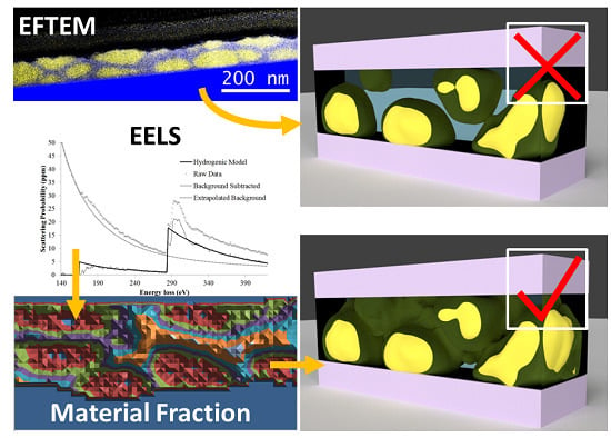
One of the drawbacks of this method is that it is a projection. A second drawback is that it is a qualitative measurement. Together, these can distort one’s perception of the actual structures in the material. Intensities are linked to a predominance of one material or another, but this says nothing about purity. For example, if one were to examine a sample and find areas of high PCBM concentration the natural interpretation would be to assume these are PCBM aggregations in a network of donor polymers. However, this same picture can be interpreted as an interconnected donor polymer web in a PCBM matrix. Without knowing purity (or the volume fraction) of each constituent polymer, these two cases become indistinguishable. EFTEM tomography alleviates the problem of projection and is thereby able to distinguish between these two cases but still lacks quantitative information about purity. This technique is also technically challenging and has seen limited use in the investigation of OPV material systems.
In this study, we explore an alternative material detection mechanism that allows for a quantitative measurement of the fraction of each material. In the first part of the paper we show how this can be accomplished, given a few assumptions, with a spectrum image that captures the carbon K edge. Using this technique we find evidence for a mixed phase in a P3HT/PCBM system. We then outline a further refinement of the technique that relies on both the carbon K edge and the sulfur L edge. With an additional measurement, fewer assumptions are required and a comparison of several calculations allows limiting the measurement errors to ±20%. Here, we illustrate the detection of a PTB7 web in a PCBM matrix rather than what initially appears to be PCBM aggregates in a PTB7 matrix.
2. Experimental Section
2.1. Materials and Device Fabrication
Two material systems were investigated in this study: P3HT/PCBM and PTB7/PCBM.
P3HT/PCBM system: Regio-regular poly(3-hexylthiophene) (P3HT) and [6,6]-phenyl C61-butyric acid methyl ester (PCBM) (99.5%) were purchased from Rieke Metals Inc. (Lincoln, NE, USA), and Nano-C Inc. (Westwood, MA, USA), respectively.
The substrates used were silicon wafers first cleaned in hot piranha (3:1 H
SO
:H
O
) at 60
C for 30 min, then washed in deionized (DI) water and dried under nitrogen gas. P3HT:PCBM (in a weight ratio of 1:0.8) was then dissolved in
o-dichlorobenzene (ODCB) to achieve a solution with P3HT and PCBM concentrations of 10 mg/mL and 8 mg/mL, respectively. Spin coating this solution on the substrate produced ∼70 nm thick films. Subsequent solvent vapor annealing in Toluene was performed for 1 h at 90% of the solvent vapor pressure to enhance phase separation. The device exhibited a
= 5.193 mA/cm
,
= 0.547 V,
= 47.8%, and a
= 1.36%. Additional details may be found in a separate publication [
12].
PTB7/PCBM system: Poly(4,8-bis[(2-ethylhexyl)oxy]benzo[1,2-b:4,5-b’]dithiophene-2,6-diyl 3-fluoro-2-[(2-ethylhexyl)carbonyl]thieno[3,4-b]thiophenediyl) (PTB7) and PCBM were purchased from 1-Material (Dorval, Qubec, Canada) and Nano-C, respectively, and used as received. The PTB7:PCBM blend solution was prepared by dissolving PTB7 and PCBM (with 1:1.5 ratio and 25 mg/mL total concentration) in dichlorobenzene and heating at 70 C for several hours.
Silicon substrates were first cleaned by detergent and subsequently sonicated in DI water, acetone, and isopropyl alcohol (IPA) followed by baking at 80
C for one hour. The poly-[(9,9-bis(3’-(
N,
N-dimethylamino)propyl)-2,7-fluorene)-alt-2,7-(9,9-dioctylfluorene)] (PFN) solution was prepared by dissolving PFN in methanol (2 mg/mL) with the presence of a small amount of acetic acid, and spun cast onto the substrates at 3000 rpm. The active layer was spun cast at 1000 rpm for 90 s followed by drying for 30 min in an inert environment. For device performance measurements, indium tin oxide (ITO) coated glass substrates were used and the device was completed by thermally depositing 8 nm of MoO
and 100 nm of Ag. The device exhibited a
= 15.3 mA/cm
,
= 0.72 V,
= 46.9%, and a
= 5.2%. Additional details may be found in a separate publication [
13].
2.2. Transmission Electron Microscopy
Transmission electron microscopy (TEM) studies were performed using a Zeiss Libra 200 MC TEM (Carl Zeiss AG: Oberkochen, Germany). This TEM is equipped with an energy filter and monochromator and was operated at an accelerating voltage of 200 kV.
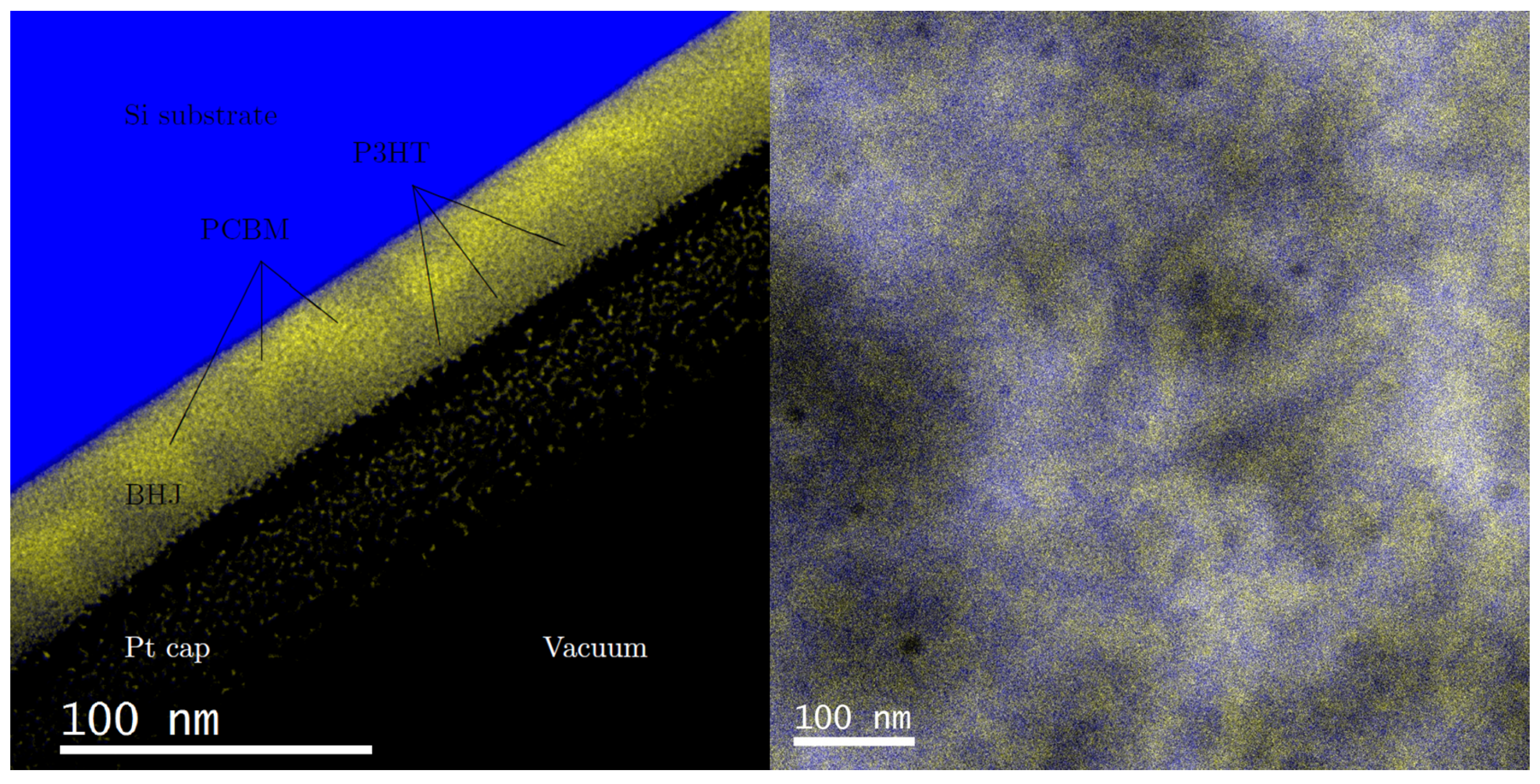
Cross-section samples were prepared using a Zeiss Auriga Crossbeam focused ion beam (FIB) microscope (Carl Zeiss AG: Oberkochen, Germany). A one micron Pt sacrificial layer was deposited over the sample surface before milling to protect the polymers. Rough milling was performed at 30 kV 2 nA to extract a lamella about 2 μm thick from the bulk sample. This lamella was mounted onto a Cu finger grid and a final polish at 10 kV 10 pA was used to thin the lamella below 100 nm.
Energy filtered TEM (EFTEM) images have previously shown successful determination of phase separation in similar bulk heterojunctions [
2,
4,
5,
6,
7]. Following the techniques described in earlier studies, EFTEM images were taken with a slit width of 8 eV centered at 19 and 30 eV. Artificial coloring was added and the EFTEM images were overlaid to enhance visualization of the phases.
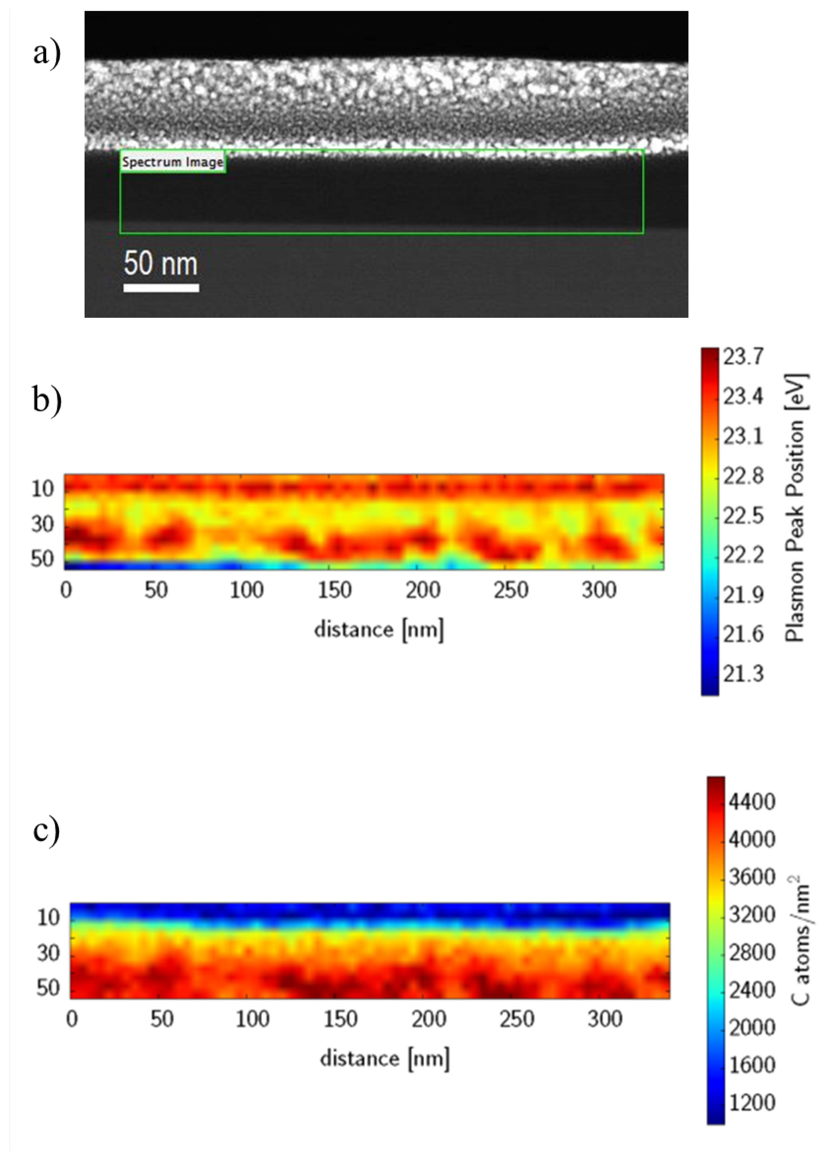
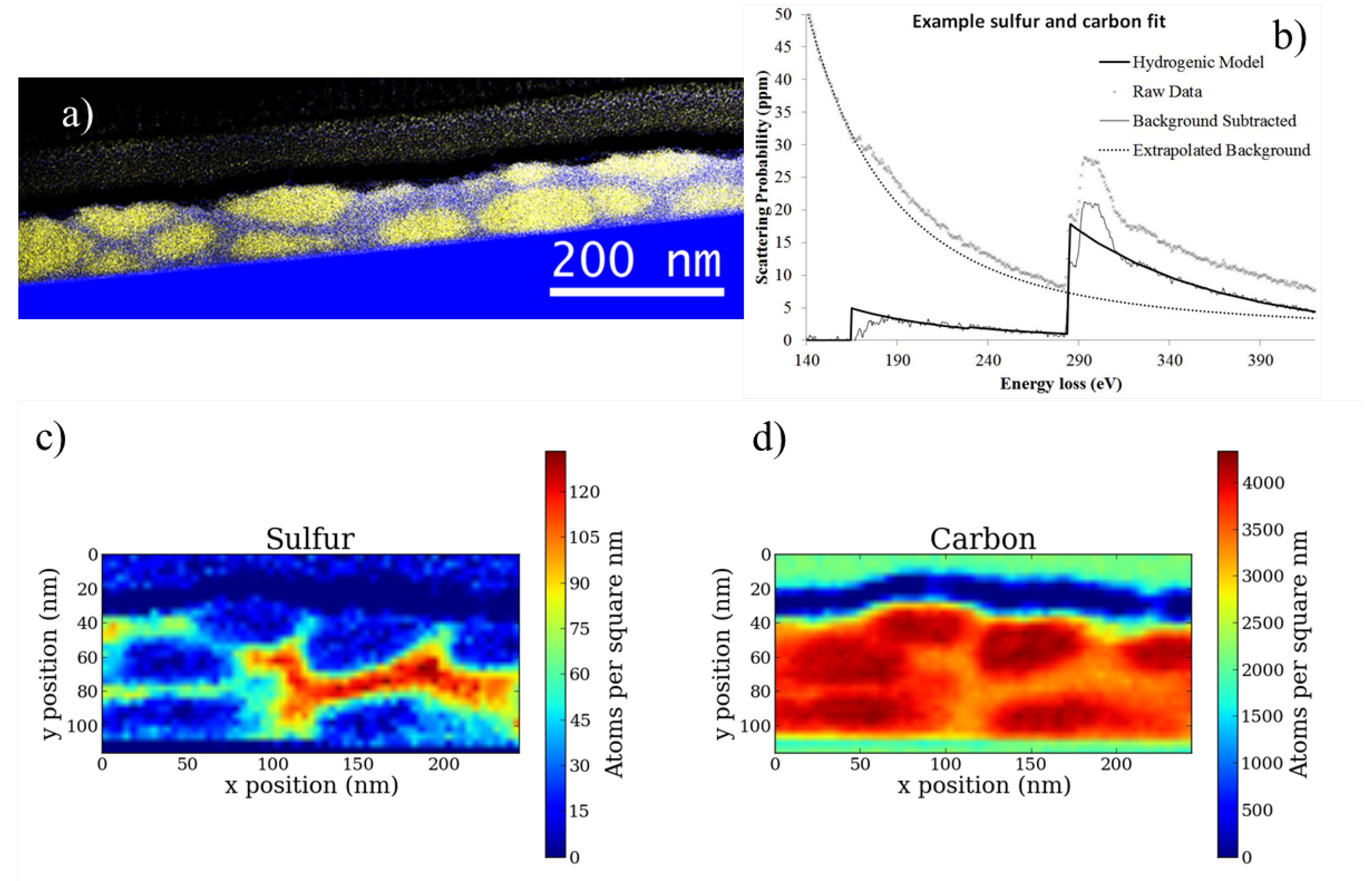
The spectrum image represented in
Figure 3 was acquired with a beam current of 48 pA, an exposure time of 0.2 s per pixel, a pixel dimension of 5 nm
with subpixel scanning and energy resolution of 0.56 eV. The convergence angle was 9 mrad and collection angle was 54 mrad. The spectrum image represented in
Figure 7 was acquired with a beam current of 18 pA, an exposure time of 0.3 s per pixel, a pixel dimension of 5 nm
with subpixel scanning and an energy resolution of 0.9 eV. The convergence angle was 9 mrad and collection angle was 30 mrad.
2.3. Data Analysis
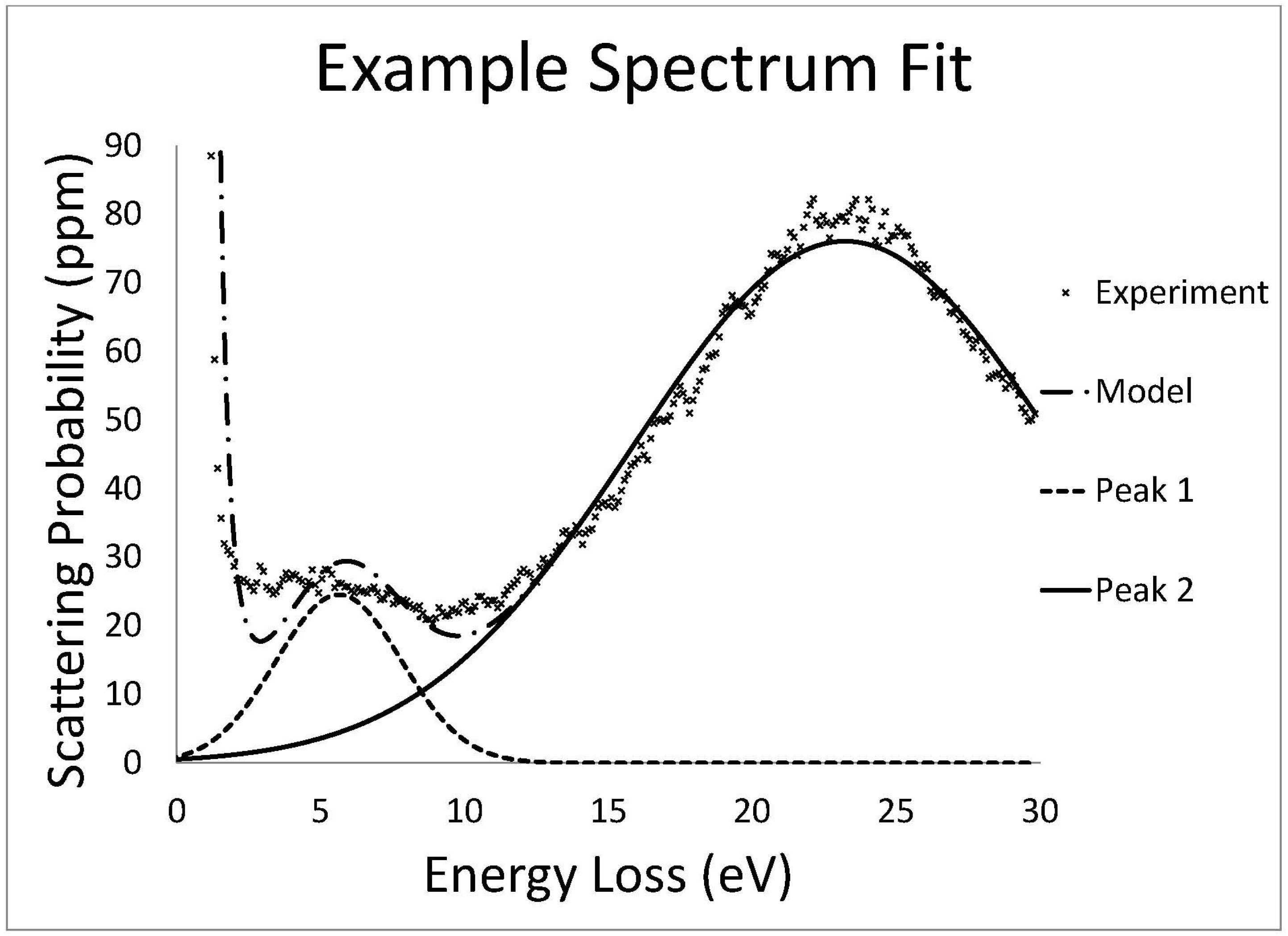
Low loss EELS data was fit with a Gaussian distribution by a least squares fitting routine. The zero loss peak (ZLP) was approximated by the sum of a Gaussian and Lorentzian distribution.
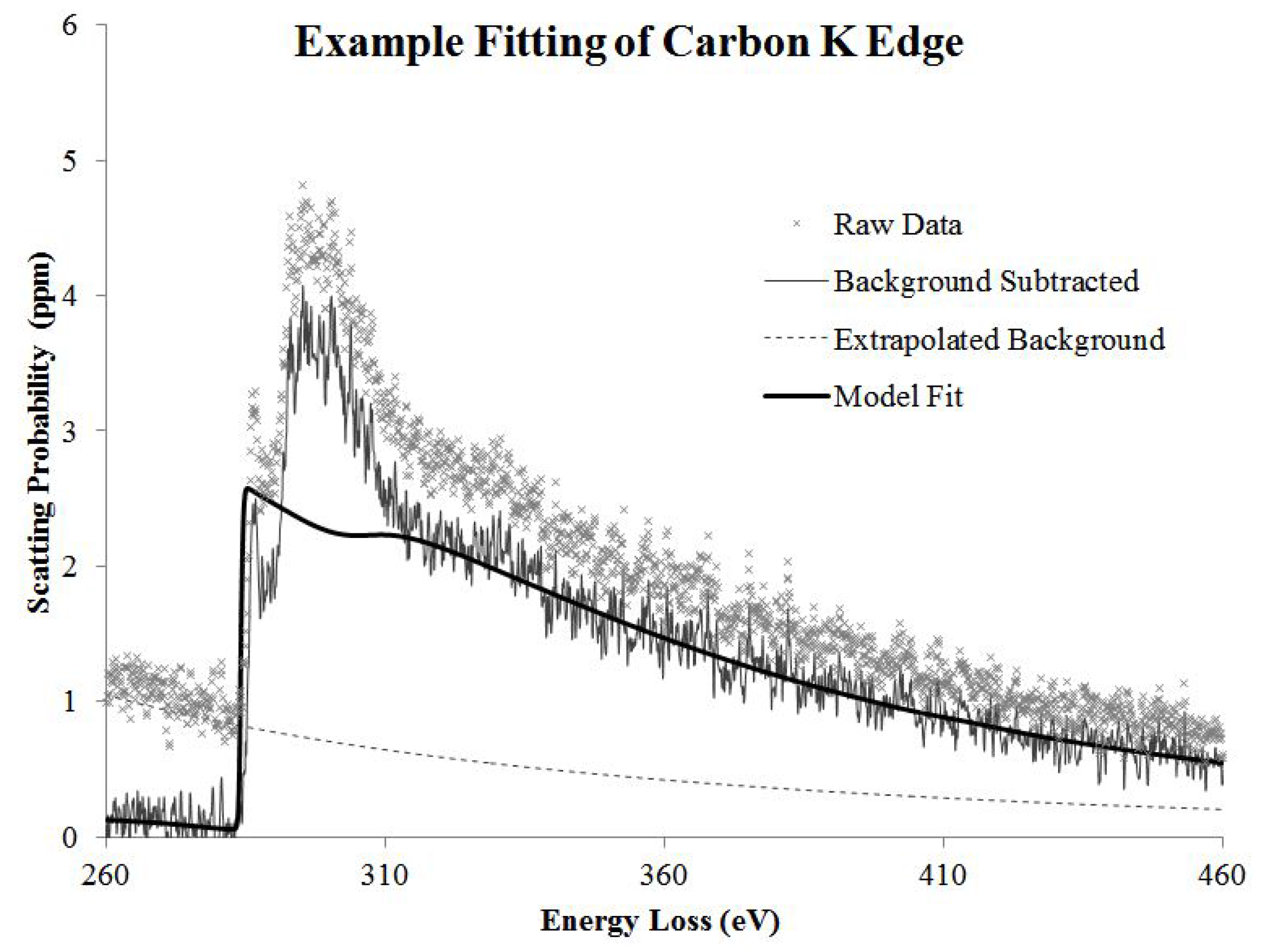
The core loss data was fit with a background subtraction routine of the form
which represents a power law decay modified by a polynomial to allow for slight deviations in the data from a true power law [
14]. Concurrently, a hydrogenic partial scattering cross section model was used to fit the core loss edges. Additionally, a representative low loss spectrum of the same area was convolved with the hydrogenic scattering cross section to more accurately fit the edge and account for features due to plural scattering.
In order to obtain quantitative elemental measurements, the scattering probability must be calculated. Once the background was subtracted from a core loss edge, the area under the edge was used as an estimate of the total scattering probability for that element. Scattering probabilities for single atoms are well known [
15] and dividing the measured scattering probability by the known scattering probability produces the number of atoms (of that element) under the beam.
Here,
is the number of atoms under the beam,
is the number of incident electrons,
is the number of scattered electrons (area under the EELS edge), and
is the probability of scattering from a single atom. For further discussion, see Egerton [
14].
4. Phase Ratio Mapping
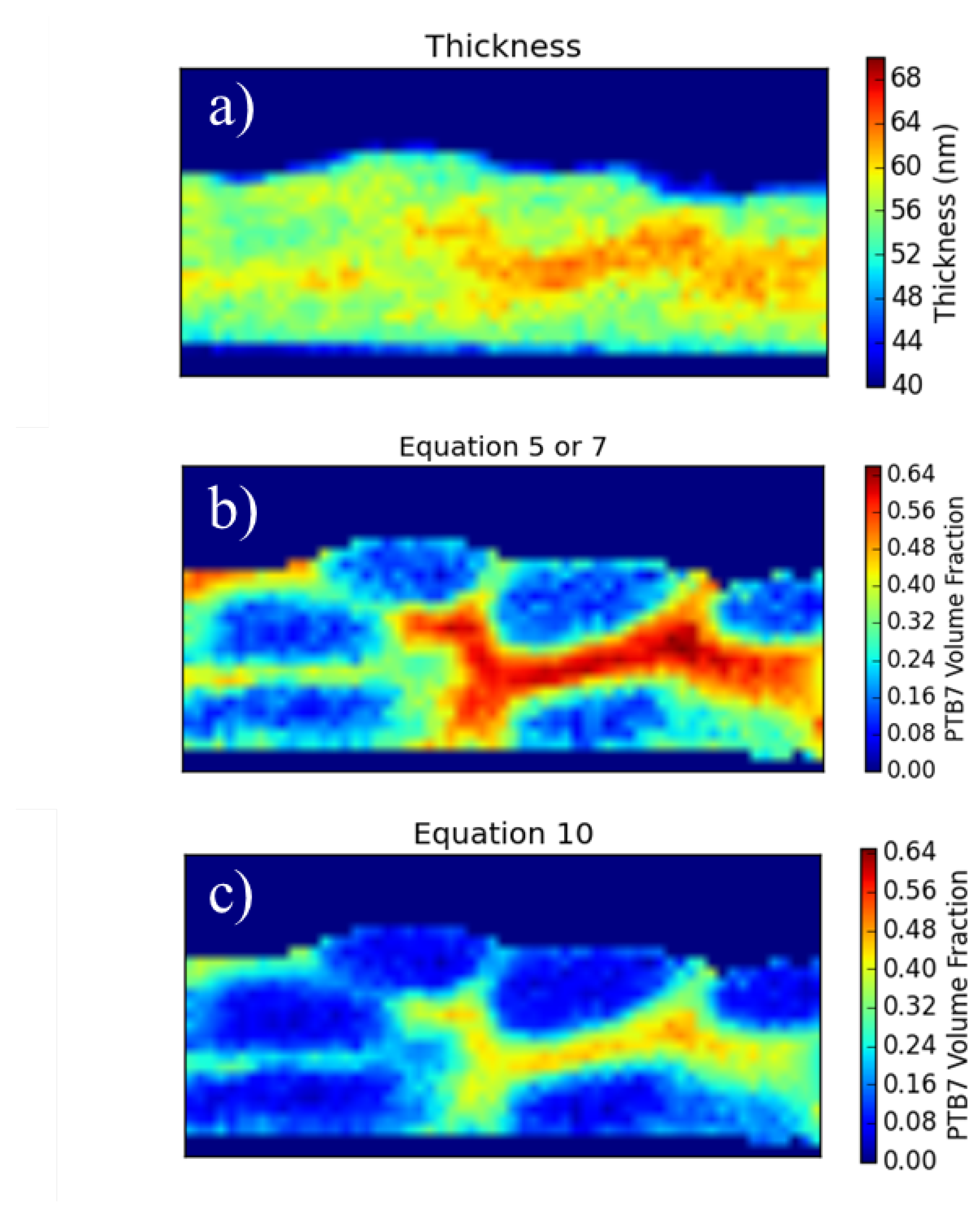
With a carbon density map a further quantification becomes possible, namely the ratio of the component materials under the beam. In order to obtain this information we must know the thickness of the sample. If we know the thickness and we know the carbon density of the materials involved, we can calculate the fraction of each component present through a linear combination of the predicted carbon density.
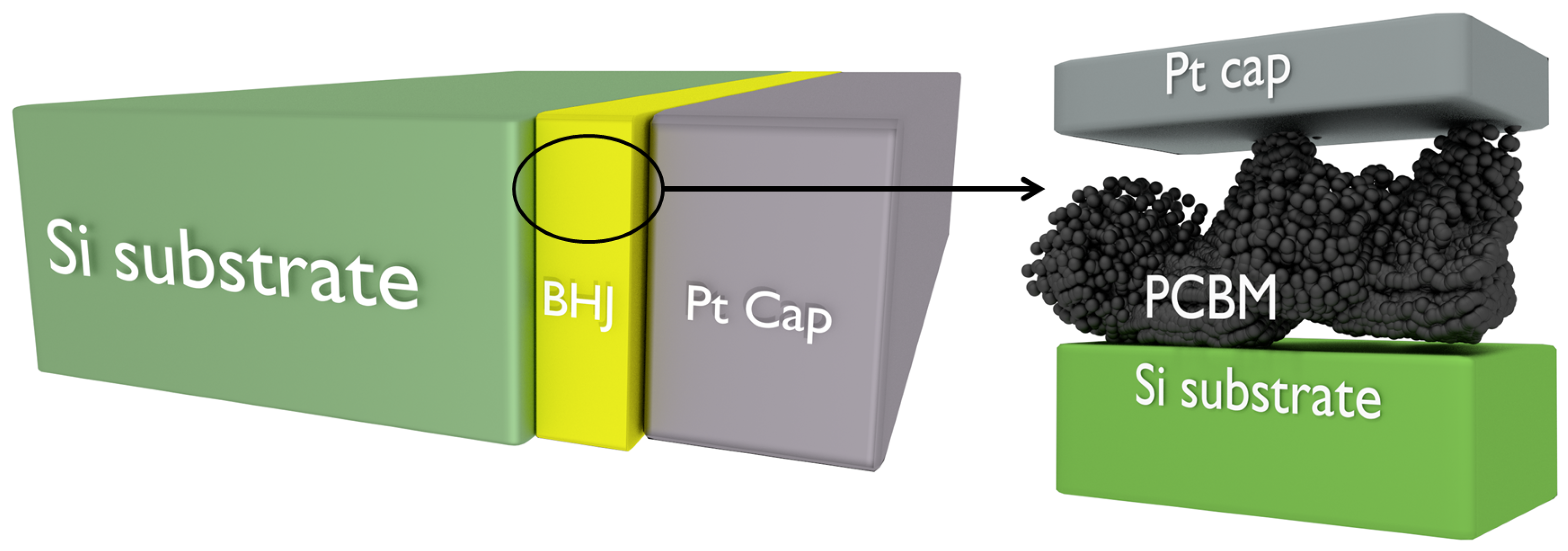
Figure 5.
Conceptual diagram to aid understanding of the equations. The left-hand diagram is oriented perpendicular to the beam which traverses the sample vertically. We assume P3HT occupies some thickness within the BHJ () and that the rest of the BHJ is occupied by PCBM (). In general, the total thickness of the sample is . In certain areas of the BHJ, however, the beam will go through either all P3HT (near the Pt cap) or all PCBM (near the Si substrate). In these cases, the total sample thickness becomes and respectively.
Let
and
be the carbon density and thickness of the P3HT, and
and
be the carbon density and thickness of the PCBM.
is then the carbon areal density we would measure for material
x. In general, our measurement,
M, is comprised of two parts:
Here, χ represents the volume fraction of P3HT and is precisely what we would like to determine at every point on the sample. The only other unknown in this equation is t, the thickness of the sample.
In order to get a measurement of t, we must meet three criteria.
The area of interest over which the spectrum image is acquired must be of uniform thickness.
In order to ensure this criterion is met as close as possible, the sample was prepared in a FIB with the specific intention of making the front and back faces coplanar, the width of the junction under examination is only about 100 nm, and Zero filtered imaging shows little thickness variation. With the addition of the sulfur signal this criterion can be removed as discussed later.
There are some areas of pure material.
This criterion is rather restrictive. It requires that the feature sizes within the junction (i.e., the phase separated domain sizes) are at least as large as the thickness of the sample. This requires large domain sizes which are not representative of the ideal OPV structure. Many samples investigated did not meet this criterion and could not be analyzed with this first method. With the addition of the sulfur signal this assumption can be removed as discussed later.
The sample is contamination free.
Naturally, any contamination build-up during data acquisition will alter the carbon signal. We acquired images before and after the EELS acquisition to verify that contamination was not present.
If these three criterion are met, then in the areas of highest and lowest carbon concentration, Equation (
2) simplifies since
χ is either 0 or 1 (making use of the presence of pure material). The areas with the highest carbon density are pure PCBM while the areas with the lowest carbon density are pure P3HT. This is expressed as:
and,
where
and
are the measured areal densities of the highest and lowest value pixels within the junction (
i.e., taken from the data in
Figure 3b in locations where the beam is actually within the junction not on the Pt cap). We can then use the literature densities and our measurements to obtain the sample thickness. If the three criterion are indeed met, we should find that
. Indeed we find from the pure PCBM regions a thickness value of 65 nm and from the pure P3HT regions a thickness value of 66 nm. Their close agreement indicates that the criterion were met acceptably well.
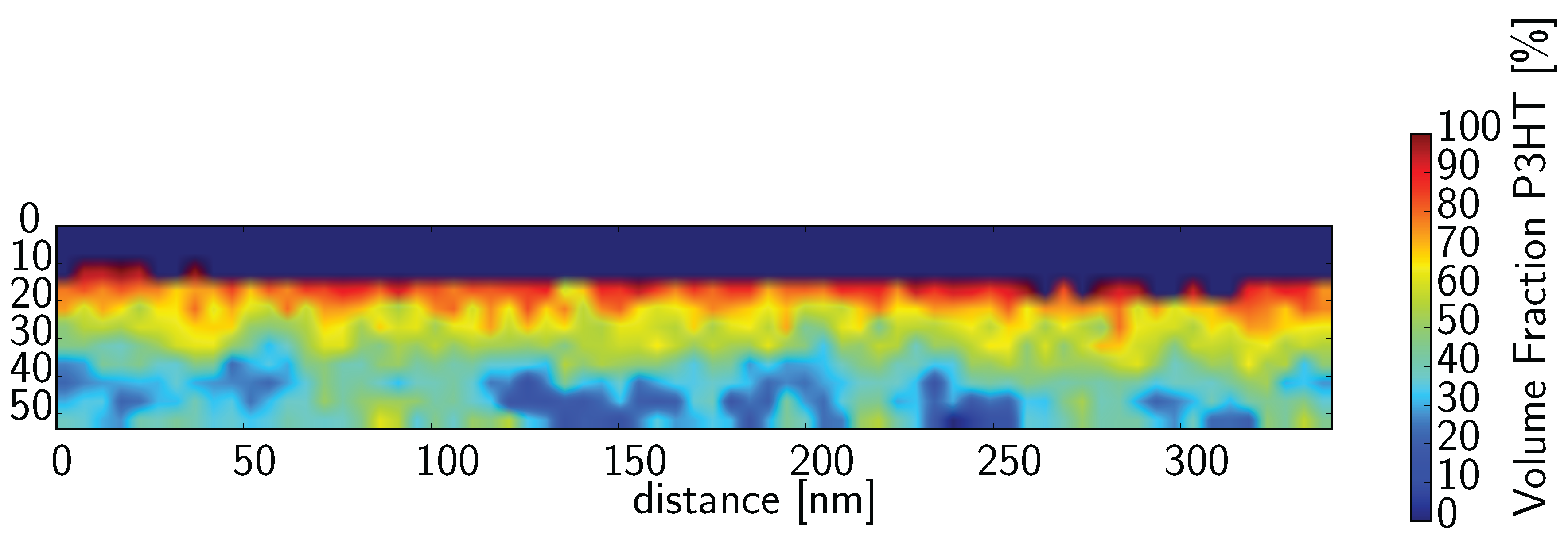
Taking the thickness of the sample to be 65 nm (changing the sample thickness from 65 to 66 nm does not lead to any significant change in the result) the carbon density map (
Figure 3b) can be re-interpreted as a phase ratio map by solving Equation (
2) for
χ and inserting the measured carbon areal densities into
M:
Figure 6 shows the carbon densities re-interpreted as a fraction of P3HT. What we immediately see from this picture is that we have a large amount of mixed material that is always present between the pure phases. There are three possibilities that may account for this. The first possibility is that the transition region from one material to the other is not perpendicular to the electron beam which will make a sharp transition appear much smoother. This option, although possible, seems unlikely since we do not see a sharp transition anywhere. If the mixed material was simply due to overlapping domains, we would expect to get a sharp transition somewhere. Alternatively, fractal-like structure with well defined (sharp) boundaries yet decreasing in feature size could also produce a similar component profile. The third possibility, which may not actually be much different from the second except in how it is expressed, is that there is a mixed phase composed of both P3HT and PCBM. There is mounting evidence that such a mixed phase exists [
7,
24,
25,
26]. Treat
et al. (2011) [
26] observed quick diffusion of PCBM into the amorphous areas of P3HT, suggesting that, though crystalline P3HT is immiscible with PCBM, amorphous P3HT readily mixes upon heating. Pfannmöller
et al. (2011) [
7] observed such a mixed phase employing EFTEM imaging and a nonlinear multivariate statistical analysis. They found that the mixed phase decreases device performance due to a decrease in charge separation. Tvingstedt
et al. (2010) [
25], and Zhang
et al. (2012) [
24] also uncovered evidence for the presence and detriment of a mixed phase through the use of photoluminescent spectroscopy and near-infrared femtosecond transient absorption spectroscopy. Therefore it seems most likely that what we are observing in
Figure 6 is a mixed phase between the pure domains of P3HT and PCBM.
In
Figure 6, the average P3HT fraction is 0.536. This is quite close to the value expected based on our fabrication parameters of 0.555.
Figure 6.
Data from
Figure 3b re-interpreted as a fraction of P3HT. In some areas Equation (
5) produces false values (above 100%) due to the low carbon concentration in the Pt cap toward the top. In these cases, it is not a physical result. These values have been set to zero.
Figure 6.
Data from
Figure 3b re-interpreted as a fraction of P3HT. In some areas Equation (
5) produces false values (above 100%) due to the low carbon concentration in the Pt cap toward the top. In these cases, it is not a physical result. These values have been set to zero.
6. Conclusions
We have shown two methods for component material detection in OPV systems, namely EELS imaging for plasmon peak position mapping and EELS imaging for core loss elemental concentration mapping. The plasmon peak position mapping relies on plasmon position shifts that are well established for EFTEM imaging but, to the author’s knowledge, no quantitative position mapping across a sample has been done. Such a map gives slightly more detailed information about the sample because each spectrum can be analyzed independently post-acquisition for possible artifacts.
EELS image analysis for quantitative carbon and sulfur concentration mapping demonstrated component detection capabilities due to the elemental density differences between P3HT and PTB7, and PCBM.
We further demonstrated that the carbon areal density map may be transformed into a component ratio map which offers a much more useful quantification of the data. This requires that the sample thickness be known, which we demonstrated can be obtained from the carbon areal density map with a few assumptions, or from the combined carbon and sulfur areal densities. The component ratio map may be employed to determine the sharpness of the component separation as well as the purity of the separated phases which will have significant impact on device performance.
The ability to interpret core loss EELS images in terms of absolute atomic density has much farther-reaching applications than just OPV characterization. It could be used in studies on block copolymers, ionomers, or other biological samples. It could be used to determine impurity concentrations, atomic ratios, or ratios of composite materials. Moreover, once the data is converted to atomic density, rather than counts, different experiments under different conditions in different microscopes may be compared to each other.


 ,
, 


