Towards High Performance Organic Photovoltaic Cells: A Review of Recent Development in Organic Photovoltaics


Abstract
:
1. Introduction

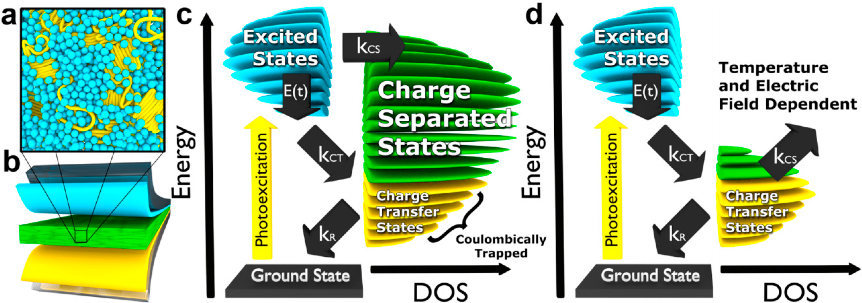
2. Photophysics Mechanism
2.1. Hot Exciton Dissociation


2.2. Spin Nature of CT States

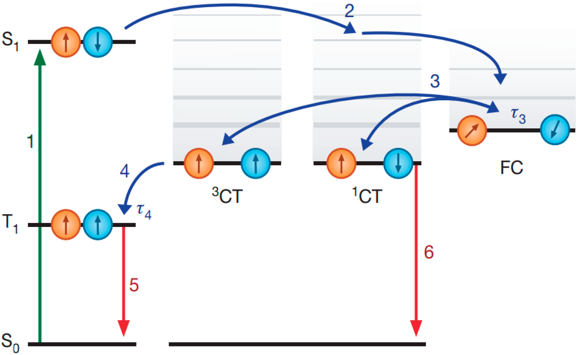
2.3. Charge Separated States

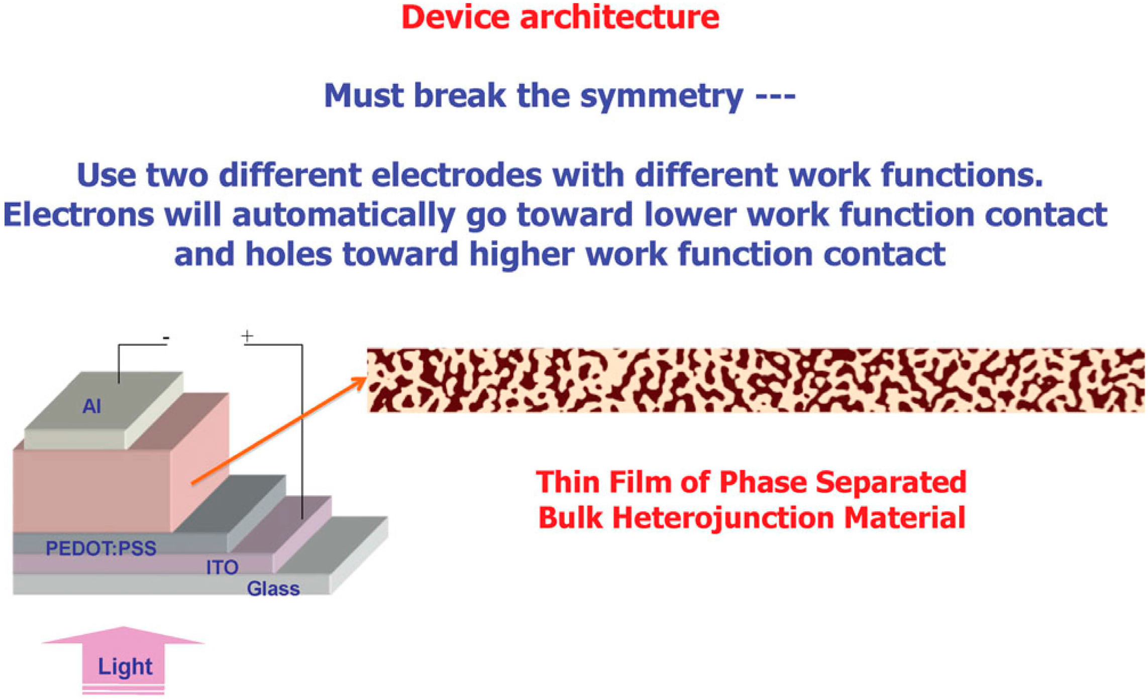
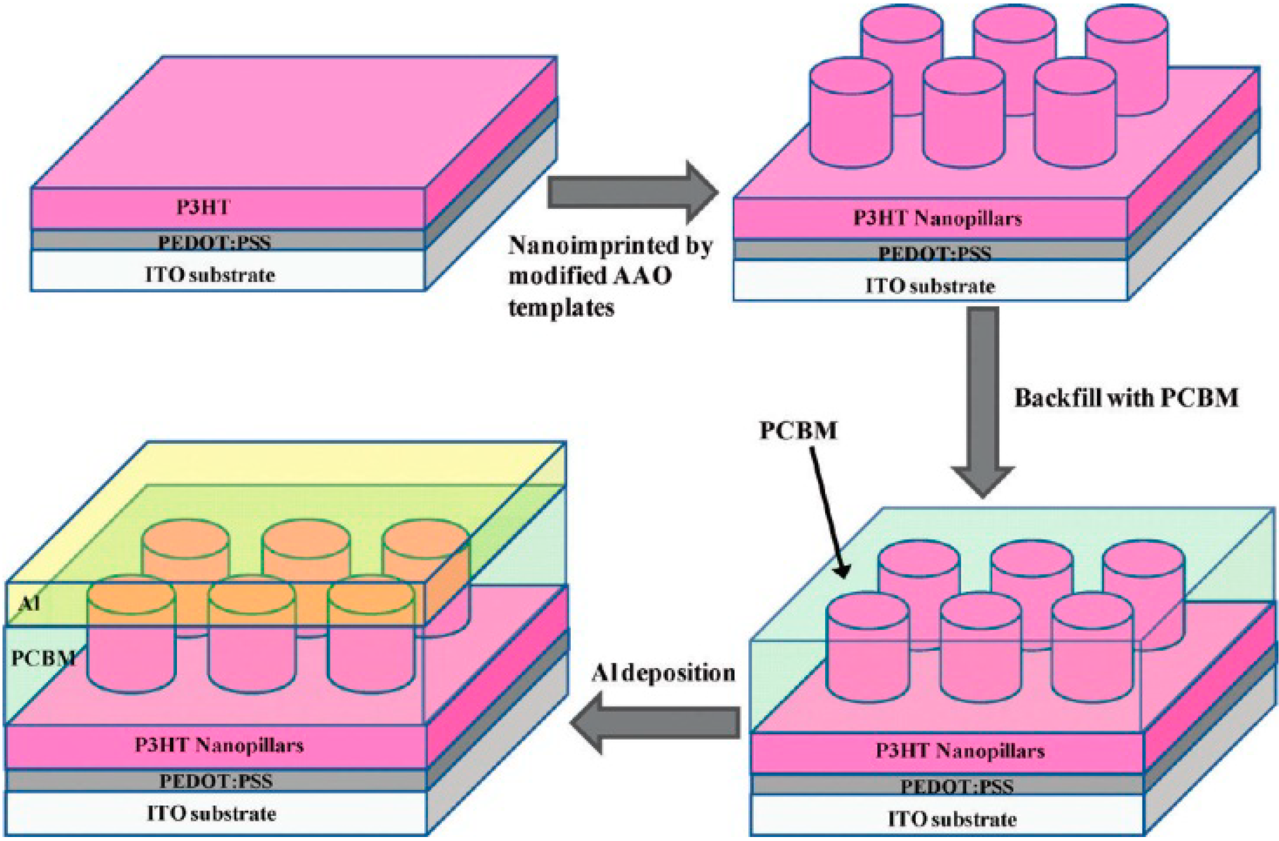
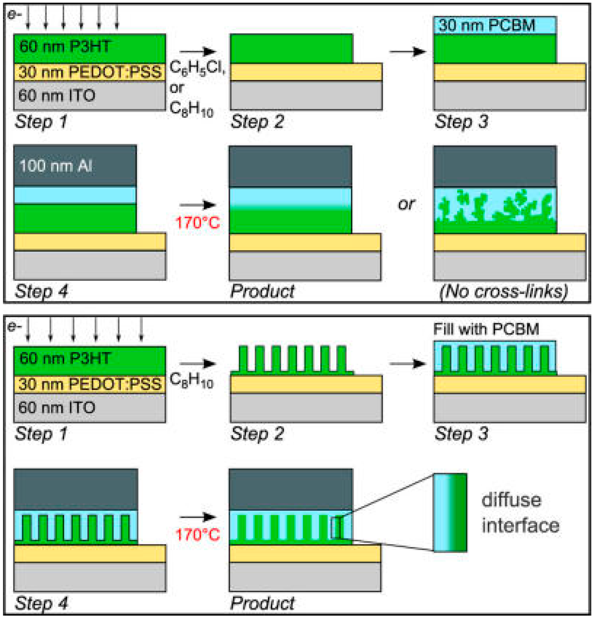
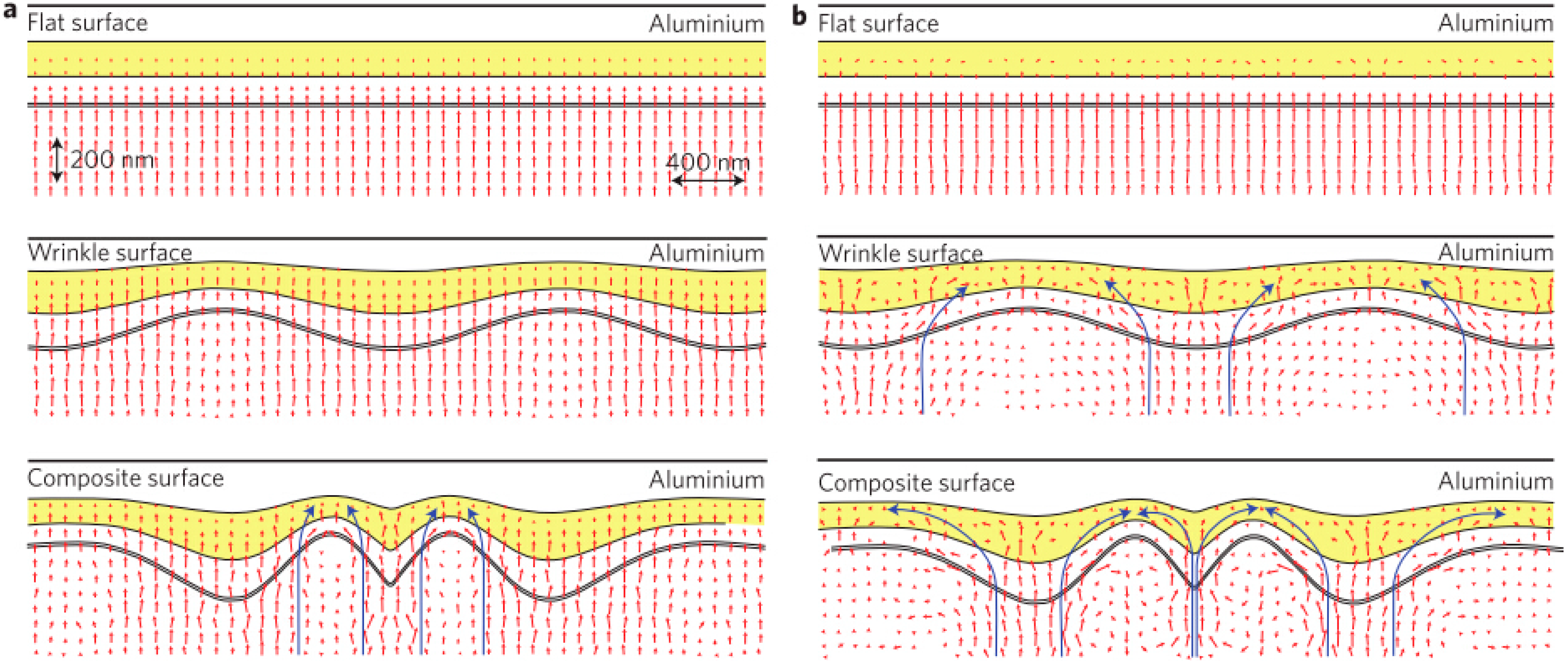
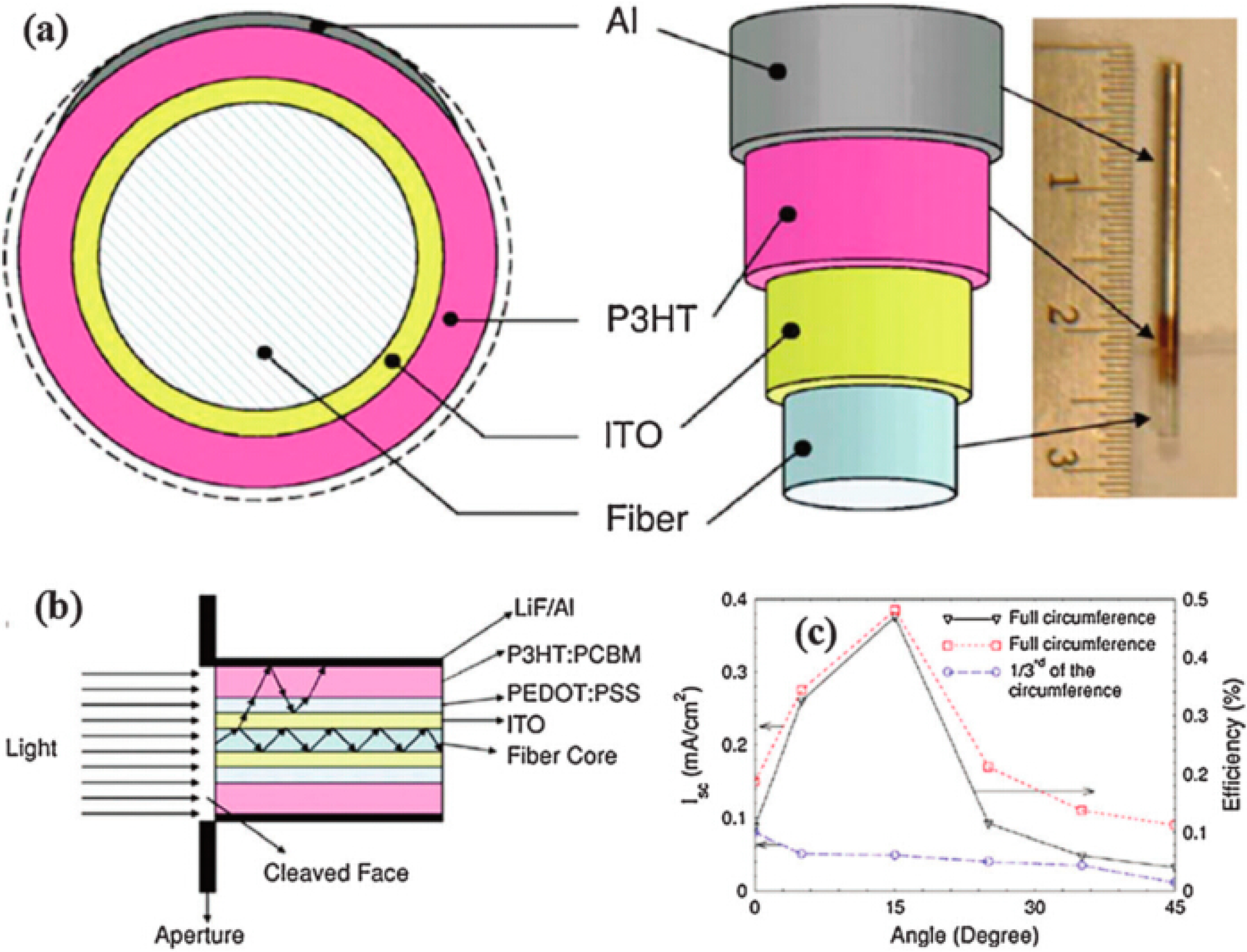
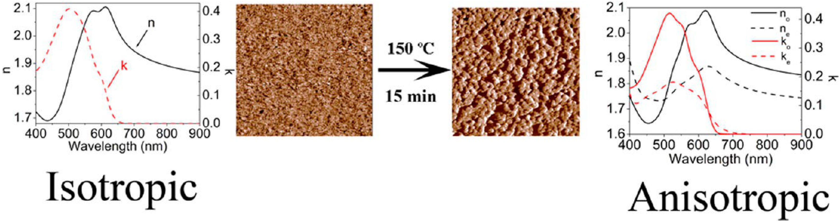
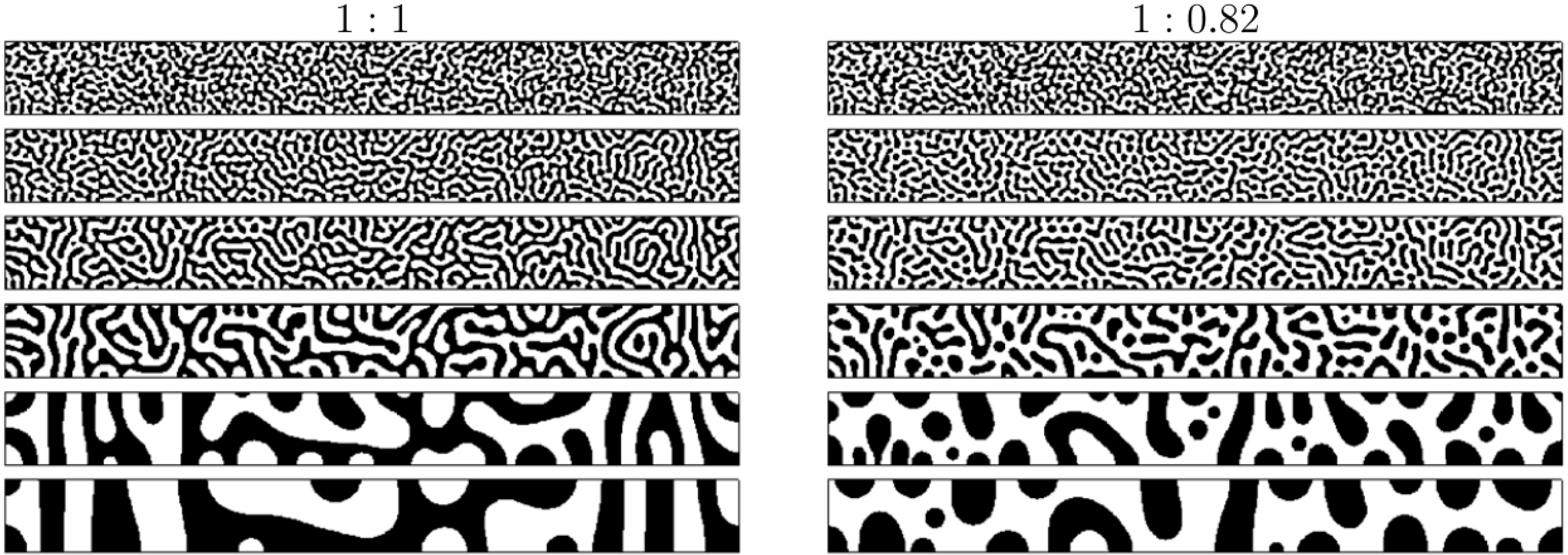
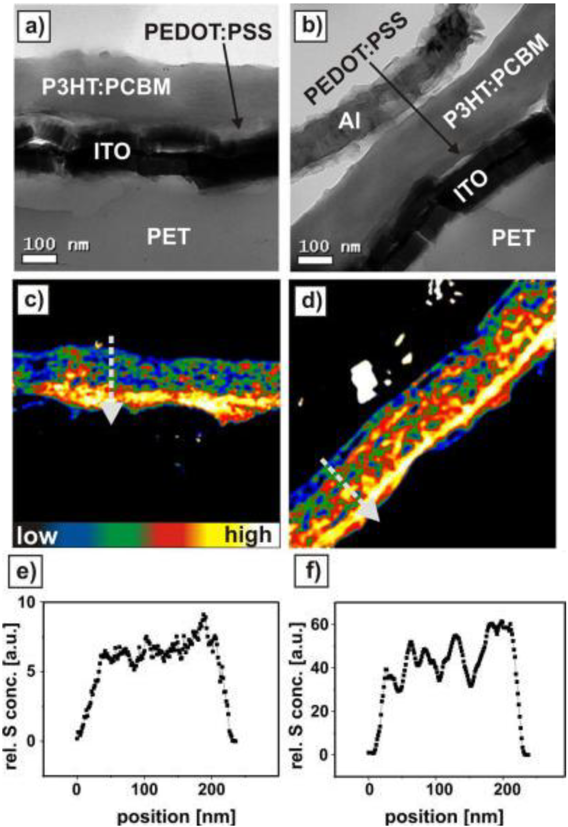
3. OPV Structure Design


4. Approaches for Further Increasing PCE
4.1. Thermal Annealing


4.2. Polar Solvent Annealing

| Solvents | Methods | Active Layer | VOC (V) | JSC (mA/cm2) | FF (1) | PCE (%) | Ref. |
|---|---|---|---|---|---|---|---|
| Methanol (ME) | Direct exposure | P3HT/PC60BM | 0.63 | 9.40 | 0.52 | 2.9 | [138] |
| Ethanol | Direct exposure | P3HT/PC60BM | 0.64 | 10.20 | 0.56 | 3.25 | [138] |
| Propanol | Direct exposure | P3HT/PC60BM | 0.64 | 9.26 | 0.47 | 2.7 | [138] |
| Butanol | Direct exposure | P3HT/PC60BM | 0.64 | 9.27 | 0.45 | 2.76 | [138] |
| Methanol | Solvent annealing | PTB7/PC70BM | 0.72 | 14.69 | 0.73 | 7.72 | [144] |
| Ethanol (EA) | Solvent annealing | PTB7/PC70BM | 0.72 | 14.75 | 0.72 | 7.65 | [144] |
| 2-ME | Solvent annealing | PTB7/PC70BM | 0.71 | 14.45 | 0.71 | 7.28 | [144] |
| 2-ME + EA (1%) | Solvent annealing | PTB7/PC70BM | 0.71 | 16.76 | 0.73 | 8.69 | [144] |
| Methanol | Solvent annealing | PTB7/PC70BM (Al cathode) | 0.75 | 13.92 | 0.68 | 7.20 | [143] |
| Methanol | Solvent annealing | PTB7/PC70BM (Ca/Al cathodes) | 0.76 | 15.46 | 0.68 | 7.94 | [143] |
| Chlorobenzene (CB) | Solvent annealing | PBDTTPD/PC70BM | 0.88 | 9.11 | 0.61 | 4.92 | [145] |
| DCB | Solvent annealing | PBDTTPD/PC70BM | 0.89 | 10.52 | 0.53 | 4.99 | [145] |
| DCB | Solvent annealing | p-phenylenevinylene copolymer/PC70BM | 0.81 | 6.32 | 0.55 | 2.80 | [146] |
| Chloroform (CF) | SVA | PCDTBT/PC70BM | 0.87 | 15.65 | 0.52 | 7.03 | [147] |
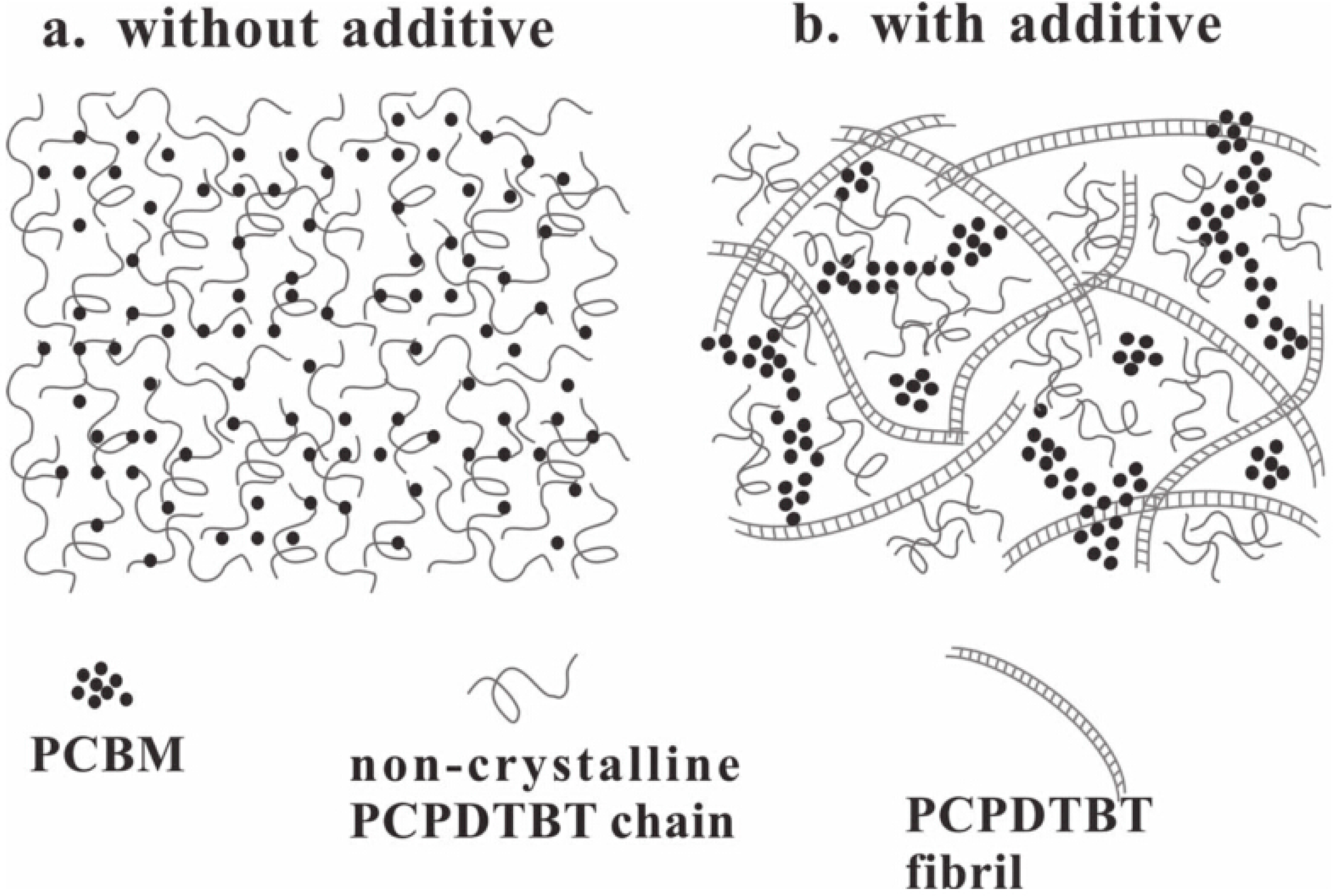
4.3. Additive
| Additives | Vol (%) | Solvent | Active Layer | VOC (V) | JSC (mA/cm2) | FF (1) | PCE (%) | Ref. |
|---|---|---|---|---|---|---|---|---|
| DIO | 3 | CF | BDT-DPP/PC70BM | 0.76 | 8.49 | 0.60 | 3.88 | [176] |
| DIO | 7 | ODCB | BDT-DPP/PC70BM | 0.72 | 11.86 | 0.61 | 5.29 | [176] |
| DIO | 2.5 | - | PCPDTBT/PC70BM | 0.62 | 14.90 | 0.50 | 4.62 | [158] |
| DIO | 3 | - | PBDTBDD/Bis-PCBM | 1.00 | 10.02 | 0.61 | 6.07 | [159] |
| DIO | 3 | - | PBDTFBZS/PC70BM | 0.88 | 12.03 | 0.71 | 7.74 | [177] |
| DIO | 3 | ODCB | PBDTTPD/PC70BM | 0.87 | 6.6 | 0.55 | 3.2 | [165] |
| CN | 4 | ODCB | PBDTTPD/PC70BM | 0.85 | 9.4 | 0.59 | 4.7 | [165] |
| CN + DIO | 10 + 1 | ODCB | PBDTTPD/PC70BM | 0.87 | 11.0 | 0.67 | 6.4 | [165] |
| CN + DIO | 4 + 1 | CB | PBDTTPD/PC70BM | 0.93 | 10.89 | 0.70 | 7.1 | [165] |
| MeN + DIO | 2 + 3 | Xylenes | PDTSTPD/PC70BM | 0.89 | 11.7 | 0.60 | 6.2 | [178] |
| ODT | 2.5 | - | PCPDTBT/PC70BM | 0.61 | 14.39 | 0.44 | 3.87 | [158] |
| DCO | 2.5 | - | PCPDTBT/PC70BM | 0.63 | 11.80 | 0.46 | 3.45 | [158] |
| BrAni | 1 | - | P3HT/PC60BM | 0.63 | 11.16 | 0.59 | 4.15 | [171] |
| BrAni | 2 | - | N(Ph-2T-DCN-Et)3/PC70BM | 0.96 | 7.81 | 0.50 | 3.60 | [170] |
| P6 | 0.25 | - | P3HT/PC60BM | 0.60 | 12.2 | 0.53 | 3.78 | [169] |
| F4-TCNQ | 0.004 | - | PCDTBT/PC70BM | 0.90 | 14.0 | 0.63 | 7.94 | [172] |
| N-MCNTs | 1.5 | - | PTB7/PC70BM | 0.7 | 17.4 | 0.69 | 8.41 | [173] |
| SQ | 1 | - | P3HT/PC60BM | 0.60 | 11.6 | 0.65 | 4.51 | [167] |
| DPSQ | 5 | - | P3HT/PC60BM | 0.61 | 8.9 | 0.68 | 3.65 | [168] |
| Me-naph | 2 | Toluene | PIDT-phanQ/PC70BM | 0.87 | 10.8 | 0.65 | 6.1 | [179] |
| Me-naph | 2 | o-Xylene | PIDT-phanQ/PC70BM | 0.86 | 10.5 | 0.63 | 5.7 | [179] |
| DTDBAL | 0.05 | - | P3HT/PC60BM | 0.66 | 10.58 | 0.52 | 3.60 | [174] |
| DPP-CN | 8 | CN/THF | P3HT/PC60BM | 0.66 | 12.29 | 0.58 | 4.70 | [180] |
| PVK | 13 | - | P3HT/IC60BA | 0.78 | 9.1 | 0.50 | 3.5 | [175] |
| PCBTTE | 5 | - | P3HT/PC60BM | 0.61 | 11.06 | 0.65 | 4.37 | [181] |
5. Conclusions and Outlook
- (i)
- It is part of a trend to apply an apparatus with a capability of capturing the motion trail of charge carriers at the femtosecond level for the characterization of the photophysical process in OPV. With the advance in characterization techniques, the mechanism of charge transfer could be more clearly understood, leading to the better design and synthesis of organic functional materials with low-bandgap and strong near-infrared absorption;
- (ii)
- The design of a novel device architecture is an efficient way for improving the PCE. To break the limit of conventional thin film BHJ, there have been several new architectures, e.g., wrinkled surface, wire-shape OPV and nanostructured OPV, to be realized to trap more incident light and to pave the way for more efficient charge transfer. The future work in this area should be focused on designing large-scale compatible and low-cost processable architecture;
- (iii)
- Post modification is a convenient method to benefit the device performance directly. The general annealing, including solvent annealing and thermal annealing, is also effective with respect to the new synthesized materials. However, the mechanism of these conventional annealing process is still unclear. With the development of characterization methods, much effort should be made on the illustration of these modifications for more precise control. Moreover, there is a large amount of novel modification that can be incorporated to make a contribution toward high device performance, e.g., soaking method, doping additives and inversing methods.
Acknowledgments
Author Contributions
Conflicts of Interest
References
- Gan, Q.; Bartoli, F.J.; Kafafi, Z.H. Plasmonic-enhanced organic photovoltaics: Breaking the 10% efficiency barrier. Adv. Mater. 2013, 25, 2385–2396. [Google Scholar] [CrossRef] [PubMed]
- Green, M.A.; Emery, K.; Hishikawa, Y.; Warta, W.; Dunlop, E.D. Solar cell efficiency tables. Prog. Photovolt. Res. Appl. 2012, 20, 12–20. [Google Scholar] [CrossRef]
- Green, M.A. Recent developments in photovoltaic. Sol. Energy 2004, 76, 3–8. [Google Scholar] [CrossRef]
- Bauhuis, G.J.; Mulder, P.; Haverkamp, E.J.; Huijben, J.C.C.M.; Schermer, J.J. 26.1% thin-film GaAs solar cell using epitaxial lift-offs. Sol. Energ. Mater. Sol. Cells 2009, 93, 1488–1491. [Google Scholar] [CrossRef]
- Contreras, M.A.; Egaas, B.; Ramanathan, K.; Hiltner, J.; Swartzlander, A.; Hasoon, F.; Noufi, R. Progress toward 20% efficiency in Cu(In,Ga)Se2 polycrystalline thin-film solar cells. Prog. Photovoltaics 1999, 7, 311–316. [Google Scholar] [CrossRef]
- Romeo, A.; Terheggen, A.; Abou-Ras, D.; Batzner, D.L.; Haug, F.J.; Kalin, M.; Rudmann, D.; Tiwari, A.N. Development of thin-film Cu(In,Ga)Se2 and CdTe solar cells. Prog. Photovoltaics 2004, 12, 93–111. [Google Scholar]
- Solar PV Manufacturing Cost Analysis. Available online: http://www.nrel.gov/analysis/key_activities_jobs_pv_mfg_cost.html (accessed on 10 October 2011).
- Dou, L.; You, J.; Hong, Z.; Xu, Z.; Li, G.; Street, R.A.; Yang, Y. A decade of organic/polymeric photovoltaic research. Adv. Mater. 2013, 25, 6642–6671. [Google Scholar] [CrossRef] [PubMed]
- Zhou, N.J.; Buchholz, D.B.; Zhu, G.; Yu, X.G.; Lin, H.; Facchetti, A.; Marks, T.J.; Chang, R.P.H. Ultraflexible polymer solar cells using amorphous zinc-indium-tin oxide transparent electrodes. Adv. Mater. 2014, 26, 1098–1104. [Google Scholar] [CrossRef] [PubMed]
- Zhao, J.; Liu, L.; Wu, J.; Yu, J.S. Spectral variation of solution-processed blue bis[(4,6-difluorophenyl)-pyridinato-N,C2'] (picolinate) iridium(III) phosphor. Dyes Pigments 2014, 102, 234–241. [Google Scholar] [CrossRef]
- Huang, J.; Wang, H.Y.; Qi, Y.G.; Yu, J.S. Influence of bias voltage and temperature on charge transfer states in organic photovoltaic and electroluminescent integrated device. Appl. Phys. Lett. 2011, 104, 203301. [Google Scholar]
- Li, G.; Zhu, R.; Yang, Y. Polymer solar cells. Nat. Photonics 2012, 6, 153–161. [Google Scholar] [CrossRef]
- You, J.; Dou, L.; Yoshimura, K.; Kato, T.; Ohya, K.; Moriarty, T.; Emery, K.; Chen, C.; Gao, J.; Li, G.; et al. A polymer tandem solar cell with 10.6% power conversion efficiency. Nat. Commun. 2013, 4, 1446. [Google Scholar]
- Clarke, T.M.; Durrant, J.R. Charge photogeneration in organic solar cells. Chem. Rev. 2010, 110, 6736–6767. [Google Scholar] [CrossRef] [PubMed]
- Janssen, R.A.J.; Nelson, J. Factors limiting device efficiency in organic photovoltaics. Adv. Mater. 2013, 25, 1847–1858. [Google Scholar] [CrossRef]
- Bakulin, A.A.; Martyanov, D.S.; Paraschuk, D.Y.; Pshenichnikov, M.S.; van Loosdrecht, P.H.M.J. Ultrafast charge photogeneration dynamics in ground-state charge-transfer complexes based on conjugated polymers. J. Phys. Chem. B 2008, 112, 13730. [Google Scholar] [CrossRef] [PubMed]
- Zhou, N.J.; Lin, H.; Lou, S.J.; Yu, X.G.; Guo, P.J.; Manley, E.F.; Loser, S.; Hartnett, P.; Huang, H.; Wasielewski, M.R.; et al. Morphology-performance relationships in high-efficiency all-polymer solar cells. Adv. Energy Mater. 2014. [Google Scholar] [CrossRef]
- Guo, X.G.; Zhou, N.J.; Lou, S.J.; Smith, J.; Tice, D.B.; Hennek, J.W.; Ortiz, R.P.; Navarrete, J.T.L.; Li, S.Y.; Strzalka, J. Polymer solar cells with enhanced fill factors. Nat. Photonics 2013, 7, 825–833. [Google Scholar] [CrossRef]
- Wang, H.Y.; Zheng, Y.F.; Zhang, L.; Yu, J.S. Effect of two-step annealing on the performance of ternary polymer solar cells based on P3HT:PC71BM:SQ. Sol. Energ. Mater. Sol. Cells 2014, 128, 215–220. [Google Scholar] [CrossRef]
- Antoniadis, H.; Hsieh, B.R.; Abkowitz, M.A.; Jenekhe, S.A.; Stolka, M. Photovoltaic and photoconductive properties of aluminum/poly(p-phenylene vinylene) interface. Synthetic Met. 1994, 62, 265–271. [Google Scholar] [CrossRef]
- Riess, W.; Karg, S.; Dyakonov, V.; Meier, M.; Schwoerer, M. Electroluminescence and photovoltaic effect in PPV Schottky diodes. J. Lumin. 1994, 60, 906–911. [Google Scholar]
- Hoppe, H.; Sariciftci, N.S. Organic solar cells: An overview. J. Mater. Res. 2004, 19, 1924–1945. [Google Scholar] [CrossRef]
- Tang, C.W. Two-layer organic photovoltaic cell. Appl. Phys. Lett. 1986, 48, 183–185. [Google Scholar] [CrossRef]
- Sariciftci, N.S.; Smilowitz, L.; Heeger, A.J.; Wudl, F. Photoinduced electron transfer from a conducting polymer to buckminsterfullerene. Science 1992, 258, 1474–1476. [Google Scholar] [CrossRef] [PubMed]
- Morita, S.; Zakhidov, A.A.; Yoshino, K. Doping effect of buckminsterfullerene in conducting polymer: Change of absorption spectrum and quenching of luminescene. Solid State Commun. 1992, 82, 249–252. [Google Scholar] [CrossRef]
- Sariciftci, N.S.; Smilowitz, L.; Heeger, A.J.; Wudl, F. Semiconducting polymers (as donors) and buckminsterfullerene (as acceptor): Photoinduced electron transfer and heterojunction device. Synthetic Met. 1993, 59, 333–352. [Google Scholar] [CrossRef]
- Yu, G.; Gao, J.; Hummelen, J.C.; Wudl, F.; Heeger, A.J. Polymer photovoltaic cells: Enhanced efficiencies via a network of internal donor-acceptor heterojunctions. Science 1995, 270, 1789–1791. [Google Scholar] [CrossRef]
- Halls, J.J.M.; Walsh, C.A.; Greenham, N.C.; Marseglia, E.A.; Friend, R.H.; Moratti, S.C.; Holmes, A.B. Efficient photodiodes from interpenetrating polymer network. Nature 1995, 376, 498–500. [Google Scholar] [CrossRef]
- Kim, Y.J.; Lee, K.; Coates, N.E.; Moses, D.; Nguyen, T.Q.; Dante, M.; Heeger, A.J. Efficient tandem polymer solar cells fabricated by all-solution processing. Science 2007, 317, 222–225. [Google Scholar] [CrossRef] [PubMed]
- Po, R.; Carbonera, C.; Bernardi, A.; Camaioni, N. The role of buffer layers in polymer solar cells. Energ. Environ. Sci. 2011, 4, 285–210. [Google Scholar] [CrossRef]
- Carle, J.E.; Andersen, T.R.; Helgesen, M.; Bundgaard, E.; Jorgensen, M.; Krebs, F.C. A laboratory scale approach to polymer solar cells using one coating/printing machine, flexible substrates, no ITO, no vacuum and no spincoating. Sol. Energ. Mater. Sol. Cells 2013, 108, 126–128. [Google Scholar] [CrossRef]
- Wang, Y.; Wei, W.; Liu, X.; Gu, X. Research progress on polymer heterojunction solar cells. Sol. Energ. Mater. Sol. Cells 2012, 98, 129–145. [Google Scholar] [CrossRef]
- Lewis, N.S. Toward cost-effective solar energy use. Science 2007, 315, 798–801. [Google Scholar] [CrossRef] [PubMed]
- Yu, J.S.; Wang, N.N.; Zang, Y.; Jiang, Y.D. Organic photovoltaic cells based on TPBi as a cathode buffer layer. Sol. Energ. Mater. Sol. Cells 2011, 95, 664–668. [Google Scholar] [CrossRef]
- Wang, N.N.; Yu, J.S.; Huang, J.; Jiang, Y.D. Effect of buffer layers on the performance of organic photovoltaic cells based on copper phthalocyanine and C60. Sol. Energ. Mater. Sol. Cells 2010, 94, 263–236. [Google Scholar] [CrossRef]
- Angmo, D.; Gevorgyan, S.A.; Larsen-Olsen, T.T.; Sondergaard, R.R.; Hosel, M.; Jorgensen, M.; Gupta, R.; Kulkarni, G.U.; Krebs, F.C. Scalability and stability of very thin, roll-to-roll processed, large area, indium-tin-oxide free polymer solar cell modules. Org. Electron. 2013, 14, 984–994. [Google Scholar] [CrossRef]
- Bundgaard, E.; Krebs, F.C. Low band gap polymers for organic photovoltaics. Sol. Energ. Mater. Sol. Cells 2007, 91, 954–985. [Google Scholar] [CrossRef]
- Muhlbacher, D.; Scharber, M.; Morana, M.; Zhu, Z.; Waller, D.; Gaudiana, R.; Brabec, C.J. High photovoltaic performance of a low-bandgap polymer. Adv. Mater. 2006, 18, 2884–2889. [Google Scholar] [CrossRef]
- Sun, Y.; Welch, G.C.; Leong, W.L.; Takacs, C.J.; Bazan, G.C.; Heeger, A.J. Solution-processed small-molecule solar cells with 6.7% efficiency. Nat. Mater. 2012, 11, 44–48. [Google Scholar]
- Wu, C.; Murata, H. Thinking small for solar. MRS Bull. 2012, 37, 194–195. [Google Scholar] [CrossRef]
- Kyaw, A.K.K.; Wang, D.H.; Wynands, D.; Zhang, J.; Nguyen, T.Q.; Bazan, G.C.; Heeger, A.J. Improved light harvesting and improved efficiency by insertion of an optical spacer (ZnO) in solution-processed small-molecule solar cells. Nano Lett. 2013, 13, 3796–3801. [Google Scholar] [CrossRef] [PubMed]
- Ye, L.; Zhang, S.; Zhao, W.; Yao, H.; Hou, J. Highly efficient 2D-conjugated benzodithiophene-based photovoltaic polymer with linear alkylthio side chain. Chem. Mater. 2014, 26, 3603–3605. [Google Scholar]
- Cui, C.; Wong, W.Y.; Li, Y. Improvement of open-circuit voltage and photovoltaic properties of 2D-conjugated polymers by alkylthio substitution. Energ. Environ. Sci. 2014, 7, 2276–2284. [Google Scholar] [CrossRef]
- Best Research-Cell Efficiencies. Available online: http://www.nrel.gov/ncpv/images/efficiency_chart.jpg (accessed on 15 July 2014).
- Lee, M.M.; Teuscher, J.; Miyasaka, T.; Murakami, T.N.; Snaith, H.J. Efficient hybrid solar cells based on meso-superstructured organometal halide perovskites. Science 2012, 338, 643–647. [Google Scholar] [CrossRef] [PubMed]
- Liu, M.; Johnston, M.B.; Snaith, H.J. Efficient planar heterojunction perovskite solar cells by vapour deposition. Nature 2013, 501, 395–398. [Google Scholar] [CrossRef] [PubMed]
- Burschka, J. Sequential deposition as a route to high-performance perovskite-sensitized solar cells. Nature 2013, 499, 316–319. [Google Scholar] [CrossRef] [PubMed]
- Deibel, C.; Strobel, T.; Dyakonov, V. Role of the charge transfer state in organic donor–acceptor solar cells. Adv. Mater. 2010, 22, 4097–4111. [Google Scholar] [PubMed]
- Strobel, T.; Deibel, C.; Dyakonov, V. Role of polaron pair diffusion and surface losses in organic semiconductor devices. Phys. Rev. Lett. 2010, 105, 266602. [Google Scholar] [PubMed]
- Gélinas, S.; Paré-Labrosse, O.; Brosseau, C.N.; Albert-Seifried, S.; McNeill, C.R.; Kirov, K.R.; Howard, I.A.; Leonelli, R.; Friend, R.H.; Silva, C. The binding energy of charge-transfer excitons localized at polymeric semiconductor heterojunctions. J. Phys. Chem. C 2011, 115, 7114–7119. [Google Scholar] [CrossRef]
- Etzold, F.; Howard, I.A.; Mauer, R.; Meister, M.; Kim, T.D.; Lee, K.S.; Baek, N.S.; Laquai, F. Ultrafast exciton dissociation followed by nongeminate charge recombination in PCDTBT:PCBM photovoltaic blends. J. Am. Chem. Soc. 2011, 133, 9469–9479. [Google Scholar] [CrossRef] [PubMed]
- Morteani, A.C.; Sreearunothai, P.; Herz, L.M.; Friend, R.H.; Silva, C. Exciton regeneration at polymeric semiconductor heterojunctions. Phys. Rev. Lett. 2004, 92, 247402. [Google Scholar] [CrossRef] [PubMed]
- Grancini, G.; Maiuri, M.; Fazzi, D.; Petrozza, A.; Egelhaaf, H.J.; Brida, D.; Cerullo, G.; Lanzani, G. Hot exciton dissociation in polymer solar cells. Nat. Mater. 2013, 12, 29–33. [Google Scholar] [CrossRef] [PubMed]
- Shoaee, S.; Clarke, T.M.; Huang, C.; Barlow, S.; Marder, S.R.; Heeney, M.; McCulloch, I.; Durrant, J.R. Acceptor energy level control of charge photogeneration in organic donor/acceptor blends. J. Am. Chem. Soc. 2010, 132, 12919–12926. [Google Scholar] [CrossRef] [PubMed]
- Pensack, R.D.; Asbury, J.B. Barrierless free carrier formation in an organic photovoltaic material measured with ultrafast vibrational spectroscopy. J. Am. Chem. Soc. 2009, 131, 15986. [Google Scholar] [CrossRef] [PubMed]
- Bakulin, A.A.; Rao, A.; Pavelyev, V.G.; van Loosdrecht, P.H.; Pshenichnikov, M.S.; Niedzialek, D.; Cornil, J.; Beljonne, D.; Friend, R.H. The role of driving energy and delocalized states for charge separation in organic semiconductors. Science 2012, 335, 1340–1344. [Google Scholar] [CrossRef] [PubMed]
- Fu, G.; Yang, S.; Shi, J.; Zhang, Z.; Liu, B.; Zhao, X.; Li, G.; Li, X. Formation of charge-transfer complexes significantly improves the performance of polymer solar cells based on PBDTTT-C-T: PC71BM. Prog. Photovoltaics 2014. [Google Scholar] [CrossRef]
- He, Z.; Zhong, C.; Su, S.; Xu, M.; Wu, H.; Cao, Y. Enhanced power-conversion efficiency in polymer solar cells using an inverted device structure. Nat. Photonics 2012, 6, 593–597. [Google Scholar] [CrossRef]
- Schlenker, C.W.; Chen, K.S.; Yip, H.L.; Li, C.Z.; Bradshaw, L.R.; Ochsenbein, S.T.; Ding, F.; Li, X.S.; Gamelin, D.R.; Jen, A.K.Y.; et al. Polymer triplet energy levels need not limit photocurrent collection in organic solar cells. J. Am. Chem. Soc. 2012, 134, 19661–19668. [Google Scholar] [CrossRef] [PubMed]
- Zhang, Y.; Zou, J.; Yip, H.L.; Chen, K.S.; Zeigler, D.F.; Sun, Y.; Jen, A.K.Y. Indacenodithiophene and quinoxaline-based conjugated polymers for highly efficient polymer solar cells. Chem. Mater. 2011, 23, 2289–2291. [Google Scholar] [CrossRef]
- Miller, N.C.; Sweetnam, S.; Hoke, E.T.; Gysel, R.; Miller, C.E.; Bartelt, J.A.; Xie, X.; Toney, M.F.; McGehee, M.D. Molecular packing and solar cell performance in blends of polymers with a bisadduct fullerene. Nano Lett. 2012, 12, 1566–1570. [Google Scholar] [CrossRef] [PubMed]
- Rao, A.; Chow, P.C.; Gelinas, S.C.; Schlenker, W.; Li, C.Z.; Yip, H.L.; Jen, A.K.Y.; Ginger, D.S.; Friend, R.H. The role of spin in the kinetic control of recombination in organic photovoltaics. Nature 2013, 500, 435–439. [Google Scholar] [CrossRef] [PubMed]
- Jamieson, F.C.; Domingo, E.B.; McCarthy-Ward, T.; Heeney, M.; Stingelin, N.; Durrant, J.R. Chem. Sci. 2012, 3, 485–492.
- Savoie, B.M.; Rao, A.; Bakulin, A.A.; Gelinas, S.; Movaghar, B.; Friend, R.H.; Marks, T.J.; Ratner, M.A. Unequal partnership: asymmetric roles of polymeric donor and fullerene acceptor in generating free charge. J. Am. Chem. Soc. 2014, 136, 2876–2884. [Google Scholar] [CrossRef] [PubMed]
- Park, S.H.; Roy, A.; Beaupré, S.; Cho, S.; Coates, N.; Moon, J.S.; Moses, D.; Leclerc, M.; Lee, K.; Heeger, A.J. Bulk heterojunction solar cells with internal quantum efficiency approaching 100%. Nat. Photonics 2009, 3, 297–302. [Google Scholar] [CrossRef]
- Huang, J.; Yu, J.S.; Wang, W.; Jiang, Y.D. Organic solar cells with a multicharge separation structure consisting of a thin rubrene fluorescent dye for open circuit voltage enhancement. Appl. Phys. Lett. 2011, 98, 023301. [Google Scholar] [CrossRef]
- Huang, J.; Qi, Y.G.; Wang, H.Y.; Yu, J.S. Low roll off radiation efficiency of charge transfer state excitons based on organic photovoltaic and electroluminescent integrated device. Appl. Phys. Lett. 2013, 102, 183302. [Google Scholar] [CrossRef]
- Zang, Y.; Li, C.Z.; Chueh, C.C.; Williams, S.T.; Jiang, W.; Wang, Z.H.; Yu, J.S.; Jen, A.K.Y. Integrated molecular, interfacial, and device engineering towards high-performance non-fullerene based organic solar cells. Adv. Mater. 2014. [Google Scholar] [CrossRef]
- Liu, S.Q.; Wu, R.F.; Huang, J.; Yu, J.S. Color-tunable and high-efficiency organic light-emitting diode by adjusting exciton bilateral migration zone. Appl. Phys. Lett. 2013, 103, 133307. [Google Scholar] [CrossRef]
- Guan, Z.Q.; Yu, J.S.; Huang, J.; Zhang, L. Power efficiency enhancement of solution-processed small-molecule solar cells based on squaraine via thermal annealing and solvent additive methods. Sol. Energ. Mater. Sol. Cells 2013, 109, 262–269. [Google Scholar] [CrossRef]
- Hilczer, M.; Tachiya, M. Unified theory of geminate and bulk electron-hole recombination in organic solar cells. J. Phys. Chem. C 2010, 114, 6808–6813. [Google Scholar] [CrossRef]
- Braun, C.L. Electric field assisted dissociation of charge transfer states as a mechanism of photocarrier production. J. Chem. Phys. 1984, 80, 4157–4161. [Google Scholar] [CrossRef]
- Onsager, L. Initial recombination of ions. Phys. Rev. 1938, 54, 554–557. [Google Scholar] [CrossRef]
- Coffey, D.C.; Larson, B.W.; Hains, A.W.; Whitaker, J.B.; Kopidakis, N.; Boltalina, O.V.; Strauss, S.H.; Rumbles, G. An optimal driving force for converting excitons into free carriers in excitonic solar cells. J. Phys.Chem. C 2012, 116, 8916–8923. [Google Scholar] [CrossRef]
- Liu, T.; Troisi, A. Absolute rate of charge separation and recombination in a molecular model of the P3HT/PCBM interface. J. Phys. Chem. C 2011, 115, 2406–2415. [Google Scholar] [CrossRef]
- Wang, N.N.; Tong, X.; Burlingame, Q.; Yu, J.S.; Forrest, S.R. Photodegradation of small-molecule organic photovoltaics. Sol. Energ. Mater. Sol. Cells 2014, 125, 170–175. [Google Scholar]
- Huang, H.; Zhou, N.; Ortiz, R.P.; Chen, Z.; Loser, S.; Zhang, S.; Guo, X.; Casado, J.; Navarrete, T.L.; Yu, X.; et al. Alkoxy-functionalized thienyl-vinylene polymers for field-effect transistors and all-polymer solar cells. Adv. Funct. Mater. 2014, 24, 2782–2793. [Google Scholar] [CrossRef]
- Heeger, A.J. Bulk heterojunction solar cells: understanding the mechanism of operation. Adv. Mater. 2014, 26, 10–28. [Google Scholar] [CrossRef] [PubMed]
- Mayer, A.C.; Scully, S.R. Polymer-based solar cells. Mater. Today 2007, 10, 28–33. [Google Scholar] [CrossRef]
- Zhou, N.J.; Guo, X.G.; Ortiz, R.P.; Li, S.Q.; Zhang, S.M.; Chang, R.P.H.; Facchetti, A.; Marks, T.J. Bithiophene lmide and benzodithiophene copolymers for efficient inverted polymer solar cells. Adv. Mater. 2012, 24, 2242–2248. [Google Scholar] [CrossRef] [PubMed]
- Pandey, R.; Holmes, R.J. Graded donor-acceptor heterojunctions for efficient organic photovoltaic cells. Adv. Mater. 2012, 22, 5301–5305. [Google Scholar] [CrossRef]
- Deibel, C.; Dyakonov, V. Polymer-fullerene bulk heterojunction solar cells. Rep. Prog. Phys. 2010, 73, 096401. [Google Scholar]
- Brday, M.A.; Su, G.M.; Chabinyc, M.L. Recent progress in the morphology of bulk heterojunction photovoltaics. Soft. Matter. 2011, 7, 11065–11077. [Google Scholar] [CrossRef]
- Aryal, M.; Buyukserin, F.; Mielczarek, K.; Zhao, X.M.; Gao, J.M.; Zakhidov, A.; Hu, W.C. Imprinted large-scale high density polymer nanopillars for organic solar cells. Sci. Technol. B 2008, 26, 2562–2566. [Google Scholar]
- He, X.; Gao, F.; Tu, G.; Hasko, D.; Hüttner, S.; Steiner, U.; Greenham, N.C.; Friend, R.H.; Huck, W.T.S. Formation of nanopatterned polymer blends in photovoltaic devices. Nano Lett. 2010, 10, 1302–1307. [Google Scholar] [CrossRef] [PubMed]
- Steinhart, M.; Wendorff, J.H.; Greiner, A.; Wehrspohn, R.B.; Nielsch, K.; Schilling, J.; Choi, J.; Gösele, U. Wetting behaviors of hyperbranched polymer composites within ordered porous template under vibration. Science 2002, 296, 1997. [Google Scholar] [CrossRef] [PubMed]
- Steinhart, M.; Wehrspohn, R.B.; Gösele, U.; Wendorff, J.H. Nanotubes by template wetting: A modular assembly system. Angew. Chem. Int. Ed. 2004, 43, 1334–1344. [Google Scholar] [CrossRef]
- Moon, S.I.; McCarthy, T.J. Template synthesis and self-assembly of nanoscopic polymer pencils. Macromolecules 2003, 36, 4253–4255. [Google Scholar] [CrossRef]
- Feng, X.D.; Jin, Z.X. Spontaneous formation of nanoscale polymer spheres, capsules, or rods by evaporation of polymer solutions in cylindrical alumina nanopores. Macromolecules 2009, 42, 569–572. [Google Scholar] [CrossRef]
- Aryal, M.; Trivedi, K.; Hu, W.C. Nano-confinement induced chain alignment in ordered P3HT nanostructures defined by nanoimprint lithography. ACS Nano 2009, 3, 3085–3090. [Google Scholar] [PubMed]
- Kim, J.S.; Park, Y.; Lee, D.Y.; Lee, J.H.; Park, J.H.; Kim, J.K.; Cho, K. Polymer controlled crystallization of unique mineral superstructures. Adv. Funct. Mater. 2010, 20, 540–545. [Google Scholar] [CrossRef]
- Wang, H.S.; Lin, L.H.; Chen, S.Y.; Wang, Y.L.; Wei, K.H. Ordered polythiophene/fullerene composite core-shell nanorod arrays for solar cell applications. Nanotechnology 2009, 20, 075201. [Google Scholar] [CrossRef] [PubMed]
- Chen, D.; Zhao, W.; Russell, T.P. P3HT nanopillars for organic photovoltaic devices nanoimprinted by AAO templates. ACS Nano 2012, 6, 1479–1485. [Google Scholar] [CrossRef] [PubMed]
- Moungthai, S.; Mahadevapuram, N.; Ruchhoeft, P.; Stein, G.E. Direct patterning of conductive polymer domains for photovoltaic devices. ACS Appl. Mater. Inter. 2012, 4, 4015–4023. [Google Scholar] [CrossRef]
- Tao, C.; Aljada, M.; Shaw, P.E.; Lee, K.H.; Cavaye, H.; Balfour, M.N.; Borthwick, R.J.; James, M.; Burn, P.L.; Gentle, I.R.; et al. Controlling hierarchy in solution-processed polymer solar cells based on crosslinked P3HT. Adv. Energy Mater. 2013, 3, 105–112. [Google Scholar] [CrossRef]
- Kim, J.B.; Kim, P.; Pegard, N.C.; Oh, S.J.; Kagan, C.R.; Fleischer, J.W.; Stone, H.A.; Loo, Y.L. Wrinkles and deep folds as photonic structures in photovoltaics. Nat. Photonics 2012, 6, 327–332. [Google Scholar] [CrossRef]
- Sun, Y.; Choi, W.M.; Jiang, H.; Huang, Y.Y.; Rogers, J.A. Controlled buckling of semiconductor nanoribbons for stretchable electronics. Nat. Nanotechnol. 2006, 1, 201–207. [Google Scholar] [CrossRef] [PubMed]
- Khang, D.Y.; Jiang, H.; Huang, Y.; Rogers, J.A. A stretchable form of single-crystal silicon for high- performance electronics on rubber substrates. Science 2006, 311, 208–212. [Google Scholar] [CrossRef] [PubMed]
- Rafael, B.; Pablo, R.G.; Alberto, M.O.; Xavier, E.; Marc, M.; Jordi, M. Transparent polymer solar cells employing a layered light-trapping architecture. Nat. Photonics 2013, 7, 995–1000. [Google Scholar] [CrossRef]
- Liu, J.; Namboothiry, M.A.G.; Carroll, D.L. Optical geometries for fiber-based organic photovoltaics. Appl. Phys. Lett. 2007, 90, 133515. [Google Scholar] [CrossRef]
- Silveirinha, M.G.; Alù, A.; Li, J.; Engheta, N. Nanoinsulators and nanoconnectors for optical nanocircuits. J. Appl. Phys. 2008, 103. [Google Scholar] [CrossRef]
- Li, Y.; Peterson, E.D.; Huang, H.; Wang, M.; Xue, D.; Nie, W.; Zhou, W.; Carroll, D.L. Tube-based geometries for organic photovoltaics. Appl. Phys. Lett. 2010, 96, 243505. [Google Scholar] [CrossRef]
- Liu, D.; Zhao, M.; Li, Y.; Bian, Z.; Zhang, L.; Shang, Y.; Xia, X.; Zhang, S.; Yun, D.; Liu, Z.; et al. Solid-state, polymer-based fiber solar cells with carbon nanotube electrodes. ACS Nano 2012, 6, 11027–11034. [Google Scholar] [PubMed]
- Lee, M.R.; Eckert, R.D.; Forberich, K.; Dennler, G.; Brabec, C.J.; Gaudiana, R.A. Solar power wires based on organic photovoltaic materials. Science 2009, 324, 232–235. [Google Scholar] [CrossRef] [PubMed]
- Chen, T.; Qiu, L.; Li, H.; Peng, H. Polymer photovoltaic wires based on aligned carbon nanotube fibers. J. Mater. Chem. 2012, 22, 23655–23658. [Google Scholar] [CrossRef]
- Li, K.; Zhen, H.; Huang, Z.; Li, G.; Liu, X. Embedded surface relief gratings by a simple method to improve absorption and electrical properties of polymer solar cells. ACS Appl. Mater. Inter. 2012, 4, 4393–4397. [Google Scholar] [CrossRef]
- Lee, H.J.; Park, T.H.; Choi, J.H.; Song, E.H.; Shin, S.J.; Kim, H.; Choi, K.C.; Park, Y.W.; Ju, B.K. Negative mold transfer patterned conductive polymer electrode for flexible organic light-emitting diodes. Org. Electron. 2013, 14, 416–422. [Google Scholar] [CrossRef]
- Zheng, Y.F.; Li, S.G.; Yu, X.G.; Zheng, D.; Yu, J.S. Investigation of in situ annealing on poly(3,4-ethylenedioxythiophene):poly(styrenesulfonate): Towards all-solution processed inverted polymer solar cells. RSC Advances 2014, 4, 16464–16471. [Google Scholar] [CrossRef]
- Yang, X.N.; Loos, J.; Veenstra, S.C.; Verhees, W.J.H.; Wienk, M.M.; Kroon, J.M.; Michels, M.A.J.; Janssen, R.A.J. Nanoscale morphology of high-performance polymer solar cells. Nano Lett. 2005, 5, 579–583. [Google Scholar] [CrossRef] [PubMed]
- Erb, T.; Zhokhavets, U.; Gobsch, G.; Raleva, S.; Stuhn, B.; Schilinsky, P.; Waldauf, C.; Brabec, C.J. Correlation between structural and optical properties of composite polymer/fullerene films for organic solar cells. Adv. Funct. Mater. 2005, 15, 1193–1196. [Google Scholar] [CrossRef]
- Verploegen, E.; Mondal, R.; Betinger, C.J.; Sok, S.; Toney, M.F.; Bao, Z.N. Effects of thermal annealing upon the morphology of polymer–fullerene blends. Adv. Funct. Mater. 2005, 20, 3519–3529. [Google Scholar] [CrossRef]
- Zheng, Y.F.; Wu, R.F.; Shi, W.; Guan, Z.Q.; Yu, J.S. Effect of in situ annealing on the performance of spray coated polymer solar cells. Sol. Energ. Mater. Sol. Cells 2013, 111, 200–205. [Google Scholar] [CrossRef]
- Guan, Z.Q.; Wu, R.F.; Zang, Y.; Yu, J.S. Small molecule dye rubrene doped organic bulk heterojunction solar cells. Thin Solid Films 2013, 539, 278–283. [Google Scholar] [CrossRef]
- Shi, T.; Zhu, X.G.; Yang, D.; Xie, Y.H.; Zhang, J.; Tu, G.L. Thermal annealing influence on poly(3-hexyl-thiophene)/phenyl-C61-butyric acid methyl ester-based solar cells with anionic conjugated polyelectrolyte as cathode interface layer. Appl. Phys. Lett. 2012, 101. [Google Scholar] [CrossRef]
- Sirringhaus, H.; Tessler, H.; Friend, R.H. Integrated optoelectronic devices based on conjugated polymers. Science 1998, 280, 1741–1744. [Google Scholar] [CrossRef] [PubMed]
- Kline, R.J.; McGehee, M.D.; Kadnikova, E.N.; Liu, J.; Fréchet, J.M.J.; Toney, M.F. Dependence of regioregular poly(3-hexylthiophene) film morphology and field-effect mobility on molecular weight. Macromolecules 2005, 38, 3312–3319. [Google Scholar] [CrossRef]
- Oklobia, O.; Shafai, T.S. A quantitative study of the formation of PCBM clusters upon thermal annealing of P3HT/PCBM bulk heterojunction solar cell. Sol. Energ. Mater. Sol. Cells 2013, 117, 1–8. [Google Scholar] [CrossRef]
- Tsoi, W.C.; James, D.T.; Domingo, E.B.; Kim, J.S.; Al-Hashimi, M.; Murphy, C.E.; Stingelin, N.; Heeney, M.; Kim, J.S. Effects of a heavy atom on molecular order and morphology in conjugated polymer:fullerene photovoltaic blend thin films and devices. ACS Nano 2012, 6, 9646–9656. [Google Scholar] [CrossRef] [PubMed]
- Ng, A.; Liu, X.; To, C.H.; Djurišić, A.B.; Zapien, J.A.; Chan, W.K. Annealing of P3HT:PCBM blend film-the effect on its optical properties. ACS Appl. Mater. Inter. 2013, 5, 4247–4259. [Google Scholar] [CrossRef]
- Zhao, C.; Qiao, X.; Chen, B.; Hu, B. Thermal annealing effect on internal electrical polarization in organic solar cells. Org. Electron. 2013, 14, 2192–2197. [Google Scholar] [CrossRef]
- Shih, C.F.; Hung, D.T.; Wu, H.T.; Fu, S.W.; Chen, H.J.; Hsiao, C.Y. In situ monitoring of photovoltaic properties in organic solar cells during thermal annealing. Org. Electron. 2012, 13, 373–376. [Google Scholar] [CrossRef]
- Wodo, O.; Tirthapura, S.; Chaudhary, S.; Ganapathysubramanian, B. A graph-based formulation for computational characterization of bulk heterojunction morphology. Org. Electron. 2012, 13, 1105–1113. [Google Scholar] [CrossRef]
- Domanski, A.L.; Lieberwirth, I.; Sengupta, E.; Landfester, K.; Butt, H.J.; Berger, R.; Dyakonov, V.; Deibel, C. Effect of morphological changes on presence of trap states in P3HT:PCBM solar cells studied by cross-sectional energy filtered TEM and thermally stimulated current measurements. J. Phys. Chem. C 2013, 117, 23495–23499. [Google Scholar] [CrossRef]
- Nieuwendaal, R.C.; Ro, H.W.; Germack, D.S.; Kline, R.J.; Toney, M.F.; Chan, C.K.; Agrawal, A.; Gundlach, D.; VandeHart, D.L.; Delongchamp, D.M. Measuring domain sizes and compositional heterogeneities in P3HT-PCBM bulk heterojunction thin films with 1H spin diffusion NMR spectroscopy. Adv. Funct. Mater. 2012, 22, 1255–1266. [Google Scholar] [CrossRef]
- Keivanidis, P.E.; Kamm, V.; Zhang, W.; Floudas, G.; Laquai, F.; McCulloch, I.; Bradley, D.C.; Nelson, J. Correlating emissive non-geminate charge recombination with photocurrent generation efficiency in polymer/perylene diimide organic photovoltaic blend films. Adv. Funct. Mater. 2012, 22, 2318–2326. [Google Scholar] [CrossRef]
- Gu, Y.; Wang, C.; Russell, T.P. Multi-length-scale morphologies in PCPDTBT/PCBM bulk-heterojunction solar cells. Adv. Energ. Mater. 2012, 2, 683–690. [Google Scholar] [CrossRef]
- Street, R.A.; Krakaris, A.; Cowan, S.R. Recombination through different types of localized states in organic solar cells. Adv. Funct. Mater. 2012, 22, 4608–4619. [Google Scholar] [CrossRef]
- Wang, T.; Pearson, A.J.; Dunbar, A.D.F.; Staniec, P.A.; Watters, D.C.; Yi, H.; Ryan, A.J.; Jones, R.A.L.; Iraqi, A.; Lidzey, D.G. Correlating structure with function in thermally annealed PCDTBT:PC70BM photovoltaic blends. Adv. Funct. Mater. 2012, 22, 1399–1408. [Google Scholar] [CrossRef]
- Bertho, S.; Janssen, G.; Cleij, T.J.; Conings, B.; Moons, W.; Gadisa, A.; D’Haen, J.; Goovaerts, E.; Lutsen, L.; Manca, J.; et al. Effect of temperature on the morphological and photovoltaic stability of bulk heterojunction polymer:fullerene solar cells. Sol. Energ. Mater. Sol. Cells 2008, 92, 753–760. [Google Scholar] [CrossRef]
- Swinnen, A.; Haeldermans, I.; Ven, M.; D’Haen, J.; Vanhoyland, G.; Aresu, S.; D’Olieslaeger, M.; Manca, J. Tuning the dimensions of C60-based needlelike crystals in blended thin films. Adv. Funct. Mater. 2006, 16, 760–765. [Google Scholar] [CrossRef]
- Hoppe, H.; Sariciftci, N.S. Morphology of polymer/fullerene bulk heterojunction solar cells. J. Mater. Chem. 2006, 16, 45–61. [Google Scholar] [CrossRef]
- Tang, H.; Lu, G.; Li, L.; Li, J.; Wang, Y.; Yang, X. Precise construction of PCBM aggregates for polymer solar cells via multi-step controlled solvent vapor annealing. J. Mater. Chem. 2010, 20, 683–688. [Google Scholar] [CrossRef]
- Savenjie, T.J.; Kroeze, J.E.; Yang, X.; Loos, J. The effect of thermal treatment on the morphology and charge carrier dynamics in a polythiophene–fullerene bulk heterojunction. Adv. Funct. Mater. 2005, 15, 1260–1266. [Google Scholar] [CrossRef]
- Wu, W.R.; Jeng, U.S.; Su, C.J.; Wei, K.H.; Su, M.S.; Chiu, M.Y.; Chen, C.Y.; Su, W.B.; Su, C.H.; Su, A.C. Competition between fullerene aggregation and poly(3-hexylthiophene) crystallization upon annealing of bulk heterojunction solar cells. ACS Nano 2011, 5, 6233–6243. [Google Scholar] [CrossRef] [PubMed]
- Chen, H.; Hu, S.; Zang, H.; Hu, B.; Dadmun, M. Precise structural development and its correlation to function in conjugated polymer: fullerene thin films by controlled solvent annealing. Adv. Funct. Mater. 2013, 23, 1701–1710. [Google Scholar] [CrossRef]
- Zhang, W.; Hu, R.; Li, D.; Huo, M.M.; Ai, X.C.; Zhang, J.P. Primary dynamics of exciton and charge photogeneration in solvent vapor annealed P3HT/PCBM films. J. Phys. Chem. C 2012, 116, 4298–4310. [Google Scholar] [CrossRef]
- Bull, T.A.; Pingree, L.S.C.; Jenekhe, S.A.; Ginger, D.S.; Luscombe, C.K. The role of mesoscopic PCBM crystallites in solvent vapor annealed copolymer solar cells. ACS Nano 2009, 3, 627–636. [Google Scholar] [CrossRef] [PubMed]
- Nam, S.; Jang, J.; Cha, H.; Hwang, J.; An, T.K.; Park, S.; Park, C.E. Effects of direct solvent exposure on the nanoscale morphologies and electrical characteristics of PCBM-based transistors and photovoltaics. J. Mater. Chem. 2012, 22, 5543–5549. [Google Scholar] [CrossRef]
- Verploegen, E.; Miller, C.E.; Schmidt, K.; Bao, Z.; Toney, M.F. Manipulating the morphology of P3HT–PCBM bulk heterojunction blends with solvent vapor annealing. Chem. Mater. 2012, 24, 3923–3931. [Google Scholar] [CrossRef]
- Huang, Y.C.; Chia, H.C.; Chuang, C.M.; Tsao, C.S.; Chen, C.Y.; Su, W.F. Facile hot solvent vapor annealing for high performance polymer solar cell using spray process. Sol. Energ. Mater. Sol. Cells 2013, 114, 24–30. [Google Scholar] [CrossRef]
- Li, H.; Tang, H.L.; Xu, W.; Zhao, X.; Yang, X. Solvent-soaking treatment induced morphology evolution in P3HT/PCBM composite films. J. Mater. Chem. 2011, 21, 6563–3568. [Google Scholar] [CrossRef]
- Jeon, J.H.; Lee, H.K.; Wang, D.H.; Park, J.H.; Park, O.O. The role of non-solvent swelling in bulk hetero junction solar cells. Sol. Energ. Mater. Sol. Cells 2012, 102, 196–200. [Google Scholar] [CrossRef]
- Zhou, H.; Zhang, Y.; Seifter, J.; Collins, S.D.; Luo, C.; Bazan, G.C.; Nguyen, T.Q.; Heeger, A.J. High-efficiency polymer solar cells enhanced by solvent treatment. Adv. Mater. 2013, 25, 1646–1652. [Google Scholar] [PubMed]
- Lee, B.R.; Jung, E.D.; Nam, Y.S.; Jung, M.; Park, J.S.; Lee, S.; Choi, H.; Ko, S.J.; Shin, N.R.; Kim, Y.K.; et al. Amine-based polar solvent treatment for highly efficient inverted polymer solar cells. Adv. Mater. 2014, 26, 494–500. [Google Scholar] [PubMed]
- Qu, B.; Tian, D.; Cong, Z.; Wang, W.; An, Z.; Gao, C.; Gao, Z.; Yang, H.; Zhang, L.; Xiao, L.; et al. Highly efficient solar cells based on the copolymer of benzodithiophene and thienopyrroledione with solvent annealing. J. Phys. Chem. C 2013, 117, 3272–3278. [Google Scholar]
- Sharma, G.D.; Suresh, P.; Sharma, S.S.; Vijay, Y.K.; Mikroyannidis, J.A. Effect of solvent and subsequent thermal annealing on the performance of Phenylenevinylene copolymer:PCBM solar cells. ACS Appl. Mater. Inter. 2010, 2, 504–510. [Google Scholar] [CrossRef]
- Gholamkhass, B.; Servati, P. Solvent-vapor induced morphology reconstruction for efficient PCDTBT based polymer solar cells. Org. Electron. 2013, 14, 2278–2283. [Google Scholar] [CrossRef]
- Peet, J.; Solci, C.; Coffin, R.C.; Nguyen, T.Q.; Mikhailovsky, A.; Moses, D.; Bazan, G.C. Method for increasing the photoconductive response in conjugated polymer/fullerene composites. Appl. Phys. Lett. 2006, 40, 13353. [Google Scholar]
- Peet, J.; Kim, J.Y.; Coates, N.E.; Ma, W.L.; Moses, D.; Heeger, A.J.; Bazan, G.C. Efficiency enhancement in low-bandgap polymer solar cells by processing with alkane dithiols. Nat. Mater. 2007, 6, 497–500. [Google Scholar] [CrossRef] [PubMed]
- Li, G.; Yao, Y.; Yang, H.; Shrotriya, V.; Yang, G.; Yang, Y. Solvent annealing effect in polymer solar cells based on Poly(3-hexylthiophene) and methanofullerenes. Adv. Funct. Mater. 2007, 17, 1636–1644. [Google Scholar]
- Salim, T.; Wong, L.H.; Brauer, B.; Kukreja, R.; Foo, Y.L.; Bao, Z.N.; Lam, Y.M. Solvent additives and their effects on blend morphologies of bulk heterojunctions. J. Mater. Chem. 2011, 21, 242–250. [Google Scholar] [CrossRef]
- Lee, J.K.; Ma, W.L.; Brabec, C.J.; Yuen, J.; Moon, J.S.; Kim, J.Y.; Lee, K.; Bazan, G.C.; Hegger, A.J. Processing additives for improved efficiency from bulk heterojunction solar cells. J. Am. Chem. Soc. 2008, 130, 3619–3623. [Google Scholar]
- Szarko, J.M.; Guo, J.; Liang, Y.; Lee, B.; Rolczynski, B.S.; Strzalka, J.; Xu, T.; Loser, S.; Marks, T.J.; Yu, L.; et al. When function follows form: effects of donor copolymer side chains on film morphology and BHJ solar cell performance. Adv. Mater. 2010, 22, 5468–5472. [Google Scholar] [CrossRef] [PubMed]
- Li, T.; Hu, W.; Zhu, D. Contents. Adv. Mater. 2010, 22, 135–138. [Google Scholar] [CrossRef]
- Yang, J.S.; Oh, S.H.; Kim, D.L.; Kim, S.J.; Kim, H.J. Hole transport enhancing effects of polar solvents on poly(3,4-ethylenedioxythiophene):poly(styrene sulfonic acid) for organic solar cells. ACS Appl. Mater. Interfaces 2012, 4, 5394–5398. [Google Scholar]
- Zhang, Y.; Li, Z.; Wakim, S.; Alem, S.; Tsang, S.W.; Lu, J.; Ding, J.; Tao, Y. Bulk heterojunction solar cells based on a new low-band-gap polymer: Morphology and performance. Org. Electron. 2011, 12, 1211–1215. [Google Scholar] [CrossRef]
- Lou, S.J.; Szarko, J.M.; Xu, T.; Yu, L.; Marks, T.J.; Chen, L.X. Effects of additives on the morphology of solution phase aggregates formed by active layer components of high-efficiency organic solar cells. J. Am. Chem. Soc. 2011, 133, 20661–20663. [Google Scholar] [CrossRef] [PubMed]
- Wang, D.H.; Pron, A.; Leclerc, M.; Heeger, A.J. Additive-Free bulk-heterojuction solar cells with enhanced power conversion efficiency, comprising a newly designed selenophene-thienopyrrolodione copolymer. Adv. Funct. Mater. 2013, 23, 1297–1304. [Google Scholar] [CrossRef]
- Ye, L.; Zhang, S.; Qian, D.; Wang, Q.; Hou, J. Application of bis-PCBM in polymer solar cells with improved voltage. J. Phys. Chem. C 2013, 117, 25360–25366. [Google Scholar] [CrossRef]
- Dou, L.; Gao, J.; Richard, E.; You, J.; Chen, C.C.; Cha, K.C.; He, Y.; Li, G.; Yang, Y. Systematic investigation of benzodithiophene and diketopyrrolopyrrole-based low-bandgap polymers designed for single junction and tandem polymer solar cells. J. Am. Chem. Soc. 2012, 134, 10071–10079. [Google Scholar] [CrossRef] [PubMed]
- Do, T.T.; Ha, Y.E.; Kim, J.H. Effect of the number of thiophene rings in polymers with 2,1,3-benzooxadiazole core on the photovoltaic properties. Org. Electron. 2013, 14, 2673–2681. [Google Scholar] [CrossRef]
- Etzold, F.; Howard, I.A.; Forler, N.; Cho, D.M.; Meister, M.; Mangold, H.; Shu, J.; Hansen, M.R.; Müllen, K.; Laquai, F. The Effect of solvent additives on morphology and excited-state dynamics in PCPDTBT:PCBM photovoltaic blends. J. Am. Chem. Soc. 2012, 134, 10569–10583. [Google Scholar] [CrossRef] [PubMed]
- Seo, J.H.; Nam, S.Y.; Lee, K.S.; Kim, T.D.; Cho, S. The effect of processing additive on aggregated fullerene derivatives in bulk-heterojunction polymer solar cells. Org. Electron. 2012, 13, 570–578. [Google Scholar]
- Ramani, R.; Alam, S. A comparative study on the influence of alkyl thiols on the structural transformations in P3HT/PCBM and P3OT/PCBM blends. Polymer 2013, 54, 6785–6792. [Google Scholar] [CrossRef]
- Aïch, B.R.; Lu, J.; Beaupré, S.; Leclerc, M.; Tao, Y. Control of the active layer nanomorphology by using co-additives towards high-performance bulk heterojunction solar cells. Org. Electron. 2012, 13, 1736–1741. [Google Scholar] [CrossRef]
- Chang, L.; Jacobs, I.E.; Augustine, M.P.; Moulé, A.J. Correlating dilute solvent interactions to morphology and OPV device performance. Org. Electron. 2013, 14, 2431–2443. [Google Scholar] [CrossRef]
- Huang, J.S.; Goh, T.; Li, X.; Sfeir, M.Y.; Bielinski, E.A.; Tomasulo, S.; Lee, M.L.; Hazari, N.; Taylor, A.D. Polymer bulk heterojunction solar cells employing Förster resonance energy transfer. Nat. Photonics 2013, 7, 479–485. [Google Scholar] [CrossRef]
- Cho, Y.J.; Lee, J.Y.; Chin, B.D.; Forrest, S.R. Polymer bulk heterojunction photovoltaics employing a squaraine donor additive. Org. Electron. 2013, 14, 1081–1085. [Google Scholar] [CrossRef]
- Lobez, J.M.; Andrew, T.L.; Bulović, V.; Swager, T.M. Improving the performance of P3HT–Fullerene solar cells with side-chain-functionalized Poly(thiophene) additives: A new paradigm for polymer design. ACS Nano 2012, 6, 3044–3056. [Google Scholar] [CrossRef] [PubMed]
- Min, J.; Luponosov, Y.N.; Ameri, T.; Elschner, A.; Peregudova, S.M.; Baran, D.; Heumuuler, T.; Li, N.; Machui, F.; Ponomarenko, S.; et al. A solution-processable star-shaped molecule for high-performance organic solar cells via alkyl chain engineering and solvent additive. Org. Electron. 2013, 14, 219–229. [Google Scholar] [CrossRef]
- Liu, X.; Huettner, S.; Rong, Z.; Sommer, M.; Friend, R.H. Solvent additive control of morphology and crystallization in semiconducting polymer blends. Adv. Mater. 2012, 24, 669–674. [Google Scholar] [CrossRef] [PubMed]
- Zhang, Y.; Zhou, H.; Seifter, J.; Ying, L.; Mikailovsky, A.; Heeger, A.J.; Bazan, G.C.; Nguyen, T.Q. Molecular doping enhances photoconductivity in polymer bulk heterojunction solar cells. Adv. Mater. 2013, 25, 7038–7044. [Google Scholar] [CrossRef] [PubMed]
- Lu, L.; Xu, T. The role of N-Doped multiwall carbon nanotubes in achieving highly efficient polymer bulk heterojunction solar cells. Nano Lett. 2013, 13, 2365–2369. [Google Scholar] [CrossRef] [PubMed]
- Chen, M.C.; Kar, S.; Liaw, D.J.; Chen, W.H.; Huang, Y.C.; Tai, Y. Small organic additive to improve the charge separation in an inverted bulk heterojunction organic photovoltaic. Org. Electron. 2012, 13, 2702–2708. [Google Scholar] [CrossRef]
- Chen, H.Y.; Lan, S.; Yang, P.C.; Lin, S.H.; Sun, J.Y.; Lin, C.F. Poly(3-hexylthiophene):indene-C60 bisadduct morphology improvement by the use of polyvinylcarbazole as additive. Sol. Energ. Mater. Sol. Cells 2013, 113, 90–95. [Google Scholar] [CrossRef]
- Huang, J.; Zhan, C.; Zhang, X.; Zhao, Y.; Lu, Z.; Jia, H.; Jiang, B.; Ye, J.; Zhang, S.; Tang, A.; et al. Solution-processed DPP-based small molecule that gives high photovoltaic efficiency with judicious device optimization. ACS Appl. Mater. Inter. 2013, 5, 2033–2039. [Google Scholar] [CrossRef]
- Li, K.; Li, Z.; Feng, K.; Xu, X.; Wang, L.; Peng, Q. Development of large band-gap conjugated copolymers for efficient regular single and tandem organic solar cells. J. Am. Chem. Soc. 2013, 135, 13549–13557. [Google Scholar] [CrossRef] [PubMed]
- Aich, B.R.; Beaupre, S.; Leclerc, M.; Tao, Y. Highly efficient thieno[3,4-c]pyrrole-4,6-dione-based solar cells processed from non-chlorinated solvent. Org. Electron. 2014, 15, 543–548. [Google Scholar] [CrossRef]
- Chen, K.S.; Yip, H.L.; Schlenker, C.W.; Ginger, D.S.; Jen, A.K.Y. Halogen-free solvent processing for sustainable development of high efficiency organic solar cells. Org. Electron. 2012, 13, 2870–2878. [Google Scholar] [CrossRef]
- Sharma, G.D.; Singh, S.P.; Roy, M.S.; Mikroyannidis, J.A. Solution processed bulk heterojunction polymer solar cells with low band gap DPP-CN small molecule sensitizer. Org. Electron. 2012, 13, 1756–1762. [Google Scholar] [CrossRef]
- Lai, Y.C.; Higashihara, T.; Hsu, J.C.; Ueda, M.; Chen, W.C. Enhancement of power conversion efficiency and long-term stability of P3HT/PCBM solar cells using C60 derivatives with thiophene units as surfactants. Sol. Energ. Mater. Sol. Cells 2012, 97, 164–170. [Google Scholar] [CrossRef]
- Giebink, N.C.; Wiederrecht, G.P.; Wasielewski, M.R.; Forrest, S.R. Thermodynamic efficiency limit of excitonic solar cells. Phys. Rev. B 2011, 83, 195326. [Google Scholar] [CrossRef]
© 2014 by the authors; licensee MDPI, Basel, Switzerland. This article is an open access article distributed under the terms and conditions of the Creative Commons Attribution license (http://creativecommons.org/licenses/by/3.0/).
Share and Cite
Yu, J.; Zheng, Y.; Huang, J. Towards High Performance Organic Photovoltaic Cells: A Review of Recent Development in Organic Photovoltaics. Polymers 2014, 6, 2473-2509. https://doi.org/10.3390/polym6092473
Yu J, Zheng Y, Huang J. Towards High Performance Organic Photovoltaic Cells: A Review of Recent Development in Organic Photovoltaics. Polymers. 2014; 6(9):2473-2509. https://doi.org/10.3390/polym6092473
Chicago/Turabian StyleYu, Junsheng, Yifan Zheng, and Jiang Huang. 2014. "Towards High Performance Organic Photovoltaic Cells: A Review of Recent Development in Organic Photovoltaics" Polymers 6, no. 9: 2473-2509. https://doi.org/10.3390/polym6092473