
Interfacial Doping Effects in Fluoropolymer-Tungsten Diselenide Composites Providing High-Performance P-Type Transistors


1
Department of Electronic Engineering, Gachon University, 1342 Seongnam-daero, Seongnam 13120, Korea
2
School of Advanced Materials Science and Engineering, Sungkyunkwan University, Sunwon 16419, Korea
*
Authors to whom correspondence should be addressed.
Polymers 2021, 13(7), 1087; https://doi.org/10.3390/polym13071087
Submission received: 20 February 2021
/
Revised: 21 March 2021
/
Accepted: 26 March 2021
/
Published: 30 March 2021
(This article belongs to the Special Issue Spectroelectrochemistry of Electroactive Polymer Materials)
Abstract
:In this study, we investigated the p-doping effects of a fluoropolymer, Cytop, on tungsten diselenides (WSe2). The hole current of the Cytop–WSe2 field-effect transistor (FET) was boosted by the C–F bonds of Cytop having a strong dipole moment, enabling increased hole accumulation. Analysis of the observed p-doping effects using atomic force microscopy (AFM) and Raman spectroscopy shed light on the doping mechanism. Moreover, Cytop reduces the electrical instability by preventing the adsorption of ambient molecules on the WSe2 surface. Annealing Cytop deposited on WSe2 eliminated the possible impurities associated with adsorbates (i.e., moisture and oxygen) that act as traps on the surface of WSe2. After thermal annealing, the Cytop–WSe2 FET afforded higher p-type conductivity and reduced hysteresis. The combination of the Cytop–WSe2 FET with annealing provides a promising method for obtaining high-performance WSe2 p-type transistors.

1. Introduction
Transition-metal dichalcogenides (TMDs) are used as channel materials that can overcome the limitations of existing silicon devices, with controllable bandgaps, atomically thin 2D structures, and compact metal and chalcogen lattice structures [1,2,3]. The ability to control the channel thickness at the atomic level can improve gate control over the channel barrier and reduce short-channel effects, an issue inherent in silicon. Tungsten diselenide (WSe2) is a TMD material, the ambipolar transport characteristics [4] of which can be adjusted by choosing a suitable contact metal [5,6,7] and the number of layers [8,9], thereby affording excellent optical properties with high quantum efficiency [10].
However, the WSe2 transistor itself has intrinsic internal defects due to Fermi level pinning with the contact metal electrode, and impurities caused by the device fabrication processes. Furthermore, because the Fermi level of WSe2 is close to the middle of the bandgap [11], it is difficult to inject holes or electron carriers between the contact metal and WSe2. These issues limit the effective carrier mobility and lead to poor process yields and non-uniform properties [12]. To address these issues, an appropriate doping method must be used to control the electrical properties of WSe2.
However, an appropriate method for doping TMDs, including WSe2, is still lacking. Conventional doping techniques such as ion implantation are not compatible with TMDs, as these processes cause significant damage to the crystal structure of TMDs. One approach for fabricating doped TMDs is by replacing the transition metals or chalcogen atoms with other atoms. Another approach involves doping with gas. When TMDs are exposed to NO2 or K gas, their electrical properties can be adjusted depending on the exposure concentration or time [13,14]. However, these methods involve complex processes and are limited in that the doping effect cannot be stably maintained for a sufficiently long time.
In this study, we present a simple p-doping technique in which Cytop is spin-coated on top of WSe2, forming a fluoropolymer–WSe2 composite (F-WSe2 devices), in which the electrical polarity of multilayer WSe2 can be successfully controlled. By annealing at temperatures (TA) of 100, 200, and 300 °C, the carrier mobility is enhanced 20-fold, affording a maximum mobility of 112 cm2 V−1s−1. Compared to the pristine WSe2 devices, the F-WSe2 device shows a significant improvement in the on current (≈6 × higher) and off current (≈9 × 10⁻⁴ × lower) at TA = 200 °C, where the device exhibits high-performance metrics: μhole = 85 cm2 V−1s−1 and Ion/Ioff = 1.08 × 10⁶. Raman spectroscopy and atomic force microscopy (AFM) are also employed to account for the observed p-doping effects in the F-WSe2 devices. The high annealing temperature causes molecular aggregation in Cytop, providing a strong p-type doping effect due to the higher density of the C–F dipole domains [15,16]. Furthermore, Cytop prevents the penetration of moisture and other contaminants into the F-WSe2 devices [17]. As a result, the observed p-doping effect is effectively maintained with negligible changes. The high-performance characteristics of the p-doped WSe2 transistor are maintained for 25 days under ambient atmosphere (only 4% variation in Vth and 19% variation in μhole due to air-exposure effects).
2. Materials and Methods
2.1. Device Fabrication and Measurements
Multilayer WSe2 flakes were mechanically exfoliated from bulk WSe2 (SPI crystals) using Scotch tape. The exfoliated WSe2 flakes were transferred onto a Si substrate with 300 nm-thick thermal SiO2. To remove the chemical residue that remained after the transfer process, the Si substrates were immersed in acetone, rinsed with isopropyl alcohol, and dried. On a SiO2/Si substrate with the WSe2 flakes transferred, the source and drain electrodes were patterned using photolithography and the lift-off method. An e-beam evaporator was used to deposit 20 nm titanium and 100 nm gold. The p-doped Si was used as a back gate by applying silver paste. The fabricated WSe2 transistor was doped with the fluorinated polymer Cytop (solution:solvent = 1:10) for 60 s at 3000 rpm by a general spin-coating process. The annealing process was then performed at 100, 200, and 300 °C for 30 min. The thickness of the spin-coated Cytop was approximately 14 nm.
2.2. Film Analysis
Surface images and line profiles of the Cytop-doped WSe2 transistors annealed at different temperatures (i.e., TA = 100, 200, and 300 °C) were acquired using AFM (XE7 Atomic Force Microscope, Park Systems, Korea) in non-contact mode. The dependence of the Raman spectra of the WSe2 film on the annealing temperature was analyzed using an ALPHA300 (WITec Co., Germany) instrument with laser excitation at 532 nm, which has a resolution of about 1.1 cm−1 at 1800 lines mm−1 grating. The 532 nm laser line is often used to investigate the doping behaviors of TMDs due to the resonance Raman scattering by this wavelength [18,19,20,21]. The power of the excitation was 1 mW to minimize the heating effect [18].
2.3. Air-Stability Characterization
The F-WSe2 device was doped with Cytop and annealed at 200 °C in a clean room with a relative humidity (RH) of 25% at room temperature (25 °C). Transfer curves were acquired every five days up to the 25th day. All electrical characteristics were measured in air.
2.4. Extraction of Parameters to Evaluate Electrical Performance
Hole mobility (μhole) is one of the parameters for evaluating the performance of transistors. The mobility of pristine WSe2 and F-WSe2 (TA = 100, 200, and 300 °C) is extracted from the drain current plots of the transfer curves at Vds = −1 V, using the Equation (1) for the linear region.
where Cox is the back-gate capacitance of the SiO2, and L and W are the WSe2 channel length and width, respectively.
The on/off current ratio is calculated as Ion/Ioff, which is the ratio of Ioff, which is the drain current in the off-state region under the threshold voltage (Vth) value, and Ion, which is the drain current in the on state at Vgs = −40 V.
3. Results and Discussion
3.1. F-WSe2 Electronic Devices
Figure 1a indicates a schematic of the F-WSe2 device. Cytop was spin-coated on the WSe2 device in the pristine state and annealed at various annealing temperatures (TA = 100, 200, and 300 °C). The inset of Figure 1a shows the chemical structure of Cytop. The C–F bond possesses a dipole moment, which accumulated holes and depleted electrons, enabling p-doping enhancement in the WSe2 channel interface [22].
Figure 1b presents an optical microscope (OM) image showing the top-view of the F-WSe2 device. Owing to the two-dimensional bonded structure of WSe2 inorganic materials, these materials are greatly affected by the Cytop doping effect without any effects of variations such as grain boundary traps. As shown in the OM image, the doping process was performed by spin-coating Cytop without damaging or physically affecting the crystallinity of WSe2. WSe2 flakes were used as the channel for the transistor, and a device was manufactured with a channel length of 20 μm, a width of 17.37 μm, and a thickness of 43.61 nm (Figure S1).
3.2. Electrical Characteristics
For quantitative comparison, the same device was characterized before and after the Cytop doping process to investigate the dependence of the change in the WSe2 electrical properties. After plotting the transfer curves (Ids–Vgs) and output curves (Ids–Vds) of the pristine WSe2 device described previously, F-WSe2 devices annealed at TA = 100, 200, and 300 °C for 30 min were sequentially analyzed.
Figure 2a presents a comparison of the transfer curves (Ids–Vgs) of the pristine and F-WSe2 devices. The pristine device exhibits the typical transfer characteristics of ambipolar charge transport (V-shaped curve). The on current of the pristine WSe2 device before doping was 2.30 × 10⁻⁶ A, and the off current was 1.26 × 10⁻⁸ A. When TA = 100 °C, the on current was similar to that obtained with the pristine sample, but the off current declined significantly to 8.46 × 10⁻¹² A. For the sample annealed at TA = 200 °C, the on current was 8.52 × 10⁻⁶ A. It is thought that the p-type current increased significantly at negative bias due to hole carrier transmission through Cytop, and the n-type current and electron carrier transmission decreased at positive bias. In addition, when the TA was increased after doping, the threshold voltage (Vth) gradually shifted to the positive direction, indicating that the Cytop molecules acted strongly as p-type dopants [23,24]. This phenomenon may be related to the electric dipole moment of the C–F bond at the end groups of the Cytop-encapsulating molecule [25,26,27]. At TA = 300 °C, the on current was 4.10 × 10⁻⁵ A. Compared to the pristine WSe2 device, the on current (≈6× higher) and off current (≈9 × 10⁻⁴ × lower) were significantly improved for the device annealed at TA = 200 °C. The high-temperature annealing (TA = 300 °C) enabled the pristine WSe2 film to be highly doped and caused metallic-like behavior, which is a result consistent with the previous report [23]. The metallic-like behavior of the pristine WSe2 device at TA = 300 °C still suffered from a significantly low on/off current ratio (~70), high off-current (3.15 × 10⁻⁶ A), and hysteresis (Figure S2). In the output curve at TA = 300 ℃, we observed metallic-like behavior. Owing to the highly shifted Vth, the only linear region appeared in the operating voltage −40 V < Vg < 40 V, exhibiting no saturation characteristics.
The output characteristics (Ids–Vds) of the pristine WSe2 device and the F-WSe2 device according to the annealing temperature (TA) are shown in Figure 2b–e. For the samples annealed at TA = 100 and 200 °C after doping with Cytop, the devices showed clear unipolar p-type behavior (Figure 2c,d). In addition, compared to pristine WSe2, the negative Ids of F-WSe2 became more negative as the TA increased. This is because a dipole moment is induced on Cytop, and the channel conductance increases as the width of the Schottky barrier decreases. Based on the above investigations, we concluded that the optimal annealing temperature was TA = 200 °C, which exhibited the optimized on/off current ratio and carrier mobility as high as μhole = 85 cm2 V−1s−1 and Ion/Ioff = 1.08 × 10⁶.
To statistically evaluate the variation in the effect of Cytop doping on the WSe2 device, ten pristine WSe2 devices were characterized, and the F-WSe2 devices were annealed at TA = 100, 200, and 300 °C, respectively, after Cytop doping. Figure 3a clearly shows that the higher the TA, the stronger the Cytop doping effect, resulting in a higher μhole.
Figure 3b–d shows a histogram of the device number against the current level (on–off current, on/off ratio). The histograms were divided into increments of 10. In the Ion/Ioff histogram (Figure 3b), Ion/Ioff increased significantly at TA = 100 and 200 °C after doping. However, at TA = 300 °C, the Cytop doping effect was strong, leading to rapid p-doping, and the on/off ratio (Ion/Ioff) was lower than those at TA = 100 and 200 °C. This is because the on and off currents both increased owing to excessive p-doping. This trend was confirmed by the histograms of Ion and Ioff for each of the ten devices (Figure 3c,d). At TA = 100 and 200 °C, the devices exhibited an off current and improved on current compared to the pristine device. The transfer curves for the ten devices are shown in Figure S3.
3.3. Variation of Cytop Microstructure and Chemical Composition with Annealing Temperature
Atomic force microscopy (AFM) and Raman spectroscopy measurements were performed to analyze the effect of Cytop doping. To further investigate the morphological properties of Cytop depending on the annealing temperature, the surface film properties were characterized using AFM, as shown in Figure 4. Thus, it can be seen that the particle size increased with the annealing temperature. The samples annealed at TA = 100 °C did not show well-defined domains (Figure 4a). At TA = 200 °C, the domains gradually became visible (Figure 4b). At TA = 300 °C, the domain size increased and the domains became clear (Figure 4c). In other words, with increasing annealing temperature, the surface changed clearly in terms of the size and shape of the domains [28]. These results indicate that the C–F bond of Cytop increases the overlap of the molecular dipole moment, as fewer impurities remain at higher temperatures.
Raman spectroscopy is a non-destructive tool used to investigate doping effects in 2D materials [29]. As evidence of the p-doping effect by Cytop, the blueshift of the Raman peak after Cytop formation on the WSe2 appears to be related to the p-doping phenomenon, which is a result consistent with previous p-doping effects on TMDs [22,30]. To be specific, n-doping leads to softening and a decrease in the strength of the A1g phonon, while p-doping causes a blueshift and an increase in the intensity of the A1g phonon [31,32,33,34]. Figure 5a shows the Raman spectra of F-WSe2 and pristine WSe2 as a function of the TA. The A1g peak clearly gained intensity for the sample treated at TA = 300 °C. These results indicated that F-WSe2 was p-doped. For further investigation, the degree of shift of the peaks of the A1g and E12g modes was investigated (Figure 5b). The peak of the A1g mode appeared at 255.05 cm−1 for pristine WSe2 and at 256.31 cm−1 for F-WSe2 (TA = 300 °C), representing a blueshift of 1.26 cm−1. Similarly, the peak of the E12g mode was also blueshifted by 1.25 cm−1. Based on the above results, we conclude that the peak corresponding to the A1g phonon shows a blueshift and increased intensity in the case of F-WSe2 compared to the pristine sample. This trend is more pronounced with increasing TA, indicating that higher levels of p-doping in WSe2 can be achieved at higher TA.
3.4. Doping Mechanism
The Fermi level of undoped WSe2 is close to the middle of the bandgap; thus, the channel of the transistor forms a large hole barrier with the contact metal (Figure 6a). Therefore, the hole injection is restricted. On the other hand, when WSe2 is coated with Cytop, the C–F bond, which generates an electric dipole near the WSe2 interface, causes greater hole accumulation. The generated electrical dipole can lead to hole accumulation by creating a negative pole on the WSe2 channel surface (Figure 6b). As holes accumulate in the WSe2 channel, the Fermi level decreases [35]. As a result, the hole injection barrier with the contact metal is also reduced, and the hole mobility can increase at the same negative voltage bias as before doping.
The higher the thermal annealing temperature, the larger the movement of the polymer chains of Cytop, and the fluorine atoms can be rearranged on the WSe2 surface [22]. Thus, depending on the thermal annealing temperature, more dipole moments can be induced as the C–F bonds are more aligned on the WSe2 surface, resulting in a large downward shift of the Fermi level, and the p-doping effect thus becomes stronger. As TA increased, impurities (e.g., moisture) on the WSe2 surface decreased and the C–F bonds in Cytop became more densely aligned to the WSe2 surface, resulting in no hysteresis and highly p-doped characteristics. In conclusion, evaluation of the electrical characteristics and doping mechanism of transistors indicates that the degree of induction of the dipole on Cytop varies depending on the annealing temperature; thus, the charge transport of the channel and the degree of the p-doping effect can be controlled.
3.5. F-WSe2 Device Performance Based on Doping Effect
Figure 7a shows the negative bias stress (NBS) data for the pristine WSe2 device and F-WSe2 device. The F-WSe2 device was annealed for 30 min at TA = 200 °C after coating Cytop on the pristine WSe2 device. By performing the bias stress test, the decay of the electrical properties over time can be monitored to evaluate the trapping effect in the device. This effect was visualized by applying Vgs = −40 V and Vds = −1 V for 700 s. The current level in the pristine sample decreased continuously, whereas the current level remained almost constant after Cytop doping. The large amount of fluorine contained in Cytop can diffuse into the WSe2 channel during annealing at 200 °C, and thus the stability of the transistor can be greatly improved through fluorine diffusion [36,37,38]. In addition, the Cytop polymer has low polarity and no OH group, which shows that it can efficiently remove trapping sites due to moisture [39,40]. As a result, the WSe2 transistor subjected to Cytop doping and subsequent annealing maintained a more stable state under the gate bias stress.
As shown in Figure 7b, the device was stored under ambient atmosphere to evaluate the effect of Cytop on the lifetime (or long-term stability) of the F-WSe2 device (TA = 200 °C). The electrical properties of the device were measured for 25 d in air. The on current increased slightly over time. The observed incremental enhancement of the on current resulted from a slight oxygen doping when the F-WSe2 was exposed to air, which resulted in an incremental enhancement of mobility as a function of the air exposure time, which is consistent with the previously reported paper [27].
As shown in Figure 7c, the field-effect mobility increased by 6.6 cm2/V⋅s with increasing air exposure time. As shown in Figure 7d, the threshold voltage remained almost constant. Thus, the increase in mobility and Ids during aging may be due to W oxidation-induced p-doping by oxygen atoms [41].
The performance of the doped WSe2 transistor did not deteriorate as the time of exposure to air increased. For a given sample, the passivation effect of Cytop was consistently observed (Figure S4). To investigate the Cytop encapsulation effect, we compared the transfer curve measurements in a vacuum (<2 × 10⁻³ torr) and air for samples annealed with the pristine WSe2 and F-WSe2 at 200 °C, respectively (Figure S5). The pristine WSe2 exhibited a variation in the transfer curve depending on the atmospheric environment (i.e., air and vacuum). This means that the pristine WSe2 device was vulnerable to air, as shown in Figure S5a [42]. In contrast, the transfer curve of F-WSe2 in Figure S5b maintained its characteristics unchanged by the air exposure effect, which is consistent with the previously reported studies using Cytop [27,38]. The hydrophobic surface energy of Cytop can protect the device from water and oxygen molecules, which can cause unwanted leakage effects through the 2D semiconductor surface [43,44]. The Cytop coating protects the surface of the WSe2 channel, and it was confirmed that the p-doping performance could be maintained for a long time by the Cytop encapsulation.
4. Conclusions
A simple and stable p-doping technique was proposed by coating WSe2 with Cytop, an amorphous fluorinated polymer. This p-doping phenomenon is characterized by a positive Vth shift and on/off current ratio, as well as improved hole mobility, resulting from the effect of the Cytop C–F bond dipole on the WSe2 surface. At a higher annealing temperature, more hole carriers were induced, as the C–F bonds were aligned at higher TA. This in turn induced stronger hole accumulation in WSe2 and lowered the Fermi level of WSe2. The observed p-doping mechanism was explained by analysis of the variation in the AFM images and Raman spectra according to the annealing temperature. Furthermore, because the hydrophobicity of Cytop protects the surface of WSe2 from the surrounding environment, it was confirmed that the p-doping effect of Cytop was maintained for a long time even in air, with a small change in device performance compared to the initial doping state. The combination of p-doping and WSe2 with Cytop provides a new and promising solution for obtaining high-performance p-FETs with TMD semiconductors.
Supplementary Materials
The following are available online at https://www.mdpi.com/article/10.3390/polym13071087/s1, Figure S1: AFM image of F-WSe2 device flake and its thickness profile. Figure S2: Transfer curves at Vds = −1 V of (a) the pristine WSe2 device (TA = 100, 200, 300 °C), (b) the F-WSe2 device (TA = 100, 200, 300 °C), (c) comparing transfer curves between the pristine WSe2 and the F-WSe2 at the same annealing condition TA = 200 °C. Figure S3: (a)–(j) transfer curves (Ids-Vgs) for 10 pristine WSe2 and F-WSe2 devices used in the histogram. After measuring the transfer curves of the pristine WSe2 devices, the F-WSe2 devices coated with Cytop were annealed at TA = 100, 200, or 300 °C for 30 min to acquire the transfer curve data again. Using this investigation, the effect of Cytop doping on the electrical characteristics was investigated. Figure S4: (a) and (b) transfer curves of two F-WSe2 (TA = 200 °C) devices during 25 d exposure to air. This shows that in air, the electrical properties can be maintained over time. Figure S5: (a) Transfer characteristics of pristine WSe2 (TA = 200 °C) in air and vacuum. (b) Transfer characteristics of F-WSe2 (TA = 200 °C) in air and vacuum. Figure S6: Surface morphology of (a) pristine WSe2 film, and (b) WSe2 annealed at 300 °C for 30 min. The scale bar is 500 nm. Figure S7: Optical microscope images of (a) F-WSe2 (TA = 300 °C), (b) pristine WSe2 (TA = 500 °C), (c) F-WSe2 (TA = 500 °C), respectively. Table S1: Comparison of electrical characteristics of high-performance WSe2 devices. Table S2: Raman shift comparison for TMD doping.
Author Contributions
Conceptualization, S.H. and H.Y.; investigation, H.L. and S.H.; writing, H.L., S.H., and H.Y. All authors reviewed, revised, and agreed to the published version of the manuscript.
Funding
This research was supported in part by a National Research Foundation of Korea (NRF) grant funded by the Korean Government (MSIT) (NRF-2020R1A2C1101647 and NRF-2020M3A9E4104385). This research was supported in part by the Basic Science Research Program through the National Research Foundation of Korea (NRF), which is funded by the Ministry of Education (2020R1I1A1A01070907).
Institutional Review Board Statement
Not applicable.
Informed Consent Statement
Not applicable.
Data Availability Statement
Not applicable.
Conflicts of Interest
The authors declare no conflict of interest.
References
- Chae, S.H.; Yu, W.J.; Bae, J.J.; Duong, D.L.; Perello, D.; Jeong, H.Y.; Ta, Q.H.; Ly, T.H.; Vu, Q.A.; Yun, M. Transferred wrinkled Al2O3 for highly stretchable and transparent graphene–carbon nanotube transistors. Nat. Mater. 2013, 12, 403–409. [Google Scholar] [CrossRef]
- Qiao, J.; Kong, X.; Hu, Z.-X.; Yang, F.; Ji, W. High-mobility transport anisotropy and linear dichroism in few-layer black phosphorus. Nat. Commun. 2014, 5, 1–7. [Google Scholar] [CrossRef] [Green Version]
- Pu, J.; Li, L.-J.; Takenobu, T. Flexible and stretchable thin-film transistors based on molybdenum disulphide. Phys. Chem. Chem. Phys. 2014, 16, 14996–15006. [Google Scholar] [CrossRef]
- Allain, A.; Kis, A. Electron and hole mobilities in single-layer WSe2. ACS Nano 2014, 8, 7180–7185. [Google Scholar] [CrossRef]
- Yu, L.; Zubair, A.; Santos, E.J.; Zhang, X.; Lin, Y.; Zhang, Y.; Palacios, T. High-performance WSe2 complementary metal oxide semiconductor technology and integrated circuits. Nano Lett. 2015, 15, 4928–4934. [Google Scholar] [CrossRef] [PubMed] [Green Version]
- Liu, C.; Yan, X.; Zhang, E.; Song, X.; Sun, Q.; Ding, S.; Bao, W.; Xiu, F.; Zhou, P.; Zhang, D.W. Various and tunable transport properties of WSe2 transistor formed by metal contacts. Small 2017, 13, 1604319. [Google Scholar] [CrossRef] [PubMed]
- Fang, H.; Chuang, S.; Chang, T.C.; Takei, K.; Takahashi, T.; Javey, A. High-performance single layered WSe2 p-FETs with chemically doped contacts. Nano Lett. 2012, 12, 3788–3792. [Google Scholar] [CrossRef] [Green Version]
- Chhowalla, M.; Shin, H.S.; Eda, G.; Li, L.-J.; Loh, K.P.; Zhang, H. The chemistry of two-dimensional layered transition metal dichalcogenide nanosheets. Nat. Chem. 2013, 5, 263–275. [Google Scholar] [CrossRef] [PubMed]
- Zhang, W.; Chiu, M.-H.; Chen, C.-H.; Chen, W.; Li, L.-J.; Wee, A.T.S. Role of metal contacts in high-performance phototransistors based on WSe2 monolayers. ACS Nano 2014, 8, 8653–8661. [Google Scholar] [CrossRef] [PubMed] [Green Version]
- Massicotte, M.; Schmidt, P.; Vialla, F.; Schädler, K.G.; Reserbat-Plantey, A.; Watanabe, K.; Taniguchi, T.; Tielrooij, K.-J.; Koppens, F.H. Picosecond photoresponse in van der Waals heterostructures. Nat. Nanotechnol. 2016, 11, 42–46. [Google Scholar] [CrossRef] [PubMed]
- Gong, C.; Zhang, H.; Wang, W.; Colombo, L.; Wallace, R.M.; Cho, K. Band alignment of two-dimensional transition metal dichalcogenides: Application in tunnel field effect transistors. Appl. Phys. Lett. 2013, 103, 053513. [Google Scholar] [CrossRef]
- Podzorov, V.; Gershenson, M.; Kloc, C.; Zeis, R.; Bucher, E. High-mobility field-effect transistors based on transition metal dichalcogenides. Appl. Phys. Lett. 2004, 84, 3301–3303. [Google Scholar] [CrossRef] [Green Version]
- Zhao, P.; Kiriya, D.; Azcatl, A.; Zhang, C.; Tosun, M.; Liu, Y.-S.; Hettick, M.; Kang, J.S.; McDonnell, S.; KC, S. Air stable p-doping of WSe2 by covalent functionalization. ACS Nano 2014, 8, 10808–10814. [Google Scholar] [CrossRef]
- Fang, H.; Tosun, M.; Seol, G.; Chang, T.C.; Takei, K.; Guo, J.; Javey, A. Degenerate n-doping of few-layer transition metal dichalcogenides by potassium. Nano Lett. 2013, 13, 1991–1995. [Google Scholar] [CrossRef] [PubMed]
- Baeg, K.-J.; Khim, D.; Kim, J.; Han, H.; Jung, S.-W.; Kim, T.-W.; Kang, M.; Facchetti, A.; Hong, S.-K.; Kim, D.-Y. Controlled charge transport by polymer blend dielectrics in top-gate organic field-effect transistors for low-voltage-operating complementary circuits. ACS Appl. Mater. Interfaces 2012, 4, 6176–6184. [Google Scholar] [CrossRef] [PubMed]
- Ha, T.-J.; Lee, J.; Akinwande, D.; Dodabalapur, A. The Restorative Effect of Fluoropolymer Coating on Electrical Characteristics of Graphene Field-Effect Transistors. IEEE Electron Device Lett. 2013, 34, 559–561. [Google Scholar] [CrossRef]
- Hong, S.; Im, H.; Hong, Y.K.; Liu, N.; Kim, S.; Park, J.H. n-Type Doping Effect of CVD-Grown Multilayer MoSe2 Thin Film Transistors by Two-Step Functionalization. Adv. Electron. Mater. 2018, 4, 1800308. [Google Scholar] [CrossRef]
- Li, H.; Zhang, Q.; Yap, C.C.R.; Tay, B.K.; Edwin, T.H.T.; Olivier, A.; Baillargeat, D. From bulk to monolayer MoS2: Evolution of Raman scattering. Adv. Funct. Mater. 2012, 22, 1385–1390. [Google Scholar] [CrossRef]
- Agyapong, A.; Cooley, K.; Mohney, S. Reactivity of contact metals on monolayer WS2. J. Appl. Phys. 2020, 128, 055306. [Google Scholar] [CrossRef]
- Zobeiri, H.; Xu, S.; Yue, Y.; Zhang, Q.; Xie, Y.; Wang, X. Effect of temperature on Raman intensity of nm-thick WS 2: Combined effects of resonance Raman, optical properties, and interface optical interference. Nanoscale 2020, 12, 6064–6078. [Google Scholar] [CrossRef]
- Gaur, A.P.; Sahoo, S.; Scott, J.; Katiyar, R.S. Electron–phonon interaction and double-resonance Raman studies in monolayer WS2. J. Phys. Chem. C 2015, 119, 5146–5151. [Google Scholar] [CrossRef]
- Lee, W.H.; Suk, J.W.; Lee, J.; Hao, Y.; Park, J.; Yang, J.W.; Ha, H.-W.; Murali, S.; Chou, H.; Akinwande, D. Simultaneous transfer and doping of CVD-grown graphene by fluoropolymer for transparent conductive films on plastic. ACS Nano 2012, 6, 1284–1290. [Google Scholar] [CrossRef] [PubMed]
- Liu, Y.; Tan, C.; Chou, H.; Nayak, A.; Wu, D.; Ghosh, R.; Chang, H.-Y.; Hao, Y.; Wang, X.; Kim, J.-S. Thermal oxidation of WSe2 nanosheets adhered on SiO2/Si substrates. Nano Lett. 2015, 15, 4979–4984. [Google Scholar] [CrossRef] [Green Version]
- Jeon, P.J.; Min, S.-W.; Kim, J.S.; Raza, S.R.A.; Choi, K.; Lee, H.S.; Lee, Y.T.; Hwang, D.K.; Choi, H.J.; Im, S. Enhanced device performances of WSe 2–MoS 2 van der Waals junction p–n diode by fluoropolymer encapsulation. J. Mater. Chem. C 2015, 3, 2751–2758. [Google Scholar] [CrossRef]
- Cho, A.-J.; Song, M.-K.; Kang, D.-W.; Kwon, J.-Y. Two-Dimensional WSe2/MoS2 p–n Heterojunction-Based Transparent Photovoltaic Cell and Its Performance Enhancement by Fluoropolymer Passivation. ACS Appl. Mater. Interfaces 2018, 10, 35972–35977. [Google Scholar] [CrossRef] [PubMed]
- Lee, Y.T.; Jeon, P.J.; Han, J.H.; Ahn, J.; Lee, H.S.; Lim, J.Y.; Choi, W.K.; Song, J.D.; Park, M.C.; Im, S. Mixed-Dimensional 1D ZnO–2D WSe2 van der Waals Heterojunction Device for Photosensors. Adv. Funct. Mater. 2017, 27, 1703822. [Google Scholar] [CrossRef]
- Shokouh, S.H.H.; Jeon, P.J.; Pezeshki, A.; Choi, K.; Lee, H.S.; Kim, J.S.; Park, E.Y.; Im, S. High-Performance, Air-Stable, Top-Gate, p-Channel WSe2 Field-Effect Transistor with Fluoropolymer Buffer Layer. Adv. Funct. Mater. 2015, 25, 7208–7214. [Google Scholar] [CrossRef]
- Yoo, H.; Hong, S.; Moon, H.; On, S.; Ahn, H.; Lee, H.K.; Kim, S.; Hong, Y.K.; Kim, J.J. Chemical Doping Effects on CVD-Grown Multilayer MoSe2 Transistor. Adv. Electron. Mater. 2018, 4. [Google Scholar] [CrossRef]
- Seo, J.; Cho, K.; Lee, W.; Shin, J.; Kim, J.-K.; Kim, J.; Pak, J.; Lee, T. Effect of Facile p-Doping on Electrical and Optoelectronic Characteristics of Ambipolar WSe 2 Field-Effect Transistors. Nanoscale Res. Lett. 2019, 14, 1–10. [Google Scholar] [CrossRef]
- Kang, D.-H.; Shim, J.; Jang, S.K.; Jeon, J.; Jeon, M.H.; Yeom, G.Y.; Jung, W.-S.; Jang, Y.H.; Lee, S.; Park, J.-H. Controllable nondegenerate p-type doping of tungsten diselenide by octadecyltrichlorosilane. ACS Nano 2015, 9, 1099–1107. [Google Scholar] [CrossRef] [PubMed]
- Shi, Y.; Huang, J.-K.; Jin, L.; Hsu, Y.-T.; Yu, S.F.; Li, L.-J.; Yang, H.Y. Selective decoration of Au nanoparticles on monolayer MoS2 single crystals. Sci. Rep. 2013, 3, 1839. [Google Scholar] [CrossRef]
- Loan, P.T.K.; Zhang, W.; Lin, C.T.; Wei, K.H.; Li, L.J.; Chen, C.H. Graphene/MoS2 heterostructures for ultrasensitive detection of DNA hybridisation. Adv. Mater. 2014, 26, 4838–4844. [Google Scholar] [CrossRef] [PubMed]
- Li, Y.; Xu, C.-Y.; Hu, P.; Zhen, L. Carrier control of MoS2 nanoflakes by functional self-assembled monolayers. ACS Nano 2013, 7, 7795–7804. [Google Scholar] [CrossRef] [PubMed]
- Chakraborty, B.; Bera, A.; Muthu, D.; Bhowmick, S.; Waghmare, U.V.; Sood, A. Symmetry-dependent phonon renormalization in monolayer MoS 2 transistor. Phys. Rev. B 2012, 85, 161403. [Google Scholar] [CrossRef] [Green Version]
- Shin, E.-S.; Park, W.-T.; Kwon, Y.-W.; Xu, Y.; Noh, Y.-Y. Spontaneous Doping at the Polymer–Polymer Interface for High-Performance Organic Transistors. ACS Appl. Mater. Interfaces 2019, 11, 12709–12716. [Google Scholar] [CrossRef]
- Cheng, X.; Caironi, M.; Noh, Y.-Y.; Wang, J.; Newman, C.; Yan, H.; Facchetti, A.; Sirringhaus, H. Air stable cross-linked cytop ultrathin gate dielectric for high yield low-voltage top-gate organic field-effect transistors. Chem. Mater. 2010, 22, 1559–1566. [Google Scholar] [CrossRef]
- Utama, M.I.B.; Kleemann, H.; Zhao, W.; Ong, C.S.; Felipe, H.; Qiu, D.Y.; Cai, H.; Li, H.; Kou, R.; Zhao, S. A dielectric-defined lateral heterojunction in a monolayer semiconductor. Nat. Electron. 2019, 2, 60–65. [Google Scholar] [CrossRef]
- Gnanappa, A.K.; O’Murchu, C.; Slattery, O.; Peters, F.; Aszalós-Kiss, B.; Tofail, S.A. Effect of annealing on hydrophobic stability of plasma deposited fluoropolymer coatings. Polym. Degrad. Stab. 2008, 93, 2119–2126. [Google Scholar] [CrossRef]
- Kalb, W.L.; Mathis, T.; Haas, S.; Stassen, A.F.; Batlogg, B. Organic small molecule field-effect transistors with Cytop™ gate dielectric: Eliminating gate bias stress effects. Appl. Phys. Lett. 2007, 90, 092104. [Google Scholar] [CrossRef] [Green Version]
- Kumaki, D.; Umeda, T.; Tokito, S. Influence of H2O and O2 on threshold voltage shift in organic thin-film transistors: Deprotonation of SiOH on SiO2 gate-insulator surface. Appl. Phys. Lett. 2008, 92, 78. [Google Scholar] [CrossRef]
- Liu, H.; Han, N.; Zhao, J. Atomistic insight into the oxidation of monolayer transition metal dichalcogenides: From structures to electronic properties. RSC Adv. 2015, 5, 17572–17581. [Google Scholar] [CrossRef]
- Hoffman, A.N.; Stanford, M.G.; Zhang, C.; Ivanov, I.N.; Oyedele, A.D.; Sales, M.G.; McDonnell, S.J.; Koehler, M.R.; Mandrus, D.G.; Liang, L. Atmospheric and long-term aging effects on the electrical properties of variable thickness WSe2 transistors. ACS Appl. Mater. Interfaces 2018, 10, 36540–36548. [Google Scholar] [CrossRef] [PubMed]
- Cho, K.; Park, W.; Park, J.; Jeong, H.; Jang, J.; Kim, T.-Y.; Hong, W.-K.; Hong, S.; Lee, T. Electric stress-induced threshold voltage instability of multilayer MoS2 field effect transistors. ACS Nano 2013, 7, 7751–7758. [Google Scholar] [CrossRef] [PubMed]
- Liu, B.; Zhao, W.; Ding, Z.; Verzhbitskiy, I.; Li, L.; Lu, J.; Chen, J.; Eda, G.; Loh, K.P. Engineering bandgaps of monolayer MoS2 and WS2 on fluoropolymer substrates by electrostatically tuned many-body effects. Adv. Mater. 2016, 28, 6457–6464. [Google Scholar] [CrossRef] [PubMed]
Figure 1.
(a) Schematic of the fluoropolymer–WSe2 composite (F-WSe2) device. Inset: Chemical structure of Cytop; (b) optical microscopy (OM) image of the F-WSe2 device flake.
Figure 1.
(a) Schematic of the fluoropolymer–WSe2 composite (F-WSe2) device. Inset: Chemical structure of Cytop; (b) optical microscopy (OM) image of the F-WSe2 device flake.

Figure 2.
Electrical characteristics of the tungsten diselenide (WSe2) device. (a) Change in transmission curve for TA = 100, 200, and 300 °C for the pristine WSe2 device and F-WSe2 device; (b) output curve of pristine WSe2 transistor; output curve of F-WSe2 transistor annealed at TA = (c) 100 °C, (d) 200 °C, and (e) 300 °C.

Figure 3.
Histogram exhibiting statistical distributions of (a) carrier mobility, (b) on/off current ratio, (c) off current, (d), on current.
Figure 3.
Histogram exhibiting statistical distributions of (a) carrier mobility, (b) on/off current ratio, (c) off current, (d), on current.

Figure 4.
Atomic force microscopy (AFM) surface analysis of Cytop-coated Si substrate. AFM mappings and height graphs of Cytop-coated Si substrate annealed (a) at TA = 100 °C, (b) at TA = 200 °C, and (c) at TA = 300 °C.
Figure 4.
Atomic force microscopy (AFM) surface analysis of Cytop-coated Si substrate. AFM mappings and height graphs of Cytop-coated Si substrate annealed (a) at TA = 100 °C, (b) at TA = 200 °C, and (c) at TA = 300 °C.

Figure 5.
(a) Raman spectra of pristine WSe2 and F-WSe2 (TA = 100, 200, and 300 °C) and (b) Raman peak shift data for E2g1 and A1g modes.
Figure 5.
(a) Raman spectra of pristine WSe2 and F-WSe2 (TA = 100, 200, and 300 °C) and (b) Raman peak shift data for E2g1 and A1g modes.

Figure 6.
Schematics illustrating Cytop doping effects. Schematic and energy band diagram of the equilibrium state before and after doping with the Cytop layer. Cytop is a fluoropolymer with many C–F bonds. The dipole in Cytop induced by the C–F bond leads to holes in WSe2.
Figure 6.
Schematics illustrating Cytop doping effects. Schematic and energy band diagram of the equilibrium state before and after doping with the Cytop layer. Cytop is a fluoropolymer with many C–F bonds. The dipole in Cytop induced by the C–F bond leads to holes in WSe2.
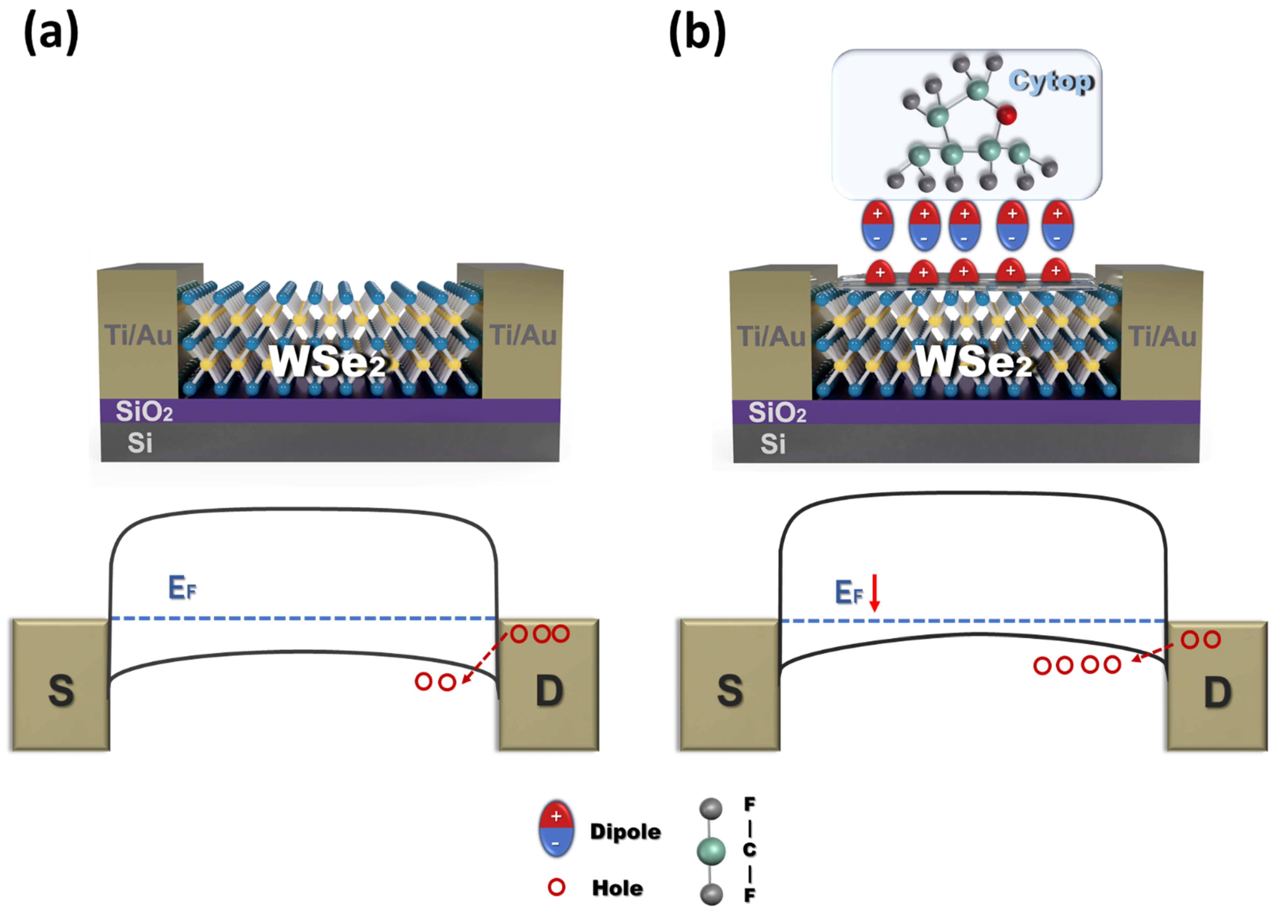
Figure 7.
Stability test of F-WSe2. (a) Reduction in bias stress due to passivation effect due to Cytop doping. (b) F-WSe2 (TA = 200 °C) transfer characteristics of the device with increasing time stored in air at room temperature. All electrical characteristics were measured in air. (c) Threshold voltage and (d) hole mobility change of F-WSe2 device annealed at TA = 200 °C after Cytop doping for 25 d in air.

Publisher’s Note: MDPI stays neutral with regard to jurisdictional claims in published maps and institutional affiliations. |
© 2021 by the authors. Licensee MDPI, Basel, Switzerland. This article is an open access article distributed under the terms and conditions of the Creative Commons Attribution (CC BY) license (http://creativecommons.org/licenses/by/4.0/).
Share and Cite
MDPI and ACS Style
Lee, H.; Hong, S.; Yoo, H. Interfacial Doping Effects in Fluoropolymer-Tungsten Diselenide Composites Providing High-Performance P-Type Transistors. Polymers 2021, 13, 1087. https://doi.org/10.3390/polym13071087
AMA Style
Lee H, Hong S, Yoo H. Interfacial Doping Effects in Fluoropolymer-Tungsten Diselenide Composites Providing High-Performance P-Type Transistors. Polymers. 2021; 13(7):1087. https://doi.org/10.3390/polym13071087
Chicago/Turabian StyleLee, Hyeonji, Seongin Hong, and Hocheon Yoo. 2021. "Interfacial Doping Effects in Fluoropolymer-Tungsten Diselenide Composites Providing High-Performance P-Type Transistors" Polymers 13, no. 7: 1087. https://doi.org/10.3390/polym13071087
Note that from the first issue of 2016, this journal uses article numbers instead of page numbers. See further details here.