Microwave Liquid Crystal Technology


Institute for Microwave Engineering and Photonics, Technische Universität Darmstadt, 64283 Darmstadt, Germany
*
Author to whom correspondence should be addressed.
†
These authors contributed equally to this work.
Crystals 2018, 8(9), 355; https://doi.org/10.3390/cryst8090355
Submission received: 2 August 2018
/
Revised: 24 August 2018
/
Accepted: 28 August 2018
/
Published: 5 September 2018
(This article belongs to the Section Liquid Crystals)
Abstract
:Tunable Liquid Crystal (LC)-based microwave components are of increasing interest in academia and industry. Based on these components, numerous applications can be targeted such as tunable microwave filters and beam-steering antenna systems. With the commercialization of first LC-steered antennas for Ku-band e.g., by Kymeta and Alcan Systems, LC-based microwave components left early research stages behind. With the introduction of terrestrial 5G communications systems, moving to millimeter-wave communication, these systems can benefit from the unique properties of LC in terms of material quality. In this paper, we show recent developments in millimeter wave phase shifters for antenna arrays. The limits of classical high-performance metallic rectangular waveguides are clearly identified. A new implementation with dielectric waveguides is presented and compared to classic approaches.
1. Introduction
Liquid Crystal (LC) technology paved the way for today’s communication and information industry. It found wide application in display technology and enabled modern devices for mobile computing such as smartphones, being present everywhere. Most of these devices (except for OLED) are based on the birefringence properties of LC. In the optical domain LC is packed between two polarization grids and is used to adaptively turn the polarization angle of light transmitted perpendicular to the LC’s surface. This twisted nematic (TN) cell is the foundation principle for all modern liquid crystal displays (LCD). This principle has been developed in Switzerland and the US beginning in the 1960s and patented early 1970s [1,2], respectively. Figure 1 shows the fundamentals of most of today’s LCDs.
Birefringence is a material property which is known in microwave engineering as anisotropy represented by the permittivity tensor
within the material’s coordinate system (). The main differences compared to optical applications are founded in the much larger wavelength (up to several instead of less than ). The rotation of the polarization angle is a niche application at microwaves. There, the anisotropy is usually adopted in order to present a variable effective permittivity to the electromagnetic wave. In addition, specific electromagnetic design rules must be fulfilled. Especially impedance matching is critical for the device’s dimensions. In the following section, the microwave liquid crystal technology is described starting from fundamental device concepts, to material properties and characterization. After the introduction of a use case, high-performance LC-based phase shifters for antenna systems are presented for 100 GHz communication systems. Millimeter wave and submillimeter wave communication systems are a very hot topic in nowadays research. As we will see, high-performance liquid crystal devices can play a crucial role.
2. How to Use LC at Microwave Frequencies?
The mixtures used for microwave applications are thermotropic calamitic nematic LCs. The phase transitions occur at certain temperatures, where the liquid crystalline mesophase is defined thermodynamically stable between the melting point of the crystalline phase and the clearing point to the isotropic liquid phase. In this mesophase, liquid crystals show an orientational order but lack translational periodicity. In comparison to the smectic phase, the elongated molecules tend to align parallel to each other but are not organized into layers. The fundamental properties of nematic LCs versus temperature are shown in Figure 2. LC exhibits an anisotropy in the crystalline as well as in the nematic phase, whereas only the nematic phase can be used for electrically tunable RF circuits/devices.
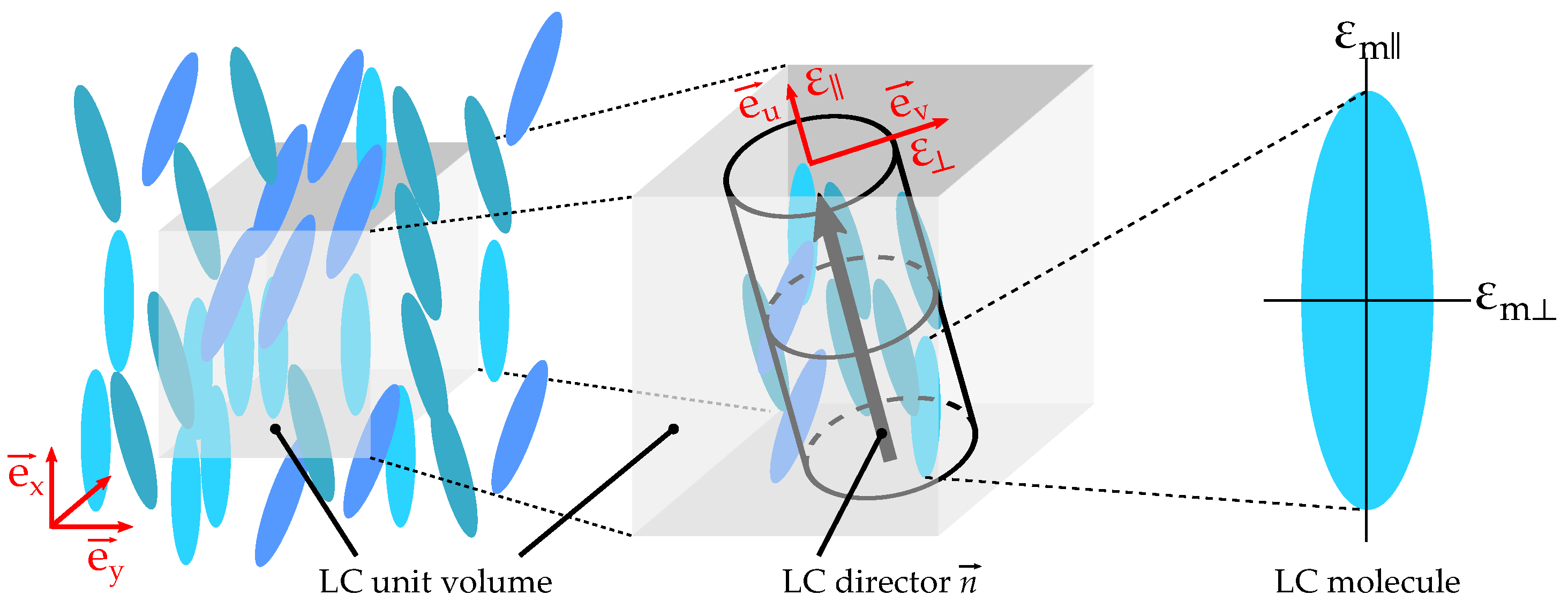
The molecules can be depicted with a rod-like shape where their uniaxial anisotropy is used to realize tunable devices. Due to the molecule’s rotational symmetry, the permittivity tensor Equation (1) reduces to
with the ()-coordinate system aligned with the director of the LC volume, according to Figure 3. The director is a macroscopic unit vector giving the main direction of the molecules inside a unit volume element. The values of the permittivities and , and therefore, the LC’s anisotropy n
are material and temperature dependent, refer to Section 3.
The electric displacement field interacts with an electric field according to
As displacement and electric fields on one side and the permittivity tensor on the other side are defined in different coordinate systems, effective displacement must consider the rotation of the coordinate systems by introducing the rotation matrix .
The degree of freedom to realize tunable devices is now this rotation matrix , leading to a tunable effective permittivity
with the tilt angle between both coordinate systems. For example, when , a continuously tunable effective permittivity can be achieved as
This example can be visualized with a simple parallel-plate capacitor. The LC material is sandwiched between two electrodes and an electric field is applied as shown in Figure 4.
The LC material in tunable devices is described by the continuum theory [3]. The system’s energy is defined based on the Gibbs Free Energy, which is affected from the elastic deformations, external electric and magnetic fields as well as anchoring effects. Thus, an increase in the Gibbs Free Energy is minimized by changing the orientation of the director to reach equilibrium.
From this, three different methods can be derived for the practical implementation of alignment of LCs.
In the presence of an external electric field, the energy
is causing a re-orientation of the director to achieve minimum system energy, if a certain threshold energy is overcome. It should be noted that is positive for millimeter wave optimized nematic LCs. Therefore, the director tends to align in a way that is parallel to the electric field lines.
In principle, the same is valid for magnetic fields, where energy is defined as
At last, surface forces (which have been neglected in Figure 4) can also be used to align LC molecules. Any physical impurities on the boundaries of the cavity result in interaction between the boundary and the LC molecules. According to the Rapini–Papoular model [4,5,6], this interaction energy density is given as
with the director and the preferred alignment for the polar and azimuthal angles specified by (, ) and (, ). The energy depends on the anchoring strength and , which are LC material and anchoring surface-dependent parameters.
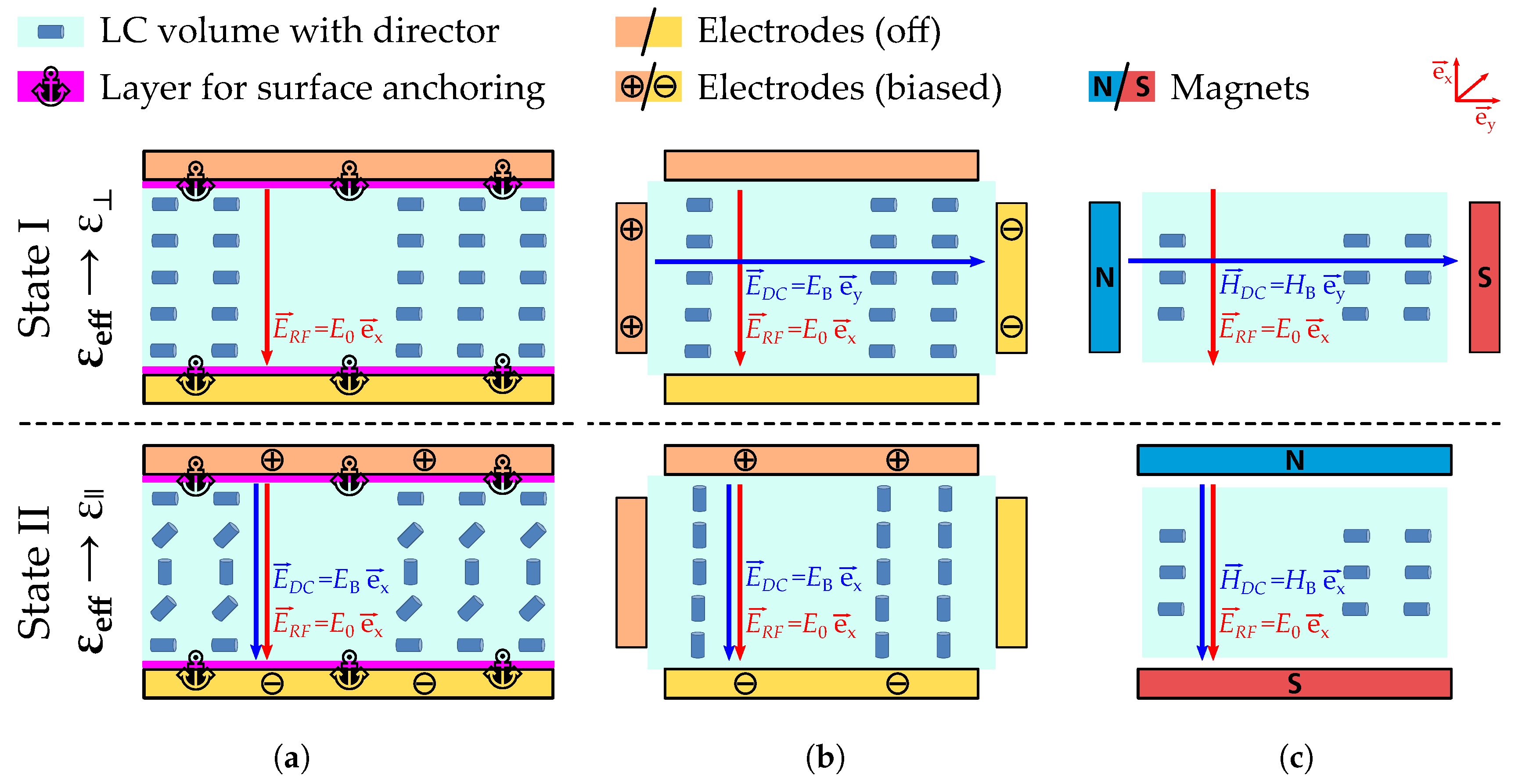
In practical applications, different orientation mechanisms are combined according to Table 1. For example, the combination of surface anchoring and electrical biasing concepts as it is used in the LCD technology, compare Figure 5a. Without the electric field, the directors are aligned in state I and with applied field they change their orientation towards state II, at which the numbering of the states has been arbitrarily chosen. This mechanism is preferred in planar devices. One reason for the limitation to planar devices is that the forces of the surface anchoring are weak compared to electric forces. Hence, the tuning speed from on- to off-state, which are dependent on the sheet thickness, are much lower than those from off- to on-state.
For volumetric waveguide-based components, solely electrical biasing concepts (compare Figure 5b) are preferred, e.g., by applying two electrodes in perpendicular spacial directions. By switching on one pair of electrodes, the directors are aligned for state I. By toggling the other pair of electrodes, the directors will orient into state II. By proper superposition of both fields, any alignment between these two states can be reached as well. It is also possible to rotate a pair of magnets around the structure to realize a variable alignment, compare Figure 5c. Obviously, this approach is not smart in terms of space requirements and power consumption. Hence, this method is only applied for material characterization and for a first proof-of-concept in the lab, see Section 3.
At this point, it is clear how the alignment of the director can be technically realized. For application in tunable components, the RF signal and the control (bias) must be discriminated. For magnetic alignment, the bias field and the RF signal’s E-field are decorrelated by definition. This is different for both other cases, where the electric field is used to reach at least one state. The only difference in RF signal and bias E-field is the frequency. The minimization of overall system’s energy according to Equation (8) must hold also in this case. The temporal behavior of the LC volume is encapsulated in the elastic term as this includes the mechanical materials properties. Due to the viscosity, the director cannot follow an electric field with fast changing amplitude. Additionally, the dielectric contrast required for LC steering is much higher at DC than at RF frequencies. Hence, the influence of the RF field can be neglected. This is also relevant for the linearity of the components. The electric tuning of the material leads automatically to a non-linear behavior of the components, as the RF field will also change the state of LC. There are just few measurements of LC’s linearity published. In 2006, IP3 measurements of two different nematic liquid crystals have been published in [7]. Measurements of a phase shifter showed that the IP3 of this device is in the range of 60 dBm. Since then, no other measurements have been published. The excellent large signal characteristics obtained in this measurement already fulfill the requirements of many RF applications. Furthermore, the achieved performance makes linearity measurements of LC very difficult, as standard measurement equipment is at its boundaries. Hence principles for measuring passive intermodulation (PIM) must be adapted for LC non-linear characterizations. This specific topic will gain more interest in future as commercialization advances. Up to now, no devices showed significant non-linearity.
After the fundamental device concepts have been discussed, the material must be characterized before we will show implementation advances around 100 GHz. For material characterization different realizations have been discussed recently. In the following we will show the most important ones.
3. Material Properties and Characterization
The state-of-the-art setup for LC characterization at 19 GHz and 30 GHz is a precise resonator-based setup, making use of the cavity perturbation technique. In [8] the resonator based dual mode characterization technique was introduced, where a resonator is measured with and without LC inside a sample holder made of silica, see Figure 6a. Due to the dielectric properties of LC, the field distribution, and therefore, the resonance frequency of the excited mode will shift compared to the reference measurement. By this, the permittivity as well as the loss tangent of the material can be determined. Although this kind of measurement is limited to one single frequency, the dielectric properties of the LC can be determined much more precisely than with broadband measurement setups. A detailed mathematical description of this method can be found in [8].
By using a dual-mode cylindrical resonator, the permittivity and dielectric loss of LC can be measured for both parallel and perpendicular orientation in one single step, see Figure 6b. For this, two perpendicularly aligned modes are excited. The terms “parallel” and “perpendicular” define the two extreme cases of orientations of the LC molecules, where the long axes of the molecules are aligned parallel or perpendicular with respect to the applied RF field, respectively. The silica tube is placed in the center of the resonator to ensure maximum field interaction, and therefore, high sensitivity. The resonator is excited by rectangular waveguides being weakly coupled to the resonator by means of a small coupling iris, see Figure 6c. During the characterization, the LC’s long axes are aligned parallel to the silica tube with the help of permanent magnets.
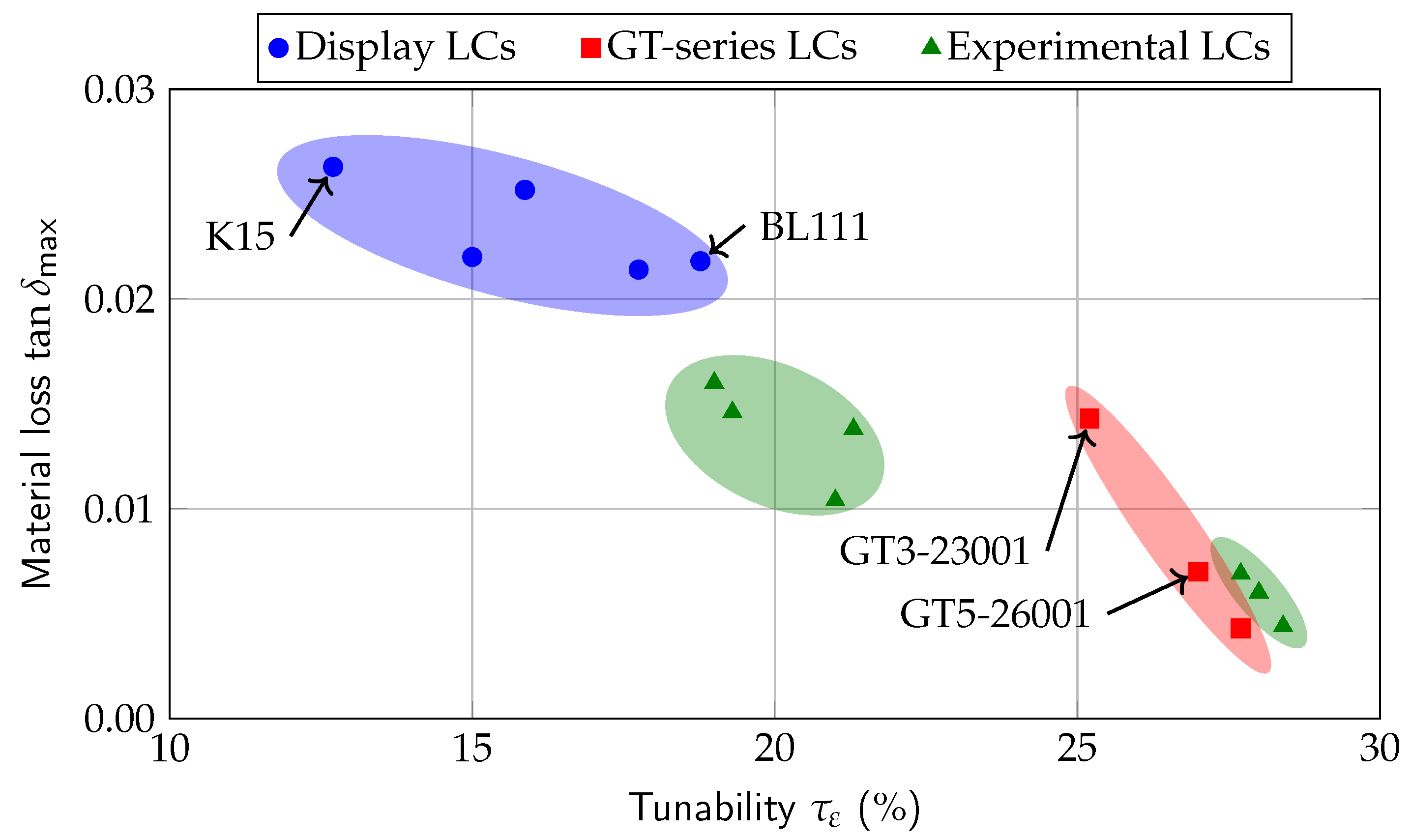
With this characterization method, the LC mixtures could be improved in terms of loss tangent as well as relative material tunability
as can be seen in Figure 7. The first tunable microwave devices in the early 2000’s were realized by using display LCs such as K15 or BL111. A bit later, new mixtures were specifically synthesized for the microwave range. The LC mixture being used for the components presented in this paper is the mixture GT5-26001 from Merck KGaA, Darmstadt, Germany with a permittivity between and dielectric losses of . A comparison of different LC mixtures is summarized in Table 2. A review on recent material development can be found in [9].
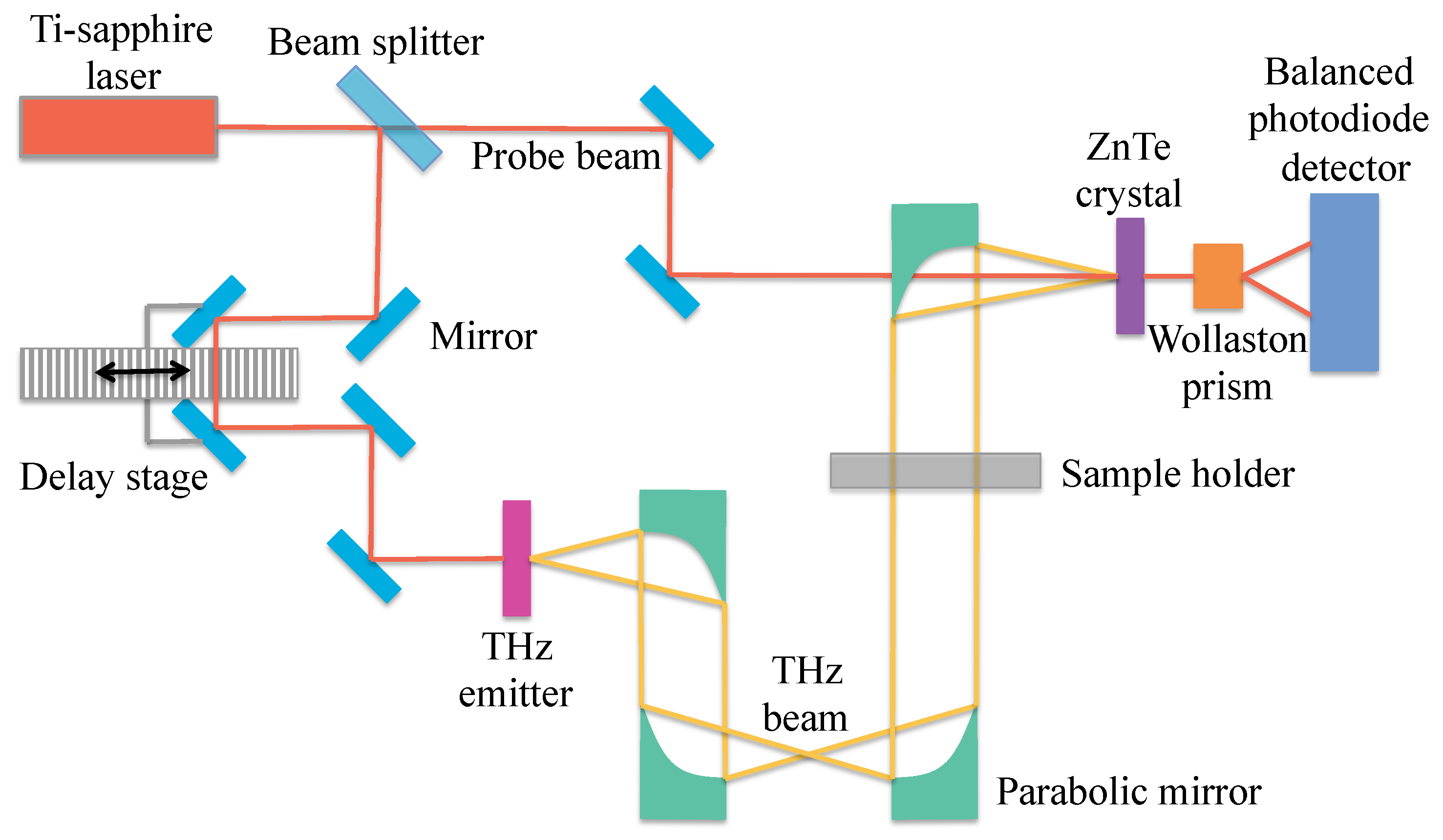
One advantage of LC compared to other technologies such as semiconductors is a decreasing dielectric loss with increasing frequency in the range above 15 GHz. Measurements up to THz have been conducted, using a time-domain spectroscopy (TDS) THz measurement system as shown in Figure 8.
The beam generated by a Ti-sapphire laser is split up in the beginning. While one part of the beam is used as probe beam, the other one is passing a delay station before hitting the THz emitter, e.g., a biased GaAs-based photoconductive emitter. The THz beam is guided via parabolic mirrors through the sample holder and afterwards to the ZnTe crystal for THz detection. The THz as well as the probe beams are propagating collinearly through the crystal. There, the THz beam induces a birefringence, which can be read out by the linearly polarized probe beam. By this, the linear polarization is rotated by the THz beam. Together with a -wave plate, a beam splitting polarizer and a set of balanced photodiodes, the THz beam’s amplitude can be mapped by monitoring the rotation of the probe beam’s polarization at a variety of delay times. Therefore, the LC properties can be determined by a differential measurement method, comparable to the resonator-based characterization. Moreover, it is a highly interesting feature of THz TDS, to be able to get full information of the electric field, i.e., amplitude and delay.
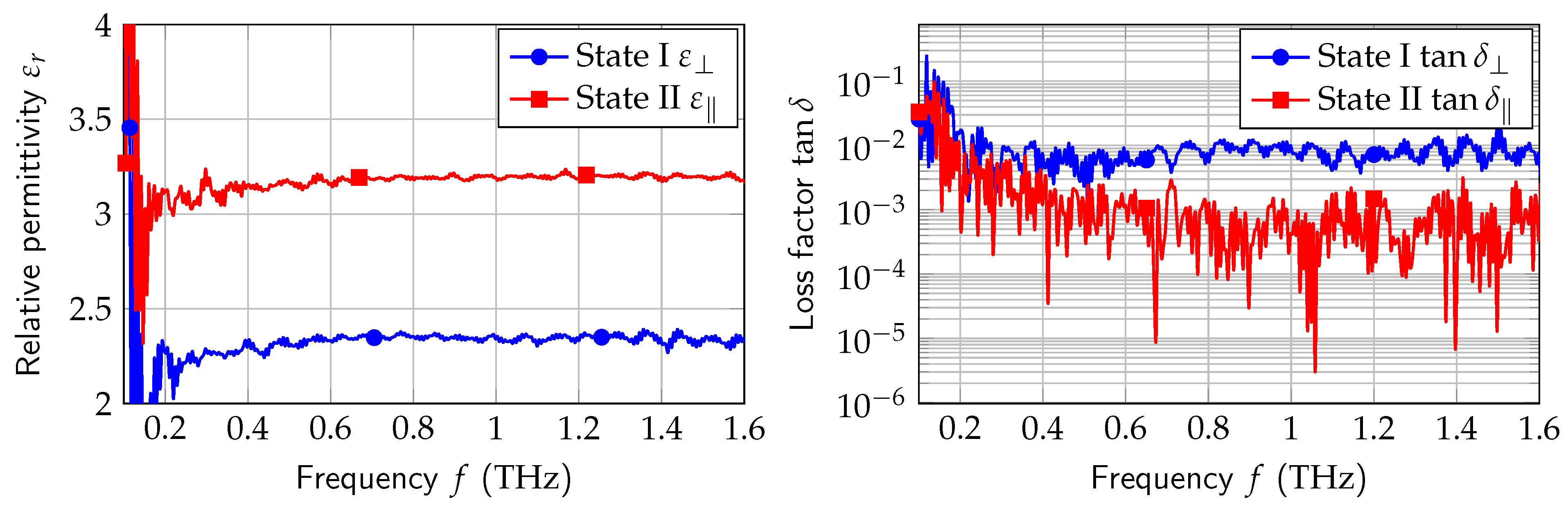
One of the characterized LCs was the mixture GT3-23001, which shows an almost constant permittivity over a wide frequency range between 200 GHz to 1.5 THz, see Figure 9. The permittivities of and fit well (5.1% deviation for the perpendicular state and % for the parallel state) with the values measured with the previously mentioned resonator setup at 19 GHz. The dielectric losses are in the expected order of magnitude, but could not be determined precisely, due to the low dynamic range of the TDS system. Further information and a more detailed description can be found in [11].
Therefore, LC has been proven as well suitable material for the realization of continuously tunable components not only in the microwave- but also in the (sub-)millimeter wave and THz range.
4. Use Cases for LC-based Microwave Devices
Modern communication systems are on the way to the 5th generation (5G). The paradigm change includes three different main directions including increased data rate up to several gigabit per second, low-latency communication down to milliseconds, and finally, increased user density [12,13,14,15]. While most of the functionality will be covered by improved network architecture including e.g., network slicing, there are new systems to be deployed at higher frequencies. As the ITU plans to standardize a new 60 GHz band at WRC’19, first providers demonstrated the potential at international sport events such as the last winter Olympiad in South Korea [16,17]. Millimeter-wave (mmWave) communication at 60 GHz and higher frequencies is mainly limited by high free-space path loss and atmospheric impairments, compare Figure 10.
A second trend in mobile communications is characterized by worldwide ubiquitous communication envisioned for a long time but brought to the real world by projects like Google’s LOOM and OneWeb. These concepts summarized in the New Space Initiative use flying platforms such as balloons or low earth orbit (LEO) satellites to provide communication services. Independently from the final system concepts, high-gain antennas are required to establish a stable communication link from users’ terminals to the network. For systems operated at Ka (26.5–40) or Ku (12–18) bands, high-gain antennas are required to bridge large distances between terminals, e.g., 600 to the LEO satellite, which corresponds to approximately 180 dB of path loss at Ka-band. For a 60 GHz system this free space path loss is already reached at a distance of 400 km. In practice, the reach is much lower due to mentioned atmospheric impairments such as absorption by oxygen () and rain attenuation ( for medium rain) for 60 transmission, according to ITU recommendations for standard atmosphere [18,19].
As the transmitter output power is limited, the path loss must be compensated by the gain of the antenna. The gain g of an antenna and the beam width are connected by
with the antenna’s efficiency and the half-power beam width and in azimuth and elevation, respectively. Hence, to realize an antenna with enough gain (), the width of the beam gets with values of less than very narrow. If you now want to establish a connection, the antennas must be aligned in a precise way.
For the alignment of antennas, different methods can be used. Among the very common ones are mechanically steered antennas, where the antenna’s axes are motorized. This results in heavy systems which additionally require high maintenance efforts. Beside this, electronically steerable antennas have been developed and explored in the last centuries. These are based on the array concept where many antenna elements are combined with respect to phase and amplitude to synthesize a steered antenna beam pattern. For high-frequency high-bandwidth applications as indicated by previous scenarios, analog beam-steering concepts are a low-cost alternative to fully digital systems. Figure 11 gives an overview on the most important implementations.
LCs are the most promising candidates for applications above 15 GHz as their dielectric loss is superior compared to other technologies such as ferroelectrics [20,21,22,23,24,25] and ferrites [26,27,28]. A direct competitor are micro-electro-mechanical systems (MEMS) [29,30], which utilize mechanical changes on the micro scale to implement phase shifter components required for array antennas. Researchers around the world develop new materials which can be used for tunable devices. Recent examples are e.g., phase change materials [31,32] and electrochromic materials [33]. These have a great potential, and should be monitored consciously.
To describe the requirements and properties of LC-based array antennas in more detail, the use case of a Ka-band LEO satellite system is discussed. As the satellite is non-stationary, the antennas must track the satellite all time. The orbit time of such a satellite is around 120 , so the phase shifters have to provide tuning speed of more than roughly 70/min [34]. Hence, realization technology and material properties must match the requirements. The change in electrical length of the phase shifter is proportional to the dielectric contrast (anisotropy) of the used LC mixture. The phase shift of a transmission line phase shifter is defined by
with the physical line length l. The differential phase shift is defined as
Hence, LC mixtures with high anisotropy, low dielectric loss but also high viscosity are targeted. Beside the material properties, the technological implementation is also challenging, as a hermetic liquid-proof must be realized to prevent the LC from leaking. One example for the realization of fully integrated planar LC-based array antennas has been published in [35]. Here, the phase shifters are implemented as meandered microstrip line phase shifters directly coupled to an array of patch antennas, see Figure 12. While planar implementations are well suited at the lower end of the frequency band, ohmic losses of the microstrip line topology increase with frequency. While the planar topology is meanwhile followed by the company Alcan Systems Darmstadt, Germany, research is focusing on other implementations such as high-performance rectangular waveguide based implementations. To compare different implementations the phase shifter Figure of Merit (FoM) is defined as
which is the ratio of the maximally achievable phase shift divided by the highest insertion loss for all tuning states max IL.
5. Metallic Rectangular Waveguides
A very common approach at Ka-band frequencies around 30 GHz for the realization of tunable LC-based high-performance RF components is the dielectrically filled metallic waveguide. The dielectric filling contains a cavity, in which the tunable LC material is filled. Hence, the cross section of the rectangular waveguide is (partially) filled with tunable LC, see Figure 13.
By controlling its effective permittivity, the electrical length of the waveguide can be varied, resulting in a tunable delay line. In combination with the intrinsic low ohmic loss of the waveguide, this leads to an easy realization of phase shifters with a high figure-of-merit (FoM) of more than 120/dB [36]. The LC orientation is controlled by means of six pairs of electrodes, which need to be included into the waveguide, due to its electrical boundaries. A high complexity of these biasing electrodes is required for avoiding the propagation of parasitic stripline modes between the electrodes and the waveguide’s walls. An example for the parasitic modes as well as the biasing electrodes’ complexity is given in Figure 14. The electrodes were processed on a thin Hostaphan film of 50 thickness, being lead to the outside of the metallic waveguide for contacting to the voltage supply.
Such phase shifters are used in lightweight horn antenna arrays for satellite communications. Although the LC’s response time is comparatively high, it is already enough for specific applications, such as the tracking of a low earth orbit (LEO) satellite from a geostationary (GEO) satellite, where a steering speed of maximum 73/min is required [11,34,37].
The concept of a dielectrically filled rectangular waveguide can also be adapted to W-band frequencies around 100 GHz [38,39]. There, the waveguide was realized in split-block technology made of brass, where the bottom part has a u-shape, being sealed with a top lid, see Figure 15. The waveguide is tapered in width and height within the dielectrically filled section to still provide a single mode propagation. The tapering is done by means of transformer steps. The dielectric cavity is made of PTFE ( and [40]), being tapered in a triangular shape. The PTFE cavity is also designed in a u-shape, which is sealed by pressing the metallic lid on top.
After sealing, the LC is filled into the dielectric cavity through filling holes on the top part of the split-block, see Figure 16. With the help of a syringe the LC is flushed through the cavity, by which the amount of air bubbles within the RF path can be significantly reduced. The LC section within the dielectric cavity has a width of a height of and a length of , providing a differential phase shift of more than 360 according to the simulation carried out with CST Studio Suite. This demonstrator can only be biased magnetically, since no biasing electrodes can be included to this design. Hence, rare-earth magnets were placed outside the split-block during the measurements, see Figure 16. They are generating a magnetic field of around . The measurements were carried out using an Aritsu 37397C vector network analyzer (VNA) combined with two 3740A-EW extensions for frequencies in the extended W-band. These first proof-of-concept measurements revealed a good matching of −10 dB over an 8 bandwidth. This limitation in bandwidth is due to the narrow-banded quarter-wave transformer steps. A differential phase shift between 300 to 330 was achieved, being 60 to 100 less than simulated. This is due to the flexible PTFE material which makes an exact processing of the LC cavity difficult. Further, the press-fit sealing causes a narrowing of the LC section. Accompanied with an insertion loss of less than 3 , this results in a phase shifter FoM between 105/dB to 148/dB from 90–107, as can be seen from Figure 17. The deviation of the insertion loss has its origin in the interruption of the current walls, due to a non-perfectly closed split-block.
However, it is very challenging to implement an electrical biasing system due to the limited space as well as the electrical boundary conditions. Within the limited space of 1.6 mm in width for the dielectrically filled section, several pairs of electrodes need to be placed on the substrate material, including stepped impedance structures for stripline mode suppression.
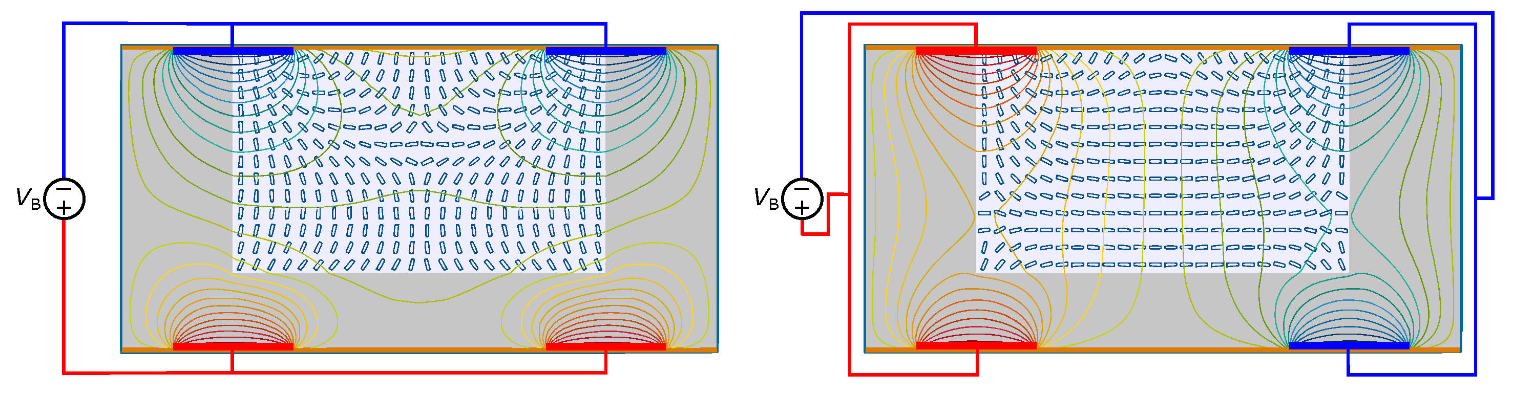
Simulations with the in-house director dynamics simulation tool SimLCwg [8] proved, that two pairs of electrodes are sufficient but not ideal for a proper LC alignment, as shown in Figure 18 [41]. There it can be seen, that a small region with a perpendicular LC alignment will still be left in the center of the waveguide when the LC is supposed to be aligned parallel. However, an odd number of pairs of electrodes is not possible, since the centered filling system of the split-block in combination with the press-fit sealed PTFE container should be kept in the design. Also, the limited space in combination with lithography challenges are limiting the realization of more than three pairs of electrodes.
The substrate material on which the electrodes were processed had to be as thin as possible. By this, the impedance of the parasitic microstrip line consisting of the biasing electrodes and the waveguide walls is decreased. Hence, the excitation of the unintended stripline modes is suppressed. For a first proof, a 20 thin PET film was used. As metallization, chromium was evaporated on the PET film. After this, the electrodes including their stepped impedance structures are processed on the substrate by means of lithography steps. Further, the split-block design was changed in the way that the electrodes can be guided to the outside. There, the voltage source can be connected to the biasing lines with the help of spring-probe-pins. The design of the PTFE container was changed as well. Due to the mounting of the electrodes, the taper was chosen as discrete taper instead of a triangular taper. The processed biasing electrodes, the re-designed split-block as well as PTFE container are given in Figure 19.
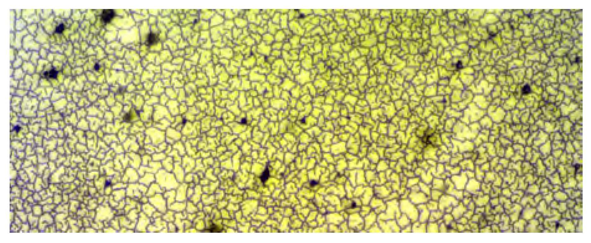
However, it was not possible to characterize the electrically biased phase shifter, since the electrodes did not work properly. A microscopical investigation of the electrodes revealed cracks within the metallization as well as the substrate material itself, as can be seen in Figure 20. These cracks are originating both from the expansion during the evaporation process as well as the lithography treatments, e.g., etching. The high chromium vacuum melting temperature of 1920 caused an expansion of the substrate as well as a shrinking while cooling after the evaporation. Hence, microscopic cracks are occurring and no continuous electrical contact could be provided all over the biasing lines. Additionally, the thin PET substrate cannot withstand the contacting of the spring-probe-pins, which are damaging the substrate irreversibly.
At least the simulations can give an insight into the possible functionality of the electrically biased LC metallic waveguide phase shifter in split-block technology, see Figure 21. The matching could be improved compared with the simulation results of the magnetically biased phase shifter in Figure 17. However, the insertion loss is increased by 1 dB due to the biasing system, resulting in a phase shifter FoM of around 115/dB. This still includes the ideal LC alignment assumed by CST Studio Suite. In a real measurement, the alignment would not be ideal anymore and the phase shift, and therefore, the phase shifter FoM would degrade.
Hence, it is obvious that the realization of a metallic waveguide based W-band LC phase shifter is challenging. Further, the integration of a biasing system into the dielectrically filled waveguide is always introducing additional loss. Thus, a new technology needed to be found to easily overcome all these challenges. This technology was found in the realization of tunable dielectric waveguides based on LC, being discussed in the following.
Not only that the realization of the biasing electrodes is very challenging and their integration into metallic waveguides introduces additional losses, but also RF leakage due to unintended slits in the split-block design is playing a dominant role. If the metallic interconnections are not perfectly sealed in the areas where the wall currents are flowing perpendicularly to these slits, RF leakage occurs. This effect as well as the additional losses from the integrated biasing electrodes play an increasing, non-negligible role with increasing frequency. Further, the higher the frequency, the higher the impact of the skin depth loss of metallic components.
6. Dielectric Waveguides
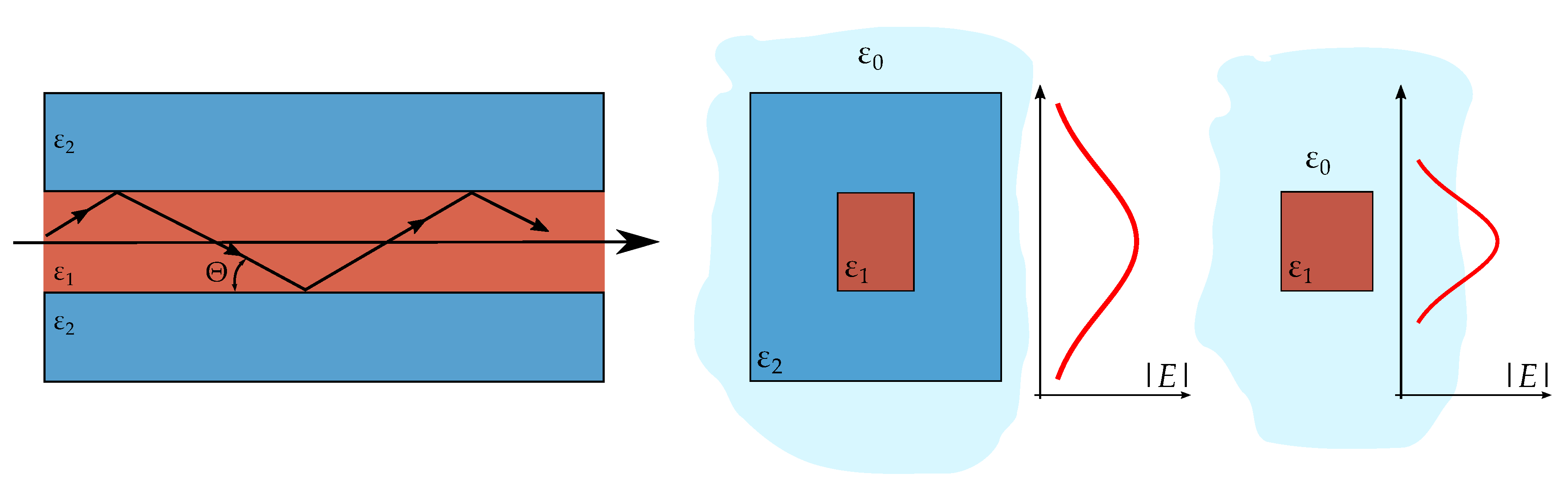
Dielectric waveguides are predestinated to overcome aforementioned drawbacks of metallic rectangular waveguides. They offer a low-cost fabrication and low-loss propagation. For example, 3D-printing or injection molding fabrication can be used, and no metallic component is required for the waveguide itself. In addition, the design of LC-based dielectric waveguides is comparatively simple. Due to their electrically unshielded design, electrodes can be placed around the dielectric waveguide without disturbing the propagating wave. Their guiding characteristic can be approximated by the geometrics approach, see Figure 22. Assuming a dielectric slab with a core material, surrounded by a cladding material , with . Internal reflections at the boundary layer of core and cladding occur according to Snell’s law if the angle is below the critical angle
With the internal reflections, the propagating wave is confined in the dielectric core. Two types of dielectric waveguides are the most prominent ones, the step-index fiber and subwavelength fiber, see Figure 22.
Whereas the subwavelength fiber consists of only one single dielectric material, the step-index fiber comprises of two dielectrics. In both cases, evanescent fields are propagating outside the dielectric core. Since the subwavelength fiber only consists of one single dielectric core, the evanescent field propagates outside the waveguide in air, which leads to a low-loss propagating. On the other hand, these fields are sensitive to discontinuities or external influences, such as metallic structures. Using a cladding as for the step-index fiber, all evanescent fields are already decaying inside the dielectric waveguide. These two characteristics are very important for LC-based tunable dielectric waveguides, which will be discussed in the following.
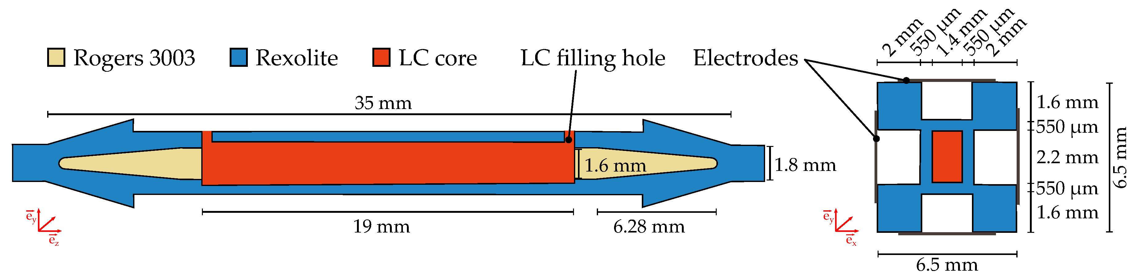
The design of a tunable step-index fiber designed for W-band frequencies which has been recently published in [42] is shown in Figure 23.
The presented design uses Rogers 3003 as non-tunable core material with a permittivity of and dissipation factor of . As cladding material Rexolite 1422 from C-Lec Plastics Inc., Philadelphia, PA, USA is used, with and . To achieve tunability, LC is used as core material instead of Rogers 3003. The core is untunable and still manufactured from Rogers 3003, see Figure 23. The phase constant of the propagating wave can now be adjusted by means of the LCs permittivity. As the perpendicular permittivity is below the permittivity of the surrounding cladding, RF leakage would occur, as the propagation condition is not fulfilled anymore. To prevent RF leakage, air gaps are included in the cladding to reduce its effective permittivity. With this design step, the propagation condition is still fulfilled, even for the lowest LC permittivity, and the evanescent fields are still decaying inside the effective cladding. The main advantage of the step-index fiber is that electrodes can be directly attached on the cladding. Therefore, the design of the biasing electrodes can be kept very simple. For characterization purposes, transitions were designed to provide a smooth mode conversion from the fundamental mode of the rectangular metallic waveguide to the mode of the dielectric waveguide and vice versa [42,43]. Several tapers, such as for the cladding and core are used to achieve mode matching and for keeping losses due to radiation on a low level.
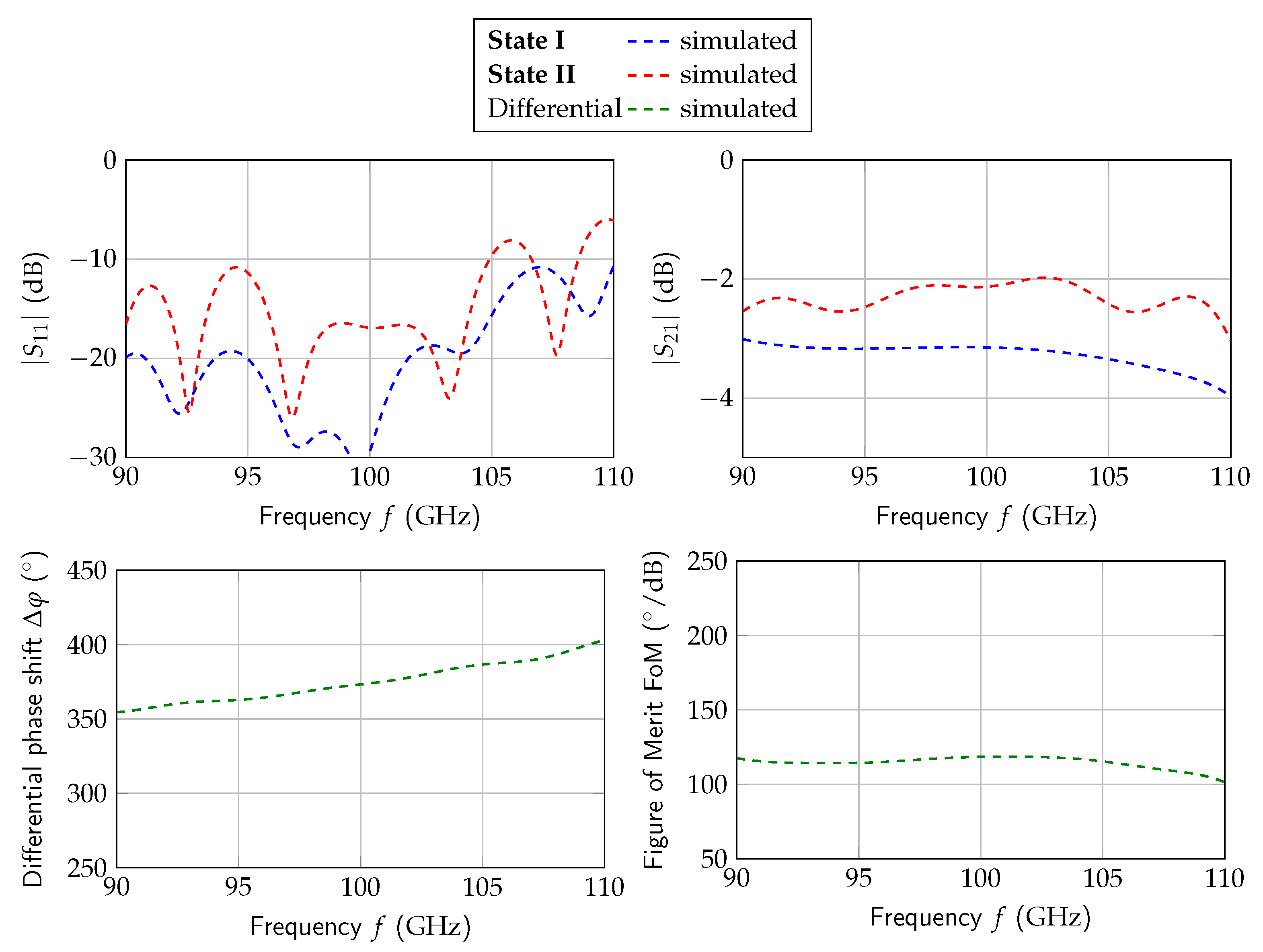
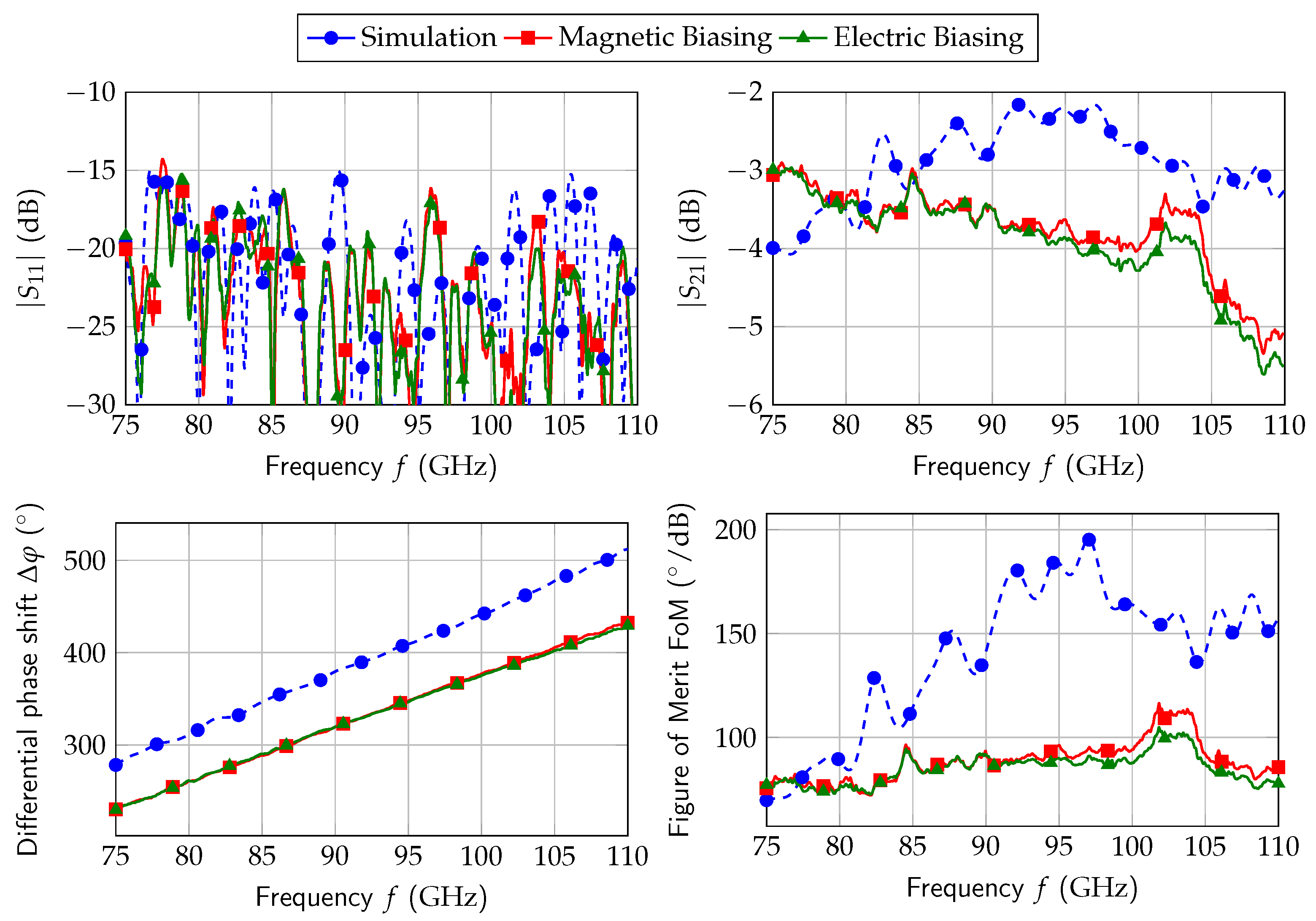
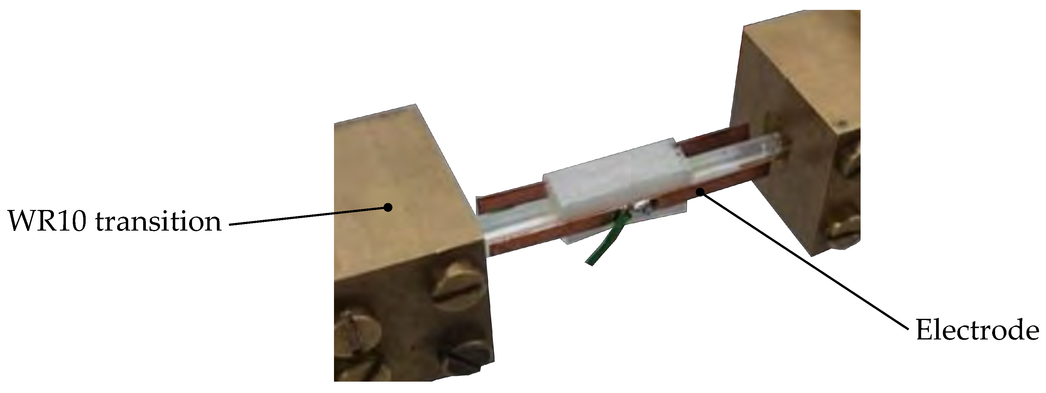
The measurement setup is depicted in Figure 24. It consists of the fabricated dielectric phase shifter including two WR10-to-subwavelength fiber transitions for connection to a VNA. The phase shifter was fabricated in two parts milled out of Rexolite, being glued together by using an UV glue. By this, LC leakage can be easily avoided and two filling holes are left for later LC filling. To show the simplicity of the biasing system, adhesive copper tape was used, being directly stuck on the cladding. Furthermore, a voltage of was applied to the parallel plate biasing configurations. The achieved S-parameters as well as the phase shift and FoM are given in Figure 25. It can be observed that the phase shifter is well matched with over the whole frequency range. The insertion loss is in a range of 3 to 5 . In comparison to the simulation, a deviation can be observed. The reason was found in the splice, which was not included in the simulation. Further, the dielectric loss of the glue itself was unknown at the time of the simulation, but it is expected to be higher than that of Rexolite. Nevertheless, with the LC GT5-26001 an FoM of around 90/dB was achieved between 94–105, accompanied with a differential phase shift of 220 to 420, see Figure 25. It is noticeable, that the simulated phase shift was not achieved in the measurement. This is due to fabrication tolerances in the milling process. With a precision of 30 , the fabricated LC cavity is slightly reduced, resulting in a reduced phase shift. Furthermore, the glue used in the assembling can flow into the cavity and can further decrease the LC volume. In addition, the LC might not be perfectly aligned. However, both insertion loss and phase shift show the same behavior independence of the biasing concept. This is an outstanding result for tunable devices based on LC, especially for in comparison to metallic waveguides. Here, electrical biasing systems always introduce additional losses and could not align the LC as properly than for the magnetic biasing.
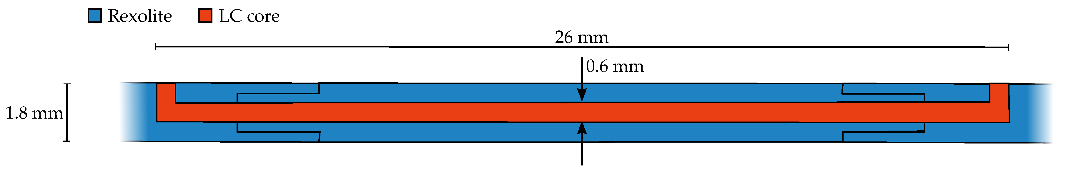
With the design of the step-index fiber, a high-performance but bulky phase shifter was presented, which also allows a feasible phase shifter design for terahertz frequencies. However, for the integration of a dielectric waveguide phase shifter, e.g., in phased arrays, a more compact design is needed. As shown in Figure 26, a subwavelength fiber is well suited for such an application, due to its smaller dimensions. In [43] a phase shifter design was presented.
The cross-section of the presented phase shifter is depicted in Figure 26. The main part consists of a quadratic Rexolite fiber with an edge length of . For tunability, a circular LC core is included. Like the step-index design, metal plates were used for the electric biasing, being placed in a large enough distance to the fiber, to not disturb the evanescent fields. The measurement setup, including the electric biasing system is shown in Figure 27. With a distance of the electrodes of 3 from the edge of the Rexolite body, the metallic plates are not disturbing the propagating wave. To ensure a proper position, Rohacell 31HF, from Evonik Industries, Darmstadt, Germany is a special high performance foam suitable for high frequency applications. Its permittivity is around 1.05 with a dissipation factor of 0.01 at 27 GHz. As LC, GT5-26001 was used. For characterization, the same WR10-to-subwavelength fiber transition were used as introduced before. The measured S-parameters are shown in Figure 28. It can be noticed, that the phase shifter is well matched over the whole W-band.
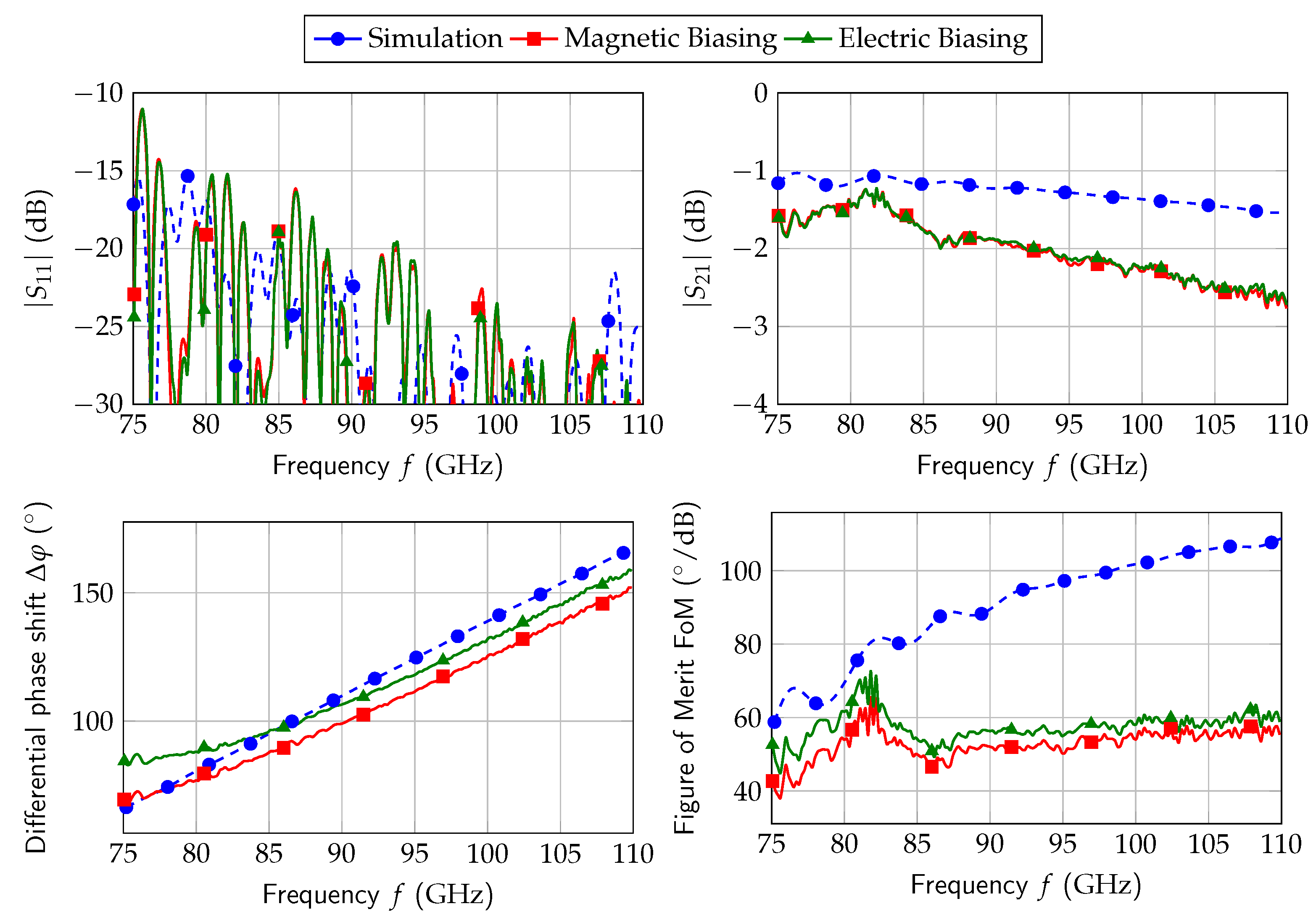
The achieved FoM is in a range of 60/dB, as the phase shifter reaches a differential phase shift between 90 to 160 accompanied with an insertion loss of 1.5 dB to 2.9 dB. Again, the results for magnetic and electric biasing are in a good agreement which again highlights the advantage of this technology.
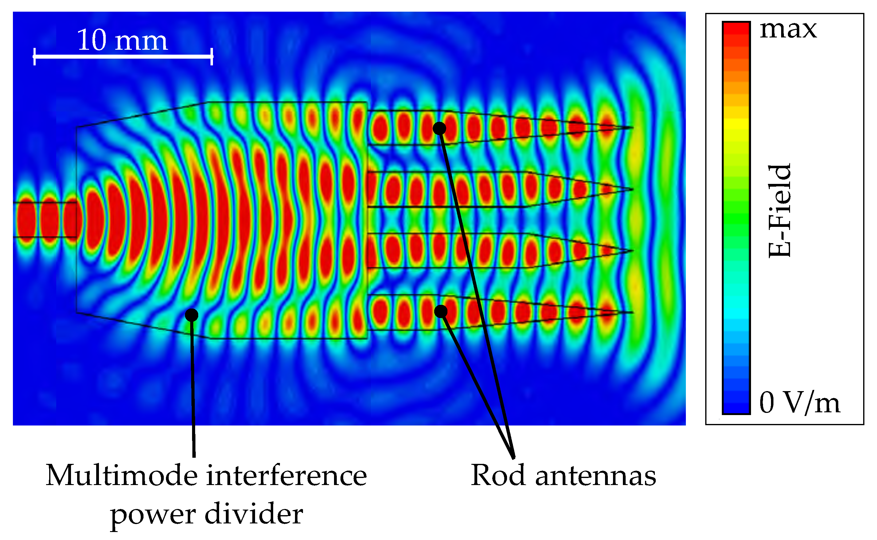
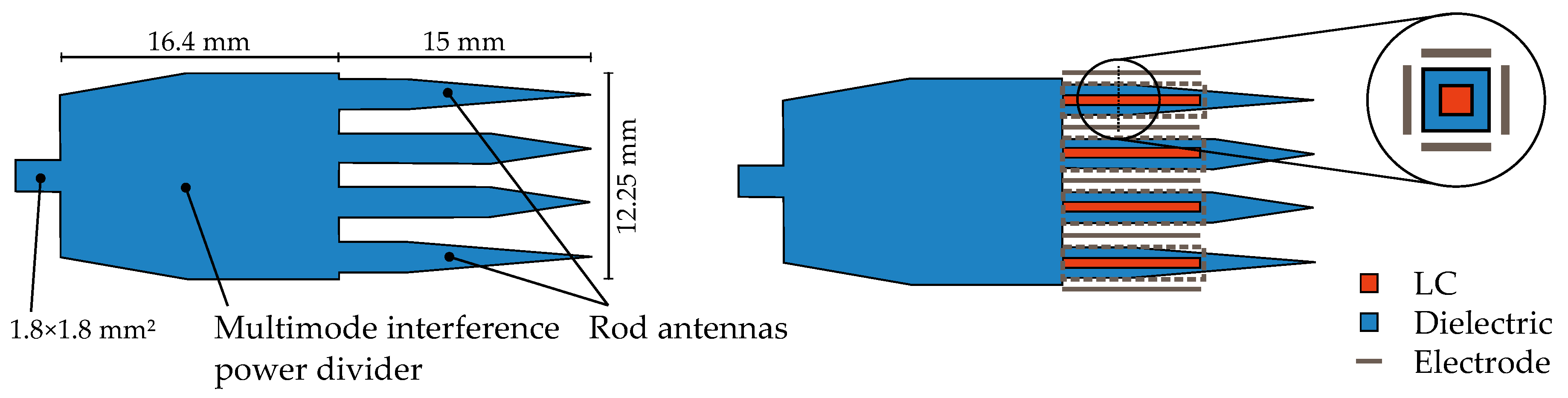
Another application could be the integration of the subwavelength fiber phase shifter in a fully dielectric phased array. In [44], a first fully dielectric antenna array was presented, see Figure 29. It consists of four dielectric rod antennas, which is also fed by a special multimode interference (MMI) power divider. Within this divider, multimode propagation is used to provide power splitting in one single step. Multiple maxima are formed due to the superposition and the different propagation constants of all propagable modes inside the waveguide. This interference phenomenon is visualized in Figure 30.
With the input position on the left, the interference phenomenon occurs in the broad waveguide section. It can be seen, that multiple field maxima are formed, with each single maximum feeding a rod antenna. This power divider allows a very compact design, where power splitting is achieved in one single step. This reduces the dielectric loss, and further, parasitic radiation. The next step will be the integration of LC-based subwavelength fiber phase shifters in the presented antenna array design. For this, LC can be directly inserted in the waveguide section before the rod antennas, see Figure 29. Although the LC integration can be realized quite easily, the main challenge will be the integration of the required biasing electrode as they can disturb the propagating electromagnetic wave. Furthermore, high permittivity plastics are in the focus of research for minimization of the antenna.
7. Conclusions
In this paper, a comprehensive review of the latest developments in microwave liquid crystal technology has been given. Starting from the material properties and their characterization, requirements for mmWave communication systems have been introduced. From these basic considerations, the necessity for electronic steerable antennas systems is derived. An energy efficient and high-performance realization uses liquid crystals as tunable dielectric. Above 60 GHz metallic rectangular waveguide components can usually provide highest performance. Due to the implementation of biasing electrodes, the performance degrades substantially. To overcome this problem, the dielectric waveguide technology, commonly known from optics, is adapted to millimeter waves. With this, an easy integration of biasing electrodes is possible. The first demonstrators presented in this paper show promising results. Table 3 shows an overview on different phase shifter realizations at W-band. The high potential of LC-based devices is obvious.
All given phase shifters are line phase shifter, which make them operate in a wide frequency band. Usually, MEMS and semiconductor phase shifters have response times in the range of , as exemplarily 15 in [45]. LC devices are suffering from comparatively high response times, as for example 340 in the best case for a loaded CPW line [46] and approximately 1 for the presented dielectric waveguide phase shifters. Further work includes optimization of components based on dielectric waveguides. Specific focus is on the fabrication of the devices and on LC integration. Here, modern additive manufacturing techniques can be implemented.
The tunable dielectric waveguide technology is one example for research beside LC material engineering. Material optimization is ongoing [9] and will stay a major task in future. The development of new tunable structures is the second major field of research. Recently, planar structures utilizing plasmonic or slow wave effects have been presented [53,54,55]. These structures show a huge potential, as they faciitate integration. Unfortunately, these types of components usually show high insertion losses. The main advantages compared to metallic rectangular and dielectric waveguides are much faster response times of the components. This is due to a much thinner LC layer which can be tuned faster with lower voltages. Also, substrate integrated waveguides (SIW) [56,57] will probably play a significant role in the future. The right technology has always to been chosen based on a tradeoff. Researchers in academia and industry are working hard iso that LC-based devices can manifest their large potential in many applications.
Author Contributions
Conceptualization: H.M., M.J., R.R. and E.P.; Investigation: M.J., R.R. and E.P.; Writing: H.M., M.J. and R.R.; Review & Editing, M.N., E.P. and R.J.; Supervision, H.M. and R.J.; Funding Acquisition, H.M. and M.J.
Funding
This research was partially funded by DFG grants JA921/68-1, MA6281/4-1, JA921/29-2 and BMWi/DLR under contract 50YB1113.
Acknowledgments
The authors gratefully acknowledge Merck KGaA and CST AG for supplying Liquid Crystal mixtures and CST Microwave Studio, respectively. We acknowledge support by the German Research Foundation and the Open Access Publishing Fund of Technische Universität Darmstadt.
Conflicts of Interest
The authors declare no conflict of interest.
Abbreviations
The following abbreviations are used in this manuscript:
| 5G | System for Mobile Communication of the 5th generation |
| Displacement field | |
| DC | Direct current |
| DW | Dielectric waveguide |
| Electric field | |
| effective permittivity | |
| effective permittivity of an LC volume for parallel alignment | |
| effective permittivity of an LC volume for perpendicular alignment | |
| FoM | Figure of Merit |
| GEO | geostationary orbit (satellite) |
| HPBW | Half-power beam width |
| IL | Insertion loss () |
| IP3 | Third-order intercept point |
| ITU | International Telecommunication Union |
| Ka-band | Communications band from 26.5–40 |
| Ku-band | Communications band from 12–18 |
| LC | Liquid Crystal |
| LCD | Liquid crystal display |
| LEO | low earth orbit (satellite) |
| MMI | Multimode interference |
| mmWave | Millimeter wave |
| OLED | Organic LED |
| PIM | Passive intermodulation |
| PET | Polyethylenterephthalat |
| PTFE | Polytetrafluorethylene (Teflon) |
| RF | Radio frequency |
| SIW | Substrate integrated waveguide |
| TDS | time-domain spectroscopy |
| TN | twisted nematic |
| UV | Ultra violet |
| VNA | Vector network analyzer |
| W-band | Communications band from 75–110 |
| WRC | World Radio Conference |
References
- Helfrich, W.; Schadt, M. Lichtsteuerzelle. Swiss Patent CH 532261, 1970. [Google Scholar]
- Fergason, L. Display Devices Utilizing Liquid Crystal Light Modulation. U.S. Patent 373,1986, 1971. [Google Scholar]
- De Gennes, P.G.; Prost, J. The Physics of Liquid Crystals; Oxford University Press: Oxford, UK, 1995. [Google Scholar]
- Allen, M.P. Molecular simulation and theory of liquid crystal surface anchoring. Mol. Phys. 1999, 96, 1391–1397. [Google Scholar] [CrossRef]
- Yokoyama, H. Surface Anchoring of Nematic Liquid Crystals. Mol. Cryst. Liq. Cryst. Incorp. Nonlinear Opt. 1988, 165, 265–316. [Google Scholar] [CrossRef]
- Yang, D.K.; Wu, S.T. Fundamentals of Liquid Crystal Devices; John Wiley & Sons: Chichester, UK, 2006. [Google Scholar]
- Goelden, F.; Mueller, S.; Scheele, P.; Wittek, M.; Jakoby, R. IP3 Measurements of Liquid Crystals at Microwave Frequencies. In Proceedings of the 2006 European Microwave Conference, Manchester, UK, 10–15 September 2006. [Google Scholar] [CrossRef]
- Gäbler, A. Synthese steuerbarer Hochfrequenzschaltungen und Analyse Flüssigkristall-Basierter Leitungsphasenschieber in Gruppenantennen für Satellitenanwendungen im Ka-Band. Ph.D. Thesis, Technische Universität Darmstadt, Darmstadt, Germany, 2013. [Google Scholar]
- Fritzsch, C.; Wittek, M. Recent developments in liquid crystals for microwave applications. In Proceedings of the 2017 IEEE International Symposium on Antennas and Propagation & USNC/URSI National Radio Science Meeting, San Diego, CA, USA, 9–14 July 2017. [Google Scholar] [CrossRef]
- Weickhmann, C.; Jakoby, R.; Constable, E.; Lewis, R.A. Time-domain spectroscopy of novel nematic liquid 422 crystals in the terahertz range. In Proceedings of the International Conference on Infrared, Millimeter, and Terahertz Waves 423 (IRMMW-THz), Mainz, Germany, 1–6 Sepember 2013. [Google Scholar] [CrossRef]
- Weickhmann, C. Liquid Crystals towards Terahertz: Characterisation and Tunable Waveguide Phase Shifters for Millimetre-Wave and Terahertz Beamsteering Antennas. Ph.D. Thesis, Technische Universität Darmstadt, Darmstadt, Germany, 2017. [Google Scholar]
- Li, X.; Gani, A.; Salleh, R.; Zakaria, O. The Future of Mobile Wireless Communication Networks. In Proceedings of the 2009 International Conference on Communication Software and Networks, Macau, China, 27–28 February 2009. [Google Scholar] [CrossRef]
- Fettweis, G.; Alamouti, S. 5G: Personal mobile internet beyond what cellular did to telephony. IEEE Commun. Mag. 2014, 52, 140–145. [Google Scholar] [CrossRef]
- Simsek, M.; Aijaz, A.; Dohler, M.; Sachs, J.; Fettweis, G. 5G-Enabled Tactile Internet. IEEE J. Sel. Areas Commun. 2016, 34, 460–473. [Google Scholar] [CrossRef] [Green Version]
- Rappaport, T.S.; Sun, S.; Mayzus, R.; Zhao, H.; Azar, Y.; Wang, K.; Wong, G.N.; Schulz, J.K.; Samimi, M.; Gutierrez, F. Millimeter Wave Mobile Communications for 5G Cellular: It Will Work! IEEE Access 2013, 1, 335–349. [Google Scholar] [CrossRef] [Green Version]
- Lee, J.; Song, Y.; Choi, E.; Park, J. mmWave cellular mobile communication for Giga Korea 5G project. In Proceedings of the 2015 Asia-Pacific Conference on Communications (APCC), Kyoto, Japan, 14–16 October 2015. [Google Scholar] [CrossRef]
- FierceWireless. KT’s Millimeter Wave 5G Network Transmitted 3,800 TB of Data during Winter Olympics. 2018. Available online: https://www.fiercewireless.com/5g/kt-s-millimeter-wave-5g-network-transmitted-3-800-tb-data-during-winter-olympics (accessed on 24 August 2018).
- ITU Recommendation. Attenuation by Atmospheric Gases (ITU-R P.676-11). 2016. Available online: https://www.itu.int/rec/R-REC-P.676 (accessed on 24 August 2018).
- ITU Recommendation. Specific Attenuation Model for Rain for Use in Prediction Methods (ITU-R P.838-3). 2005. Available online: https://www.itu.int/rec/R-REC-P.838 (accessed on 24 August 2018).
- Gevorgian, S. Ferroelectrics in Microwave Devices, Circuits and Systems; Springer: London, UK, 2009. [Google Scholar]
- Paolis, R.D.; Coccetti, F.; Payan, S.; Maglione, M.; Guegan, G. Characterization of ferroelectric BST MIM capacitors up to 65 GHz for a compact phase shifter at 60 GHz. In Proceedings of the 2014 European Microwave Conference, Rome, Italy, 6–9 October 2014. [Google Scholar] [CrossRef]
- Paolis, R.D.; Payan, S.; Maglione, M.; Guegan, G.; Coccetti, F. High-Tunability and High-Q-Factor Integrated Ferroelectric Circuits up to Millimeter Waves. IEEE Trans. Microw. Theory Tech. 2015, 63, 2570–2578. [Google Scholar] [CrossRef]
- Shi, S.; Purden, J.; Lin, J.; York, R.A. A 24 GHz wafer scale electronically scanned antenna using BST phase shifters for collision avoidance systems. In Proceedings of the IEEE Antennas and Propagation Society International Symposium, Washington, DC, USA, 3–8 July 2005. [Google Scholar] [CrossRef]
- Zhang, M.; Liu, M.; Ling, S.; Chen, P.; Zhu, X.; Yu, X. K-band tunable phase shifter with microstrip line structure using BST technology. In Proceedings of the 2015 Asia-Pacific Microwave Conference (APMC), Nanjing, China, 6–9 December 2015. [Google Scholar] [CrossRef]
- Choi, K.; Courreges, S.; Zhao, Z.; Papapolymerou, J.; Hunt, A. X-band and Ka-band tunable devices using low-loss BST ferroelectric capacitors. In Proceedings of the 2009 IEEE International Symposium on the Applications of Ferroelectrics, Xi’an, China, 23–27 August 2009. [Google Scholar] [CrossRef]
- Wang, Z.; Song, Y.Y.; Sun, Y.; Bevivino, J.; Wu, M.; Veerakumar, V.; Fal, T.J.; Camley, R.E. Millimeter wave phase shifter based on ferromagnetic resonance in a hexagonal barium ferrite thin film. Appl. Phys. Lett. 2010, 97, 072509. [Google Scholar] [CrossRef]
- Patton, C.E. Hexagonal ferrite materials for phase shifter applications at millimeter wave frequencies. IEEE Trans. Magn. 1988, 24, 2024–2028. [Google Scholar] [CrossRef]
- Nafe, A.; Shamim, A. An Integrable SIW Phase Shifter in a Partially Magnetized Ferrite LTCC Package. IEEE Trans. Microw. Theory Tech. 2015, 63, 2264–2274. [Google Scholar] [CrossRef]
- Chakraborty, A.; Gupta, B. Paradigm Phase Shift: Rf Mems Phase Shifters: An Overview. IEEE Microw. Mag. 2017, 18, 22–41. [Google Scholar] [CrossRef]
- Shah, U.; Decrossas, E.; Jung-Kubiak, C.; Reck, T.; Chattopadhyay, G.; Mehdi, I.; Oberhammer, J. Submillimeter-Wave 3.3-bit RF MEMS Phase Shifter Integrated in Micromachined Waveguide. IEEE Trans. Terahertz Sci. Technol. 2016, 1–10. [Google Scholar] [CrossRef] [Green Version]
- Hillman, C.; Stupar, P.; Griffith, Z. Scaleable vanadium dioxide switches with submillimeterwave bandwidth: VO2 switches with impoved RF bandwidth and power handling. In Proceedings of the 2017 IEEE Compound Semiconductor Integrated Circuit Symposium (CSICS), Miami, FL, USA, 22–25 October 2017. [Google Scholar] [CrossRef]
- Huitema, L.; Crunteanu, A.; Wong, H.; Arnaud, E. Highly integrated VO2-based tunable antenna for millimeter-wave applications. Appl. Phys. Lett. 2017, 110, 203501. [Google Scholar] [CrossRef]
- Norooziarab, M.; Bulja, S.; Cahill, R.; Kopf, R.; Hu, T.C.; Tate, A. Variable Temperature Broadband Microwave and Millimeter-Wave Characterization of Electrochromic (WO3/LiNbO3/NiO) Thin Films. IEEE Trans. Microw. Theory Tech. 2018, 66, 1070–1080. [Google Scholar] [CrossRef]
- Tebbe, M.; Hoehn, A.; Nathrath, N.; Weickhmann, C. Simulation of an electronically steerable horn antenna array with liquid crystal phase shifters. In Proceedings of the 2016 IEEE Aerospace Conference, Big Sky, MT, USA, 5–12 March 2016. [Google Scholar] [CrossRef]
- Karabey, O.H.; Gaebler, A.; Strunck, S.; Jakoby, R. A 2-D Electronically Steered Phased-Array Antenna With 2x2 Elements in LC Display Technology. IEEE Trans. Microw. Theory Tech. 2012, 60, 1297–1306. [Google Scholar] [CrossRef]
- Weickhmann, C.; Nathrath, N.; Gehring, R.; Gaebler, A.; Jost, M.; Jakoby, R. A light-weight tunable liquid crystal phase shifter for an efficient phased array antenna. In Proceedings of the 2013 European Microwave Conference, Nuremberg, Germany, 6–10 October 2013; pp. 428–431. [Google Scholar] [CrossRef]
- Tebbe, M.; Hoehn, A.; Nathrath, N.; Weickhmann, C. Manufacturing and testing of liquid crystal phase shifters for an electronically steerable array. In Proceedings of the 2017 IEEE Aerospace Conference, Big Sky, MT, USA, 4–11 March 2017. [Google Scholar] [CrossRef]
- Jost, M.; Gaebler, A.; Weickhmann, C.; Strunck, S.; Hu, W.; Karabey, O.H.; Jakoby, R. Evolution of Microwave Nematic Liquid Crystal Mixtures and Development of Continuously Tuneable Micro- and Millimetre Wave Components. Mol. Cryst. Liq. Cryst. 2015, 610, 173–186. [Google Scholar] [CrossRef]
- Jost, M.; Fritzsch, C.; Karabey, O.H.; Weickhmann, C.; Jakoby, R.; Gäbler, A.; Strunck, S. Liquid crystal based low-loss phase shifter for W-band frequencies. Electron. Lett. 2013, 49, 1460–1462. [Google Scholar] [CrossRef]
- Hirvonen, T.M.; Vainikainen, P.; Lozowski, A.; Raisanen, A.V. Measurement of dielectrics at 100 GHz with an open resonator connected to a network analyzer. IEEE Trans. Instrum. Meas. 1996, 45, 780–786. [Google Scholar] [CrossRef]
- Jost, M.; Weickhmann, C.; Strunck, S.; Gaebler, A.; Hu, W.; Franke, T.; Prasetiadi, A.E.; Karabey, O.H.; Jakoby, R. Electrically biased W-band phase shifter based on liquid crystal. In Proceedings of the 2014 International Conference on Infrared, Millimeter, and Terahertz waves (IRMMW-THz), Tucson, AZ, USA, 14–19 September 2014. [Google Scholar] [CrossRef]
- Reese, R.; Jost, M.; Maune, H.; Jakoby, R. Design of a continuously tunable W-band phase shifter in dielectric waveguide topology. In Proceedings of the 2017 IEEE MTT-S International Microwave Symposium (IMS), Honololu, HI, USA, 4–9 June 2017. [Google Scholar] [CrossRef]
- Jost, M.; Reese, R.; Nickel, M.; Maune, H.; Jakoby, R. Fully dielectric interference-based SPDT with liquid crystal phase shifters. IET Microw. Antennas Propag. 2018, 12, 850–857. [Google Scholar] [CrossRef]
- Reese, R.; Jost, M.; Nickel, M.; Polat, E.; Jakoby, R.; Maune, H. A Fully Dielectric Lightweight Antenna Array Using a Multimode Interference Power Divider at W-Band. IEEE Antennas Wirel. Propag. Lett. 2017, 16, 3236–3239. [Google Scholar] [CrossRef]
- Stehle, A.; Georgiev, G.; Ziegler, V.; Schoenlinner, B.; Prechtel, U.; Seidel, H.; Schmid, U. RF-MEMS Switch and Phase Shifter Optimized for W-Band. In Proceedings of the 2008 38th European Microwave Conference, Amsterdam, The Netherlands, 27–31 October 2008; pp. 104–107. [Google Scholar] [CrossRef]
- Goelden, F.; Gaebler, A.; Goebel, M.; Manabe, A.; Mueller, S.; Jakoby, R. Tunable liquid crystal phase shifter for microwave frequencies. Electron. Lett. 2009, 45, 686. [Google Scholar] [CrossRef]
- Margomenos, A.; Kurdoghlian, A.; Micovic, M.; Shinohara, K.; Moyer, H.; Regan, D.C.; Grabar, R.M.; McGuire, C.; Wetzel, M.D.; Chow, D.H. W-Band GaN Receiver Components Utilizing Highly Scaled, Next Generation GaN Device Technology. In Proceedings of the 2014 IEEE Compound Semiconductor Integrated Circuit Symposium (CSICS), La Jolla, CA, USA, 19–22 October 2014; pp. 1–4. [Google Scholar] [CrossRef]
- Kim, H.T.; Park, J.H.; Lee, S.; Kim, S.; Kim, J.M.; Kim, Y.K.; Kwon, Y. V-band 2-b and 4-b low-loss and low-voltage distributed MEMS digital phase shifter using metal-air-metal capacitors. IEEE Trans. Microw. Theory Tech. 2002, 50, 2918–2923. [Google Scholar] [CrossRef]
- Psychogiou, D.; Li, Y.; Hesselbarth, J.; Kuehne, S.; Peroulis, D.; Hierold, C.; Hafner, C. Millimeter-wave phase shifter based on waveguide-mounted RF-MEMS. Microw. Opt. Technol. Lett. 2013, 55, 465–468. [Google Scholar] [CrossRef]
- Chang, C.C.; Chen, Y.C.; Hsieh, S.C. A V-Band Three-State Phase Shifter in CMOS-MEMS Technology. IEEE Microw. Wirel. Compon. Lett. 2013, 23, 264–266. [Google Scholar] [CrossRef]
- Mueller, S.; Goelden, F.; Scheele, P.; Wittek, M.; Hock, C.; Jakoby, R. Passive Phase Shifter for W-Band Applications using Liquid Crystals. In Proceedings of the 2006 European Microwave Conference, Manchester, UK, 10–15 September 2006; pp. 306–309. [Google Scholar] [CrossRef]
- Fritzsch, C.; Giacomozzi, F.; Karabey, O.H.; Goelden, F.; Moessinger, A.; Bildik, S.; Colpo, S.; Jakoby, R. Continuously tunable W-band phase shifter based on liquid crystals and MEMS technology. In Proceedings of the 2011 41st European Microwave Conference (EuMC), Manchester, UK, 10–11 October 2011; pp. 1083–1086. [Google Scholar]
- Gorkunov, M.; Kasyanova, I.; Artemov, V.; Barnik, M.; Geivandov, A.; Palto, S. Fast Surface-Plasmon-Mediated Electro-Optics of a Liquid Crystal on a Metal Grating. Phys. Rev. Appl. 2017, 8. [Google Scholar] [CrossRef]
- Jost, M.; Gautam, J.S.K.; Gomes, L.G.; Reese, R.; Polat, E.; Nickel, M.; Pinheiro, J.M.; Serrano, A.L.C.; Maune, H.; Rehder, G.P.; et al. Miniaturized Liquid Crystal Slow Wave Phase Shifter Based on Nanowire Filled Membranes. IEEE Microw. Wirel. Compon. Lett. 2018, 28, 681–683. [Google Scholar] [CrossRef]
- Buchnev, O.; Podoliak, N.; Kaczmarek, M.; Zheludev, N.I.; Fedotov, V.A. Electrically Controlled Nanostructured Metasurface Loaded with Liquid Crystal: Toward Multifunctional Photonic Switch. Adv. Opt. Mater. 2015, 3, 674–679. [Google Scholar] [CrossRef] [Green Version]
- Prasetiadi, A.E.; Rahmawati, S.; Weickhmann, C.; Nickel, M.; Jost, M.; Franke, T.; Hu, W.; Maune, H.; Jakoby, R. Electrical biasing scheme for Liquid-Crystal-based tunable Substrate Integrated Waveguide structures. In Proceedings of the 2016 German Microwave Conference (GeMiC), Bochum, Germany, 14–16 March 2016. [Google Scholar] [CrossRef]
- Prasetiadi, A.E.; Franke, T.; Jakoby, R.; Nickel, M.; Karabey, O.H.; Hu, W.; Weickhmann, C.; Jost, M. Continuously tunable substrate integrated waveguide bandpass filter in liquid crystal technology with magnetic biasing. Electron. Lett. 2015, 51, 1584–1585. [Google Scholar] [CrossRef]
Figure 1.
Working principle of a TN-cell used in LCDs. (Right) the unbiased LC rotates polarization by 90. The light can pass two twisted polarization grids and the pixel is on. When the LC is biased (Left), the polarization of light is not rotated. Hence, the pixel is off as the light cannot pass the second polarization grid.
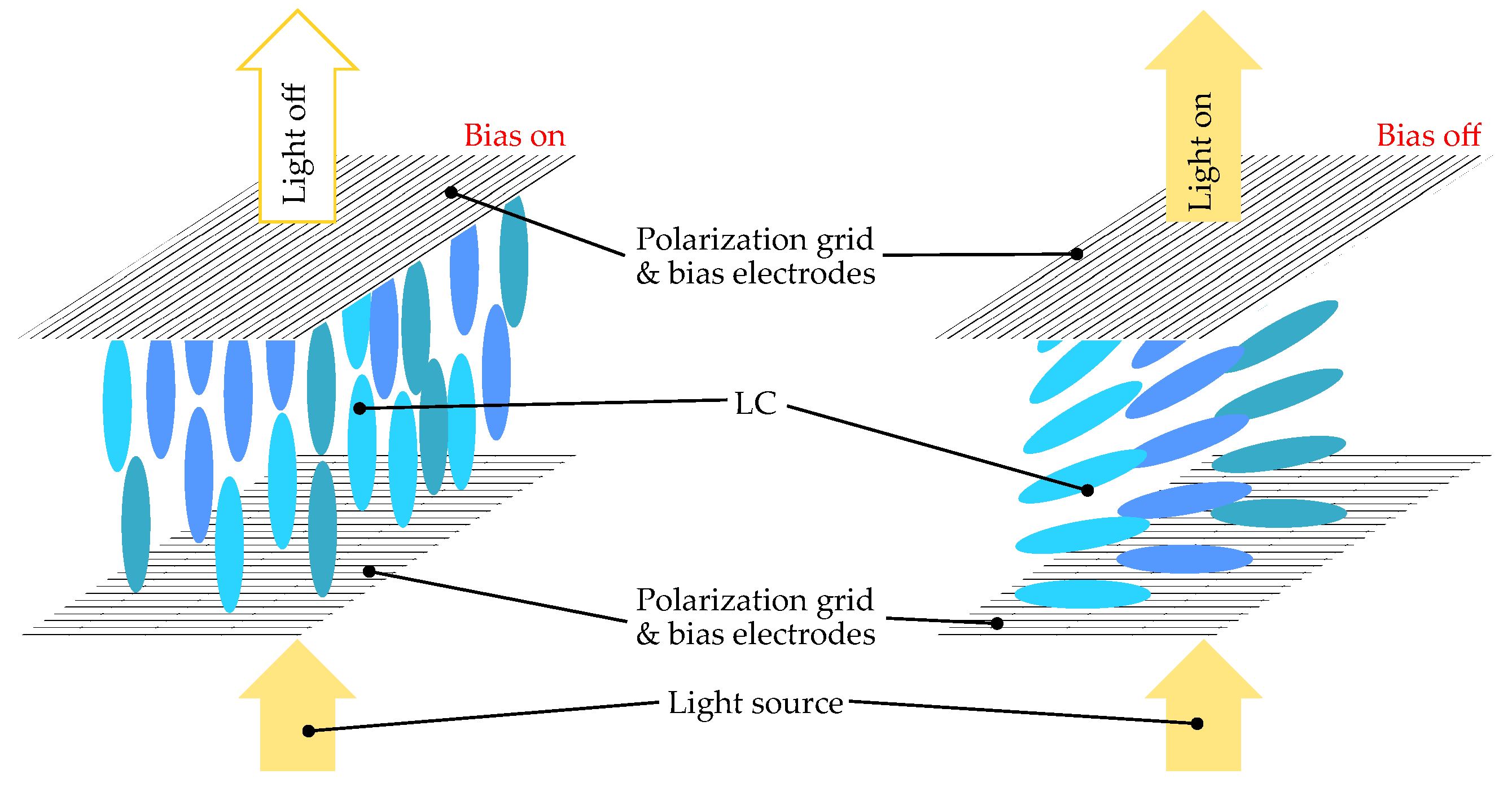
Figure 2.
Overview on different phases of nematic liquid crystals. (Left) shows the material’s crystalline structure and the resulting permittivity for different orientations. In the (Right) picture the different phases can be differentiated by the LC’s optical properties.
Figure 2.
Overview on different phases of nematic liquid crystals. (Left) shows the material’s crystalline structure and the resulting permittivity for different orientations. In the (Right) picture the different phases can be differentiated by the LC’s optical properties.
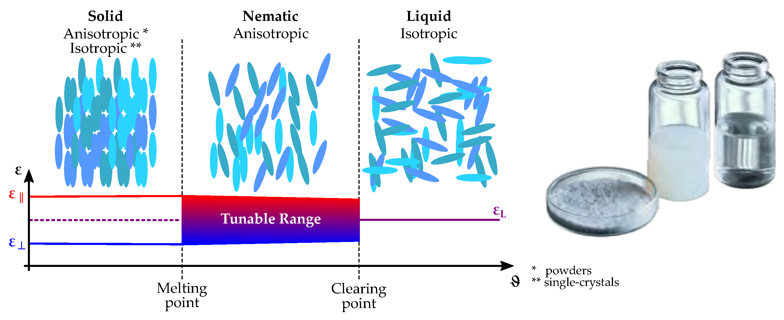
Figure 3.
Definition of the director for a single LC unit volume element in the device’s coordinate system () and relation to the permittivities defined in the material’s coordinate system () with the material properties , and the macroscopic unit volume properties , .
Figure 3.
Definition of the director for a single LC unit volume element in the device’s coordinate system () and relation to the permittivities defined in the material’s coordinate system () with the material properties , and the macroscopic unit volume properties , .

Figure 4.
Idealized parallel-plate capacitor with LC as dielectric filling for the three cases defined in Equation (7), (Left) , (Right) , and (Center) “else”. Note: Interface effects between LC and electrodes are neglected for simplification.
Figure 4.
Idealized parallel-plate capacitor with LC as dielectric filling for the three cases defined in Equation (7), (Left) , (Right) , and (Center) “else”. Note: Interface effects between LC and electrodes are neglected for simplification.
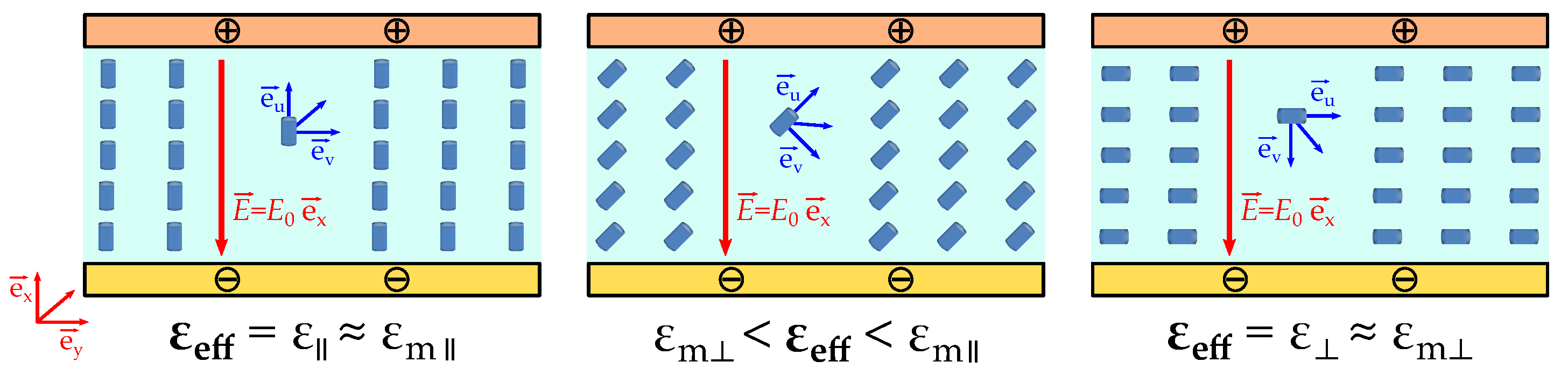
Figure 5.
Possible combinations of different orientation mechanisms with state I and II at top and bottom, respectively: (Left) combination of surface anchoring and electric actuation as used for planar devices; (Center) both electric actuations as used in waveguide components and (Right) both magnetic actuations as used for material characterization.

Figure 6.
Resonator setup for dual mode LC characterization based on the cavity perturbation technique at 19 GHz.
Figure 6.
Resonator setup for dual mode LC characterization based on the cavity perturbation technique at 19 GHz.
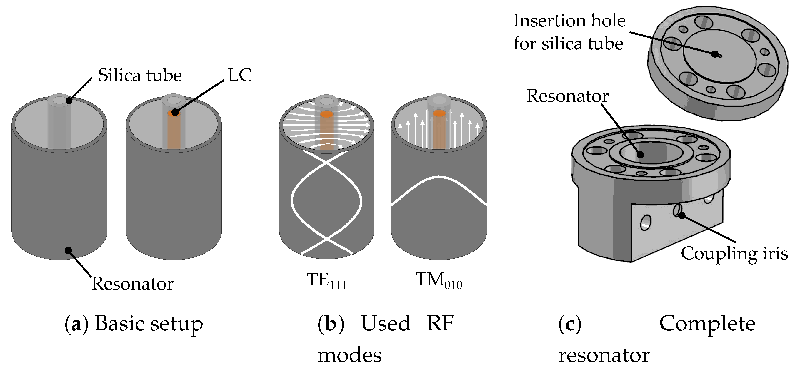
Figure 7.
Development of LC’s microwave properties at 19 GHz from the early 2000’s where first display LCs have been used towards recent LC mixtures specifically synthesized for microwave applications. The mixtures were measured at room temperature.
Figure 7.
Development of LC’s microwave properties at 19 GHz from the early 2000’s where first display LCs have been used towards recent LC mixtures specifically synthesized for microwave applications. The mixtures were measured at room temperature.

Figure 8.
Schematic of a time-domain spectroscopy THz measurement system as used in [10] for LC characterization. By comparing the measurement results of an empty and a LC-filled sample holder, the dielectric properties of LC can be determined.
Figure 8.
Schematic of a time-domain spectroscopy THz measurement system as used in [10] for LC characterization. By comparing the measurement results of an empty and a LC-filled sample holder, the dielectric properties of LC can be determined.

Figure 9.
THz characterization results for the LC GT3-23001 from Merck KGaA, Darmstadt, Germany.

Figure 10.
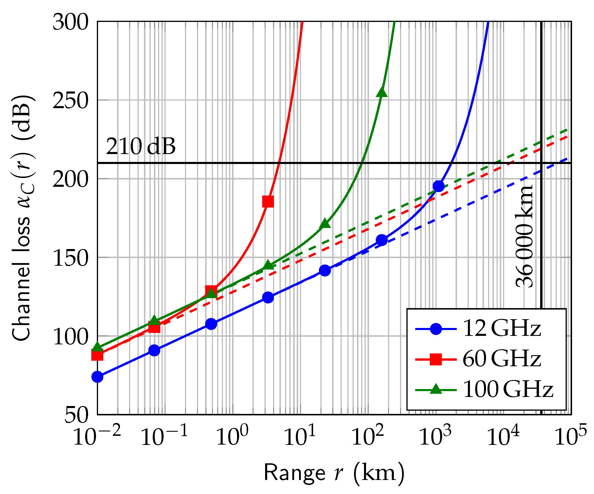
Channel loss for different frequencies as sum of free space path loss (dashed lines) and the atmospheric attenuation according to ITU standard atmosphere (solid lines) for homogenous medium between transmitter and receiver. As reference the properties of a geostationary satellite for broadcasting at Ku-band (12 GHz) with 36,000 km transmission range with approximately 210 dB of insertion loss are highlighted.
Figure 10.
Channel loss for different frequencies as sum of free space path loss (dashed lines) and the atmospheric attenuation according to ITU standard atmosphere (solid lines) for homogenous medium between transmitter and receiver. As reference the properties of a geostationary satellite for broadcasting at Ku-band (12 GHz) with 36,000 km transmission range with approximately 210 dB of insertion loss are highlighted.

Figure 11.
Possible implementation of the weighting functions for array antennas. The block diagrams are simplified in such a way that all components and stages not essential for signal weighting are neglected.
Figure 11.
Possible implementation of the weighting functions for array antennas. The block diagrams are simplified in such a way that all components and stages not essential for signal weighting are neglected.
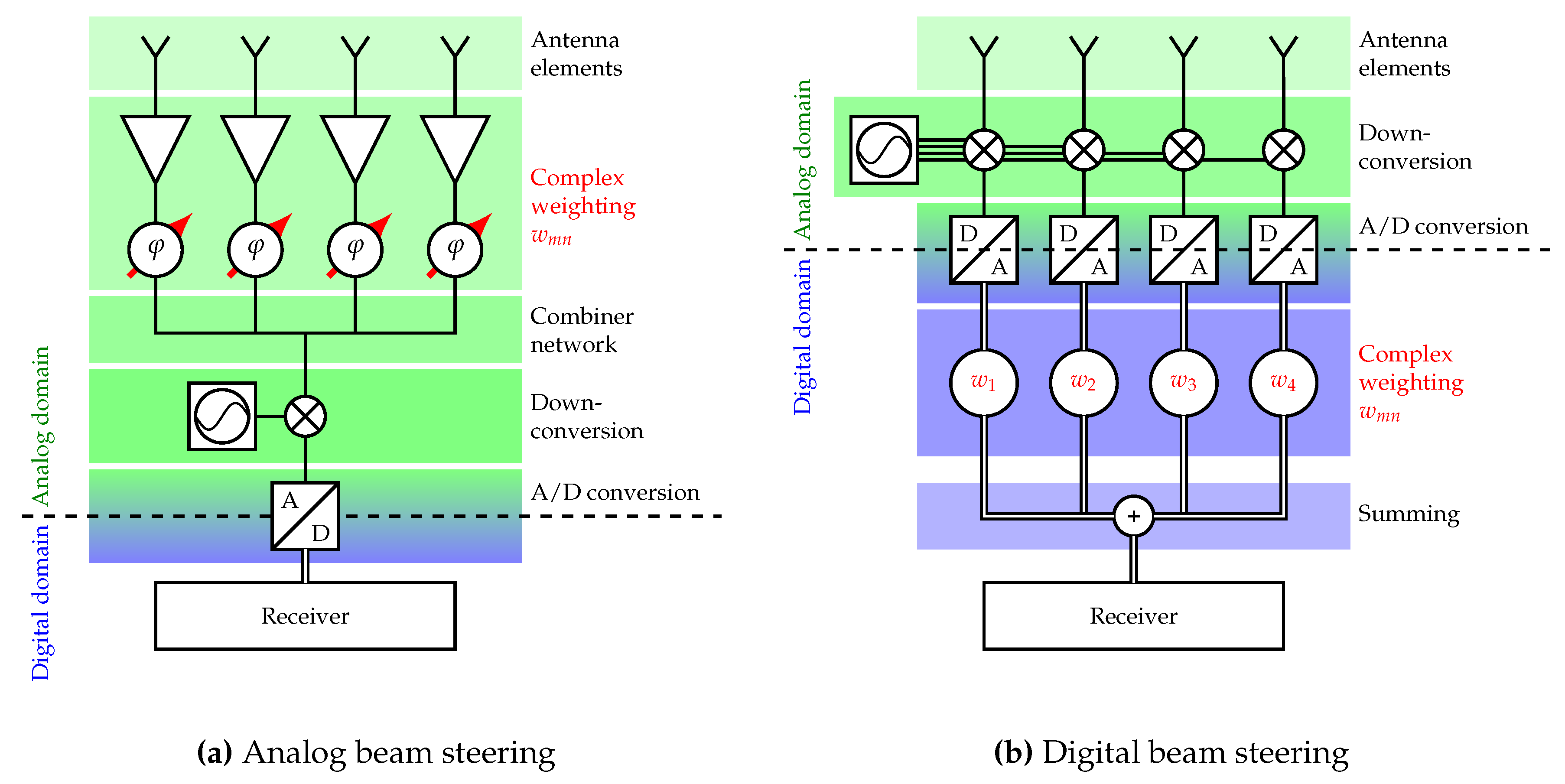
Figure 12.
Planar Antenna with LC enabled beam steering. (Left) early demonstrator of an array published in [35] with (top left) the measured beam pattern at 17.5 GHz with a antenna gain of 6 dB realized by phase shifters with a FoM of 90/dB. (Right) prototype of an sub-array realized in thin film LC technology. The complete antenna consists of 16 panels and shows a gain of 30 with a steering range of .
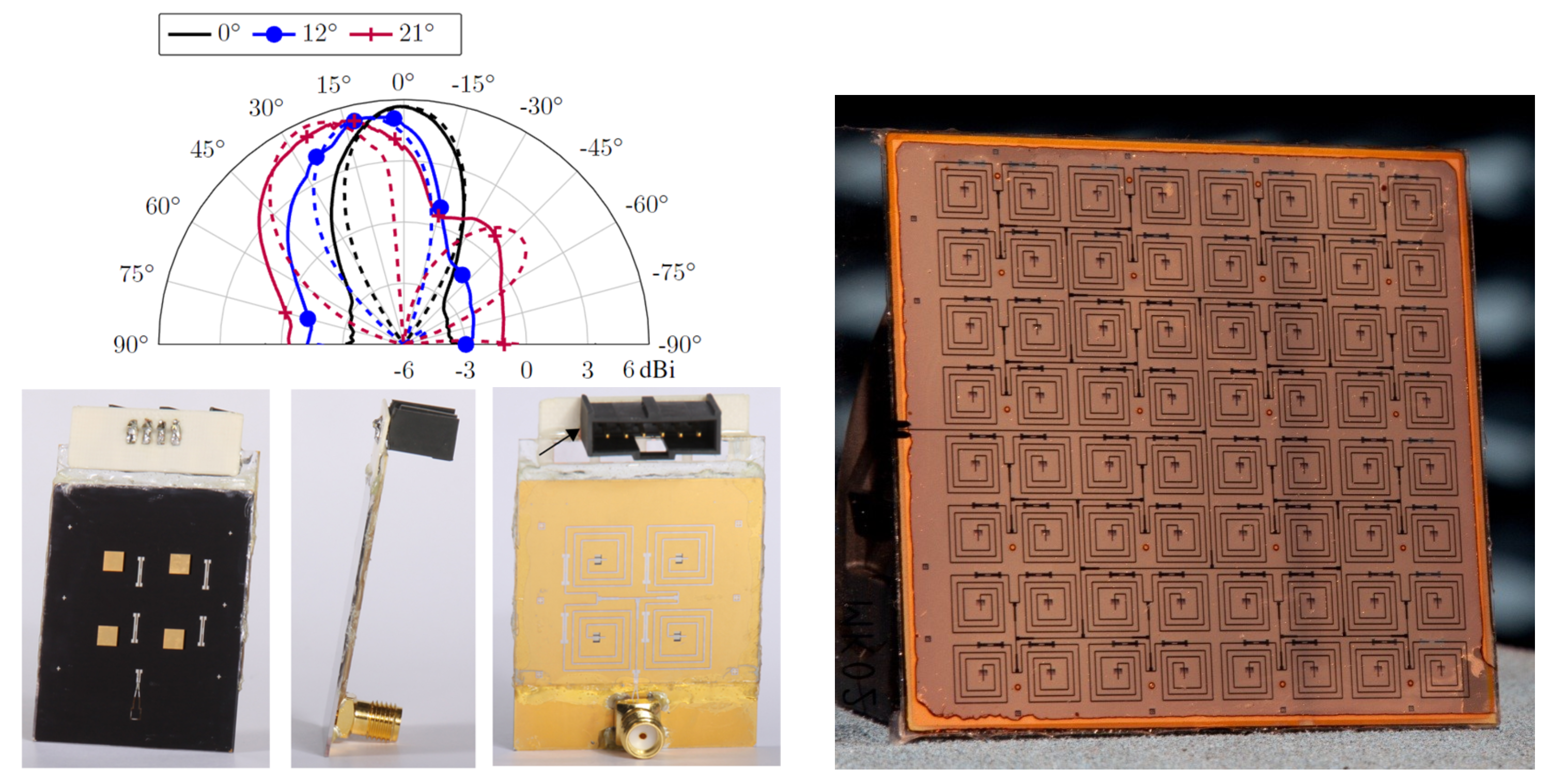
Figure 13.
Schematic cross section of the metallic rectangular waveguide LC phase shifter with partial LC filling.
Figure 13.
Schematic cross section of the metallic rectangular waveguide LC phase shifter with partial LC filling.

Figure 14.
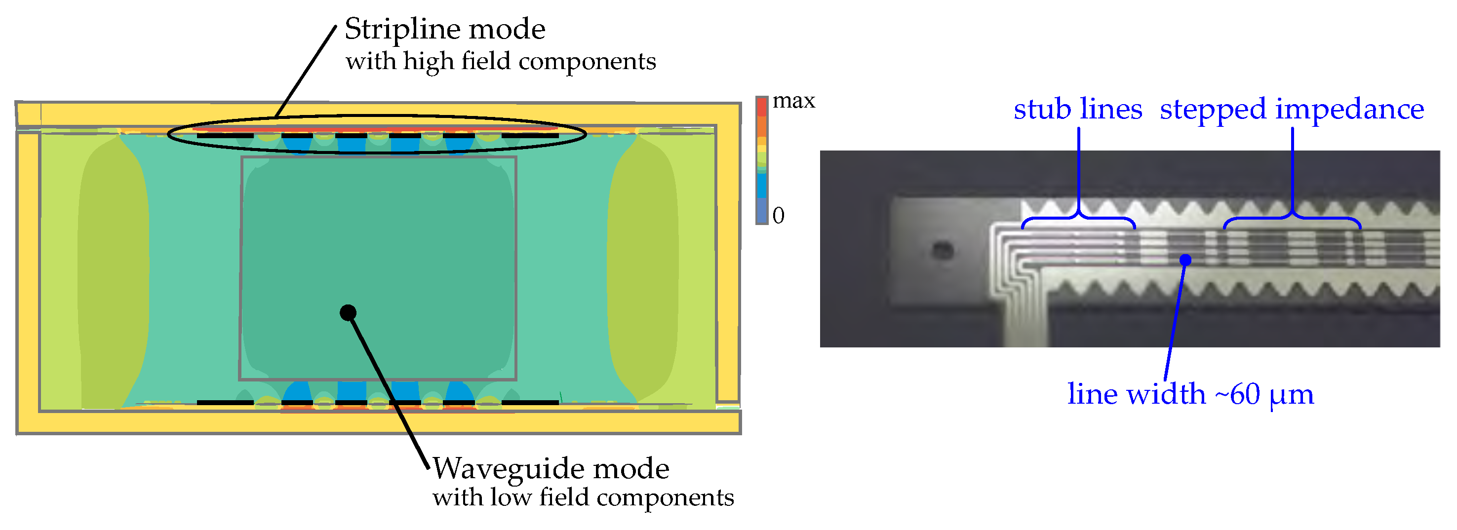
(Left) Field intensity of the guided modes within the dielectrically filled waveguide phase shifter for the case of straight biasing electrodes. Most power is confined in the TEM stripline mode, while nearly no power is in the fundamental TE10 waveguide mode. (Right) Biasing electrodes with stepped-impedance structures and -stub lines for strip mode suppression.
Figure 14.
(Left) Field intensity of the guided modes within the dielectrically filled waveguide phase shifter for the case of straight biasing electrodes. Most power is confined in the TEM stripline mode, while nearly no power is in the fundamental TE10 waveguide mode. (Right) Biasing electrodes with stepped-impedance structures and -stub lines for strip mode suppression.

Figure 15.
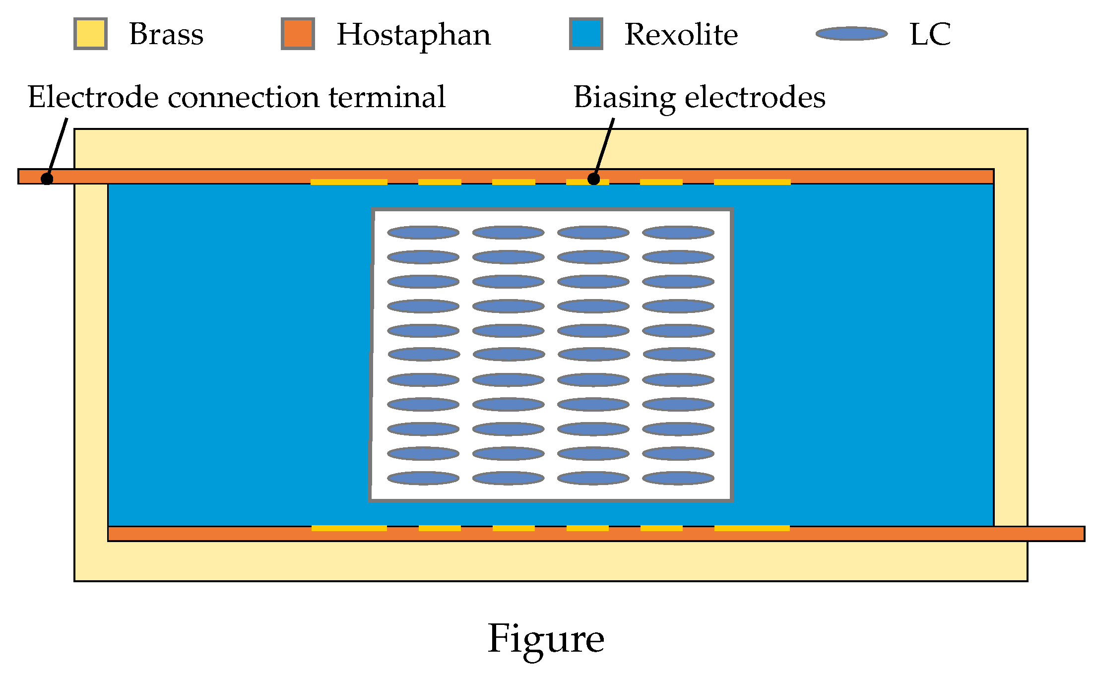
Split-block design of the magnetically biased W-band rectangular waveguide phase shifter based on LC. The dimensions of the split-block are .
Figure 15.
Split-block design of the magnetically biased W-band rectangular waveguide phase shifter based on LC. The dimensions of the split-block are .
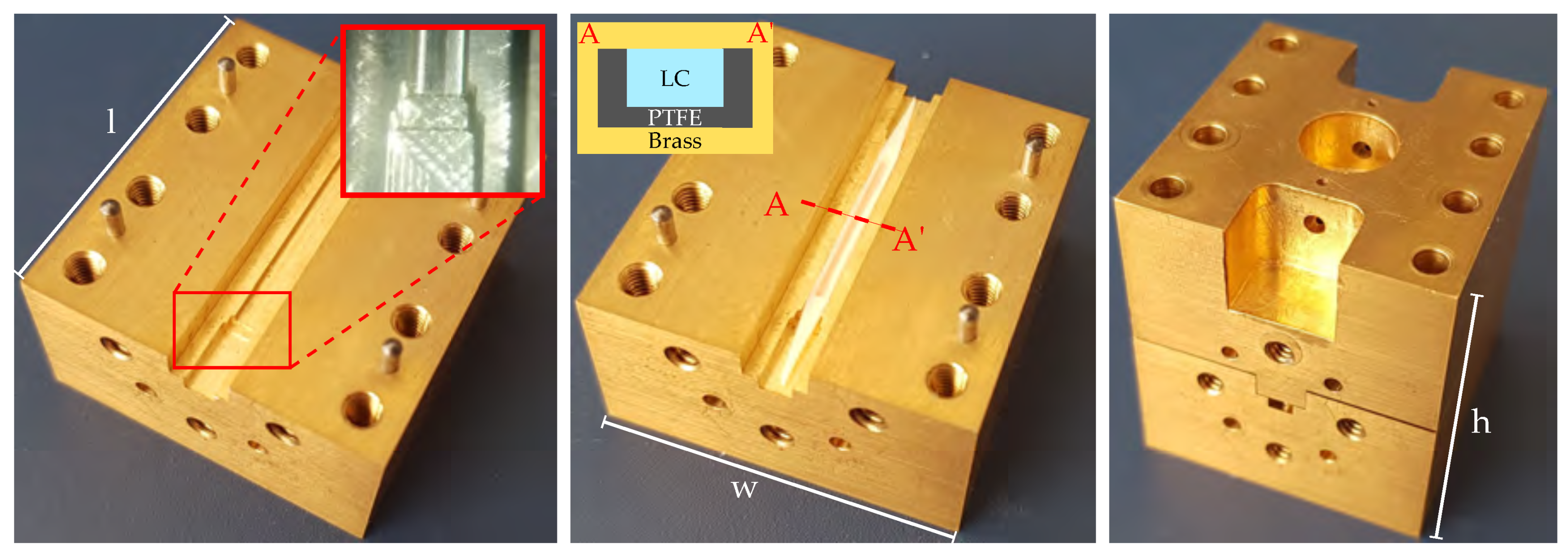
Figure 16.
(Left) Cross section and (Right) measurement setup for the magnetically biased W-band rectangular waveguide phase shifter.
Figure 16.
(Left) Cross section and (Right) measurement setup for the magnetically biased W-band rectangular waveguide phase shifter.
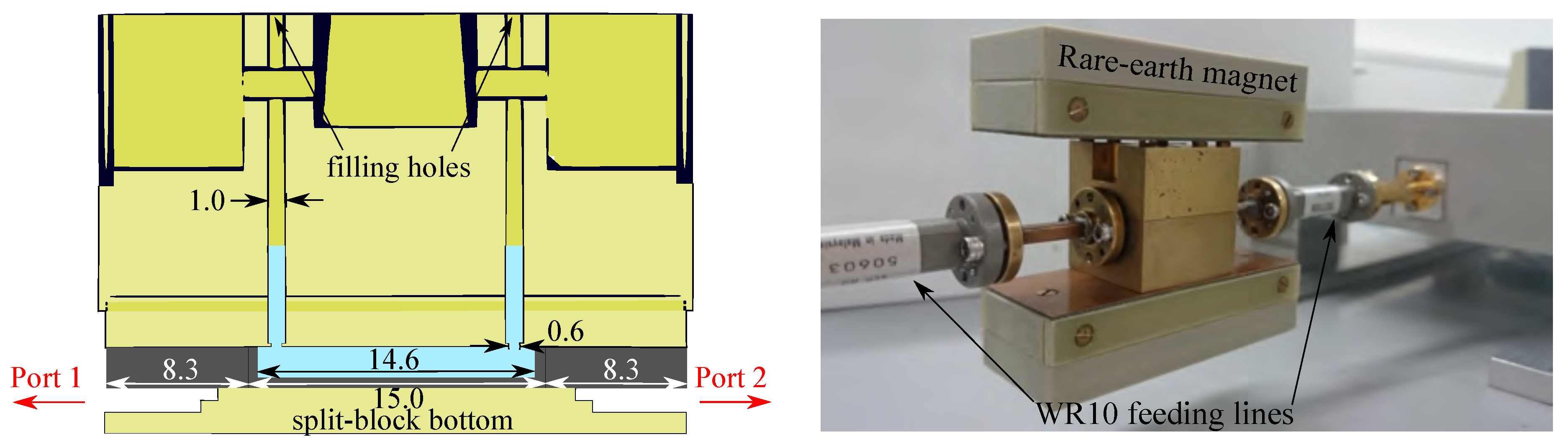
Figure 17.
Measured (solid) and simulated (dashed) results of the magnetically biased W-band rectangular waveguide phase shifter based on LC.
Figure 17.
Measured (solid) and simulated (dashed) results of the magnetically biased W-band rectangular waveguide phase shifter based on LC.
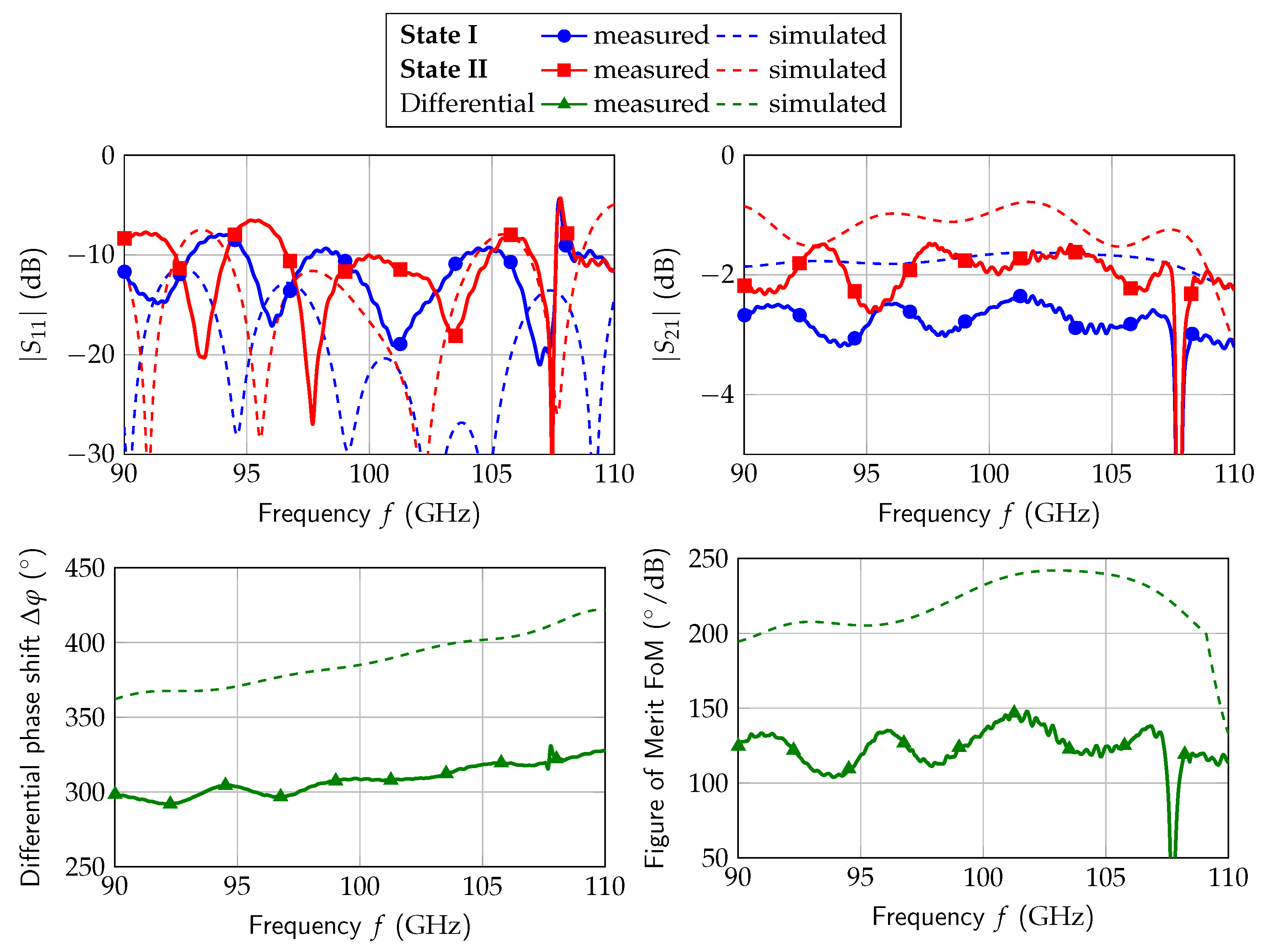
Figure 18.
Simulated field distribution of the electrically biased W-band rectangular waveguide phase shifter based on LC.
Figure 18.
Simulated field distribution of the electrically biased W-band rectangular waveguide phase shifter based on LC.

Figure 19.
Split-block design of the electrically biased W-band rectangular waveguide phase shifter based on LC.
Figure 19.
Split-block design of the electrically biased W-band rectangular waveguide phase shifter based on LC.
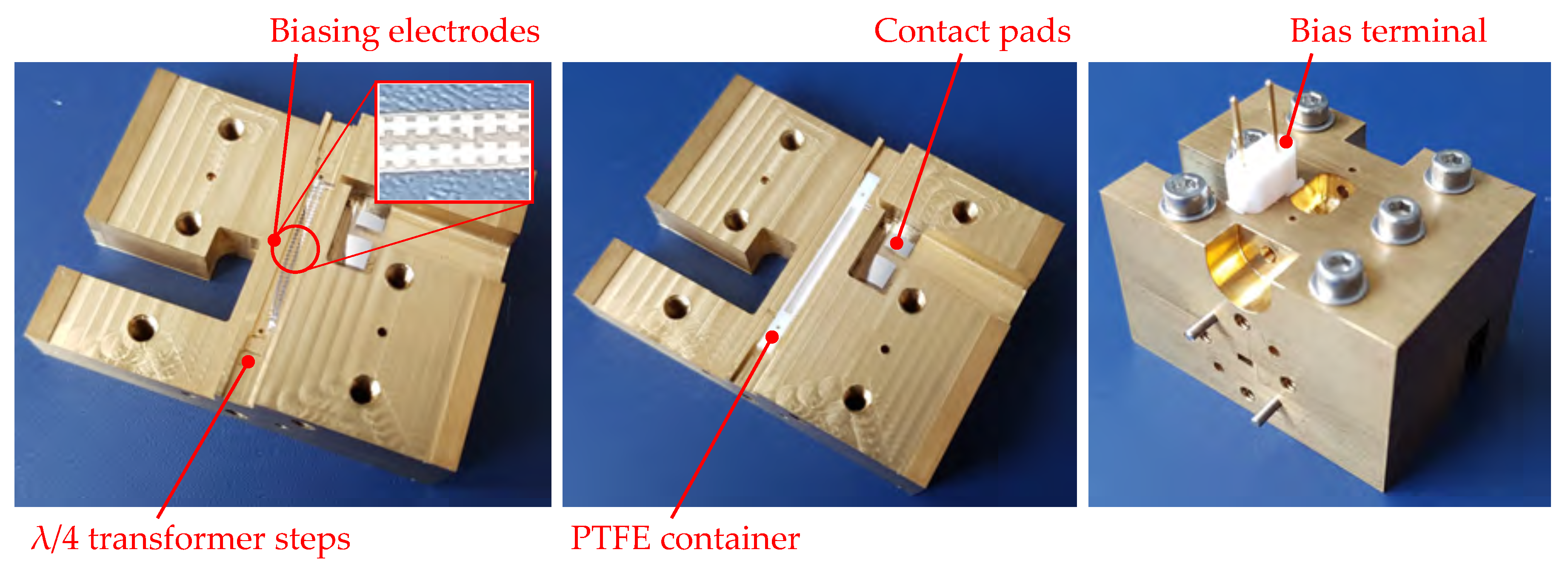
Figure 20.
Microscopic view on an evaporated as well as photolithographically processed Chromium electrode on a 20 thick PET substrate.
Figure 20.
Microscopic view on an evaporated as well as photolithographically processed Chromium electrode on a 20 thick PET substrate.

Figure 21.
Simulated S-parameter results of the electrically biased W-band metallic waveguide phase shifter.
Figure 21.
Simulated S-parameter results of the electrically biased W-band metallic waveguide phase shifter.

Figure 22.
(Left) Schematic cross-section of a DW used for the geometric approach, with . Cross-section of two common dielectric waveguide types: (Center) Step-index fiber with and (Right) Subwavelength fiber. The principle E-field distributions for both types are depicted.
Figure 22.
(Left) Schematic cross-section of a DW used for the geometric approach, with . Cross-section of two common dielectric waveguide types: (Center) Step-index fiber with and (Right) Subwavelength fiber. The principle E-field distributions for both types are depicted.

Figure 23.
Cross section of the step-index fiber phase shifter with the LC cavity highlighted in red.
Figure 23.
Cross section of the step-index fiber phase shifter with the LC cavity highlighted in red.

Figure 24.
Fabricated phase shifter and measurement setup of the step-index phase shifter. Two of four electrodes are removed to enable a view of the LC core.
Figure 24.
Fabricated phase shifter and measurement setup of the step-index phase shifter. Two of four electrodes are removed to enable a view of the LC core.
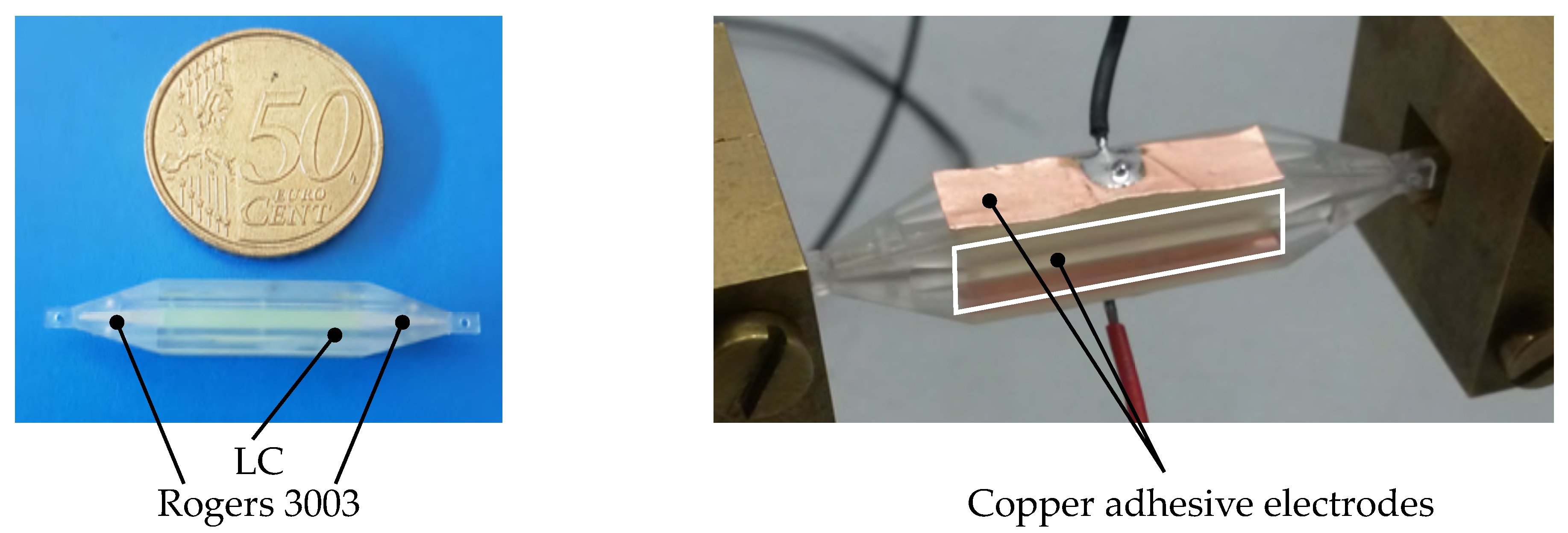
Figure 25.
Measured (solid) and simulated (dashed) results of the step-index phase shifter. For simplification, S-parameter plots show perpendicular orientation only.
Figure 25.
Measured (solid) and simulated (dashed) results of the step-index phase shifter. For simplification, S-parameter plots show perpendicular orientation only.

Figure 26.
Cross-section of the phase shifter designed as subwavelength fiber as presented in [43].
Figure 26.
Cross-section of the phase shifter designed as subwavelength fiber as presented in [43].

Figure 27.
Measurement setup of the subwavelength fiber phase shifter.

Figure 28.
Measured (solid) and simulated (dashed) results of the subwavelength fiber phase shifter. For simplification, S-parameter plots show perpendicular orientation only.
Figure 28.
Measured (solid) and simulated (dashed) results of the subwavelength fiber phase shifter. For simplification, S-parameter plots show perpendicular orientation only.

Figure 29.
Fully dielectric antenna array presented in [44]. (Left) It consists of four rod antennas which are fed by a multimode interference power divider; (Right) Further development could be the integration of the subwavelength fiber phase shifter.
Figure 29.
Fully dielectric antenna array presented in [44]. (Left) It consists of four rod antennas which are fed by a multimode interference power divider; (Right) Further development could be the integration of the subwavelength fiber phase shifter.

Figure 30.
Field plot of the fully dielectric antenna array.

Table 1.
Summary of combination of different alignment mechanism and their application to tunable microwave devices. Note that the numbering of the states has been arbitrarily chosen. “Not tunable” denotes combinations where electrical tuning cannot be achieved. E.g., a surface-surface combination will result in a static configuration. “Not used” denotes combinations, which can be used in principle but are not used in practice.

Table 2.
Material properties of different LC mixtures at room temperature.
| LC Mixture | 19 GHz | 1 kHz | |||||||
|---|---|---|---|---|---|---|---|---|---|
| (%) | (C) | (mPa s) | |||||||
| E7 | 2.98 | 0.009 | 2.53 | 0.022 | 15 | 19.6 | 5.2 | 58 | 252 |
| BL111 | 3.25 | 0.0084 | 2.64 | 0.0218 | 18.77 | 22.0 | 5.5 | 85 | 283 |
| CLHS-1 | 3.2 | 0.0033 | 2.46 | 0.0131 | 23.1 | ||||
| GT3-23001 | 3.28 | 0.0038 | 2.46 | 0.0143 | 25.2 | 8.0 | 4.0 | 173.5 | 727 |
| GT5-26001 | 3.27 | 0.0022 | 2.39 | 0.007 | 27 | 3.7 | 2.7 | 146 | 1958 |
| GT5-28004 | 3.32 | 0.0014 | 2.4 | 0.0043 | 27.7 | 3.5 | 2.7 | 151 | 5953 |
Table 3.
Comparison of different phase shifter technologies at W-band.
| Technology | Implementation | f | IL | FoM | REF | |
|---|---|---|---|---|---|---|
| (GHz) | () | (dB) | (/dB) | |||
| GaN | 2-bit RTPS | 80 | 82.5 | 3.7 | 17 | [47] |
| MEMS | 4-bit loaded line | 60 | 250 | 3 | 83 | [48] |
| Waveguide MEMS | 106 | 47 | 3.4 | 13 | [49] | |
| 3-bit switched line | 77 | 315 | 5.7 | 55 | [45] | |
| MEMS & CMOS | RTPS (CMOS ) | 65 | 144 | 3.2 | 42 | [50] |
| LC | Ridged waveguide | 96 | 500 | 7.2 | 70 | [51] |
| Metallic waveguide (magnetic bias) | 100 | 309 | 2.3 | 135 | [39] | |
| Subwavelength fiber | 103 | 140 | 2.3 | 60 | [43] | |
| Step-index fiber | 103 | 390 | 3.9 | 100 | [42] | |
| LC & MEMS | Loaded line | 93 | 190 | 4.5 | 42 | [52] |
© 2018 by the authors. Licensee MDPI, Basel, Switzerland. This article is an open access article distributed under the terms and conditions of the Creative Commons Attribution (CC BY) license (http://creativecommons.org/licenses/by/4.0/).
Share and Cite
MDPI and ACS Style
Maune, H.; Jost, M.; Reese, R.; Polat, E.; Nickel, M.; Jakoby, R. Microwave Liquid Crystal Technology. Crystals 2018, 8, 355. https://doi.org/10.3390/cryst8090355
AMA Style
Maune H, Jost M, Reese R, Polat E, Nickel M, Jakoby R. Microwave Liquid Crystal Technology. Crystals. 2018; 8(9):355. https://doi.org/10.3390/cryst8090355
Chicago/Turabian StyleMaune, Holger, Matthias Jost, Roland Reese, Ersin Polat, Matthias Nickel, and Rolf Jakoby. 2018. "Microwave Liquid Crystal Technology" Crystals 8, no. 9: 355. https://doi.org/10.3390/cryst8090355
Note that from the first issue of 2016, this journal uses article numbers instead of page numbers. See further details here.