Article

Analysis of Waveguides on Lithium Niobate Thin Films

School of Physics, State Key Laboratory of Crystal Materials, Shandong University, Jinan 250100, China
*
Author to whom correspondence should be addressed.
Crystals 2018, 8(5), 191; https://doi.org/10.3390/cryst8050191
Submission received: 5 April 2018 / Revised: 24 April 2018 / Accepted: 24 April 2018 / Published: 27 April 2018

Abstract

:
Waveguides formed by etching, proton-exchange (PE), and strip-loaded on single-crystal lithium niobate (LN) thin film were designed and simulated by a full-vectorial finite difference method. The single-mode condition, optical power distribution, and bending loss of these kinds of waveguides were studied and compared systematically. For the PE waveguide, the optical power distributed in LN layer had negligible change with the increase of PE thickness. For the strip-loaded waveguide, the relationships between optical power distribution in LN layer and waveguide thickness were different for quasi-TE (q-TE) and quasi-TM (q-TM) modes. The bending loss would decrease with the increase of bending radius. There was a bending loss caused by the electromagnetic field leakage when the neff of q-TM waveguide was smaller than that of nearby TE planar waveguide. LN ridge waveguides possessed a low bending loss even at a relatively small bending radius. This study is helpful for the understanding of waveguide structures as well as for the optimization and the fabrication of high-density integrated optical components.

1. Introduction

Lithium niobate (LN) is one of the best known ferroelectric crystals gifted with many advantages—such as excellent electro-optic, nonlinear-optic, acousto-optic, piezoelectric, and pyroelectric properties—which makes it an attractive material for photonic, electronic, and sensor applications [1,2]. In recent years, high-refractive-index contrast, single-crystal LN thin film on a low refractive index SiO2 cladding layer (lithium niobate on insulator, LNOI) or other substrates, has been fabricated using ion implantation and wafer bonding technologies [3,4]. The high-refractive-index contrast between LN and SiO2, enabling good confinement and strong guiding of light, and a high-density photonic integrated circuit is expected. Various photonic devices based on LN thin films have been reported, such as photonic crystals [5,6,7], electro-optical modulators [8,9,10,11], wavelength conversion devices [12,13,14,15], and heterogeneous LN photonic devices [16,17,18].
Waveguides are fundamental elements that can form various devices of an optical integrated circuit. Nano-scale waveguides in LNOI is essential for photonic integrated circuits with low power consumption and high integration density. Many methods have been reported to fabricate waveguides with good performance on LN thin film, including dry etching [19,20], proton-exchange (PE) [21], and strip-loaded [22]. The transmission losses of LN ridge waveguides fabricated via dry etching were reported to be 0.027, 0.3, and 0.4 dB/cm, respectively [19,20,23]. The losses of the PE waveguides were 0.2 and 0.6 dB/cm, respectively [21,24]. Various materials were used as loading strip to fabricate strip-loaded waveguides. For example, SiN strip-loaded waveguides presented the transmission losses of 0.3, 1, and 7 dB/cm, respectively [14,25,26]. The transmission losses of Si strip-loaded waveguides were 0.8, 1.3, and 6 dB/cm, respectively [18,27,28]. Bent waveguide is a basic building block for many integrated optical devices, such as Y-junctions, optical delay lines, resonators, and interferometers [29,30,31]. Small bending radius is preferred to reduce the dimensions of the photonic devices. Low bending loss is important to low power consumption devices. In this paper, LN ridge, PE, and strip-loaded waveguides have been analyzed and compared. Waveguide simulations based on full-vectorial finite difference method were performed by varying the geometrical parameters of different waveguide configurations to investigate the single-mode condition, optical power distribution in the straight waveguides, and bending loss of the bent waveguides. The different variation trends in optical power distribution in LN layer between q-TE and q-TM modes were explained. The mechanisms of leakage loss in TM polarization were studied.

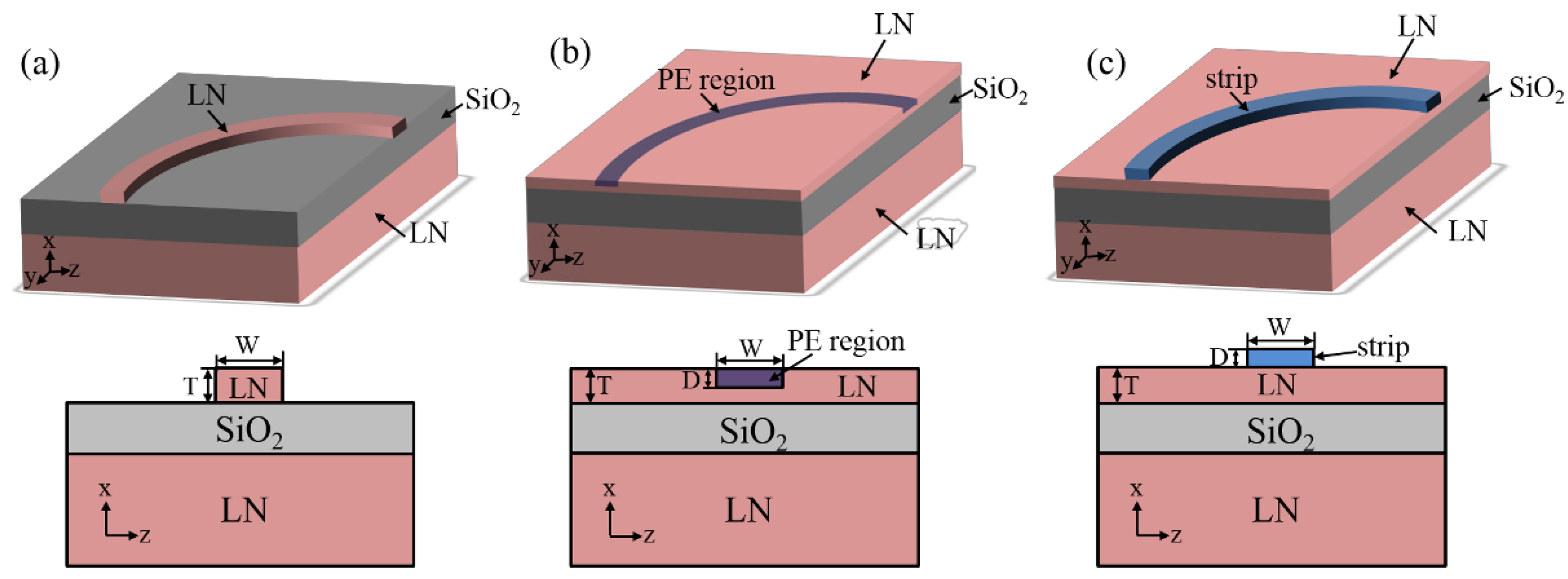
2. Design of Waveguide Geometry

Three different configurations—including ridge waveguides, PE waveguides, and strip-loaded waveguides on LN thin film—were discussed. Figure 1a shows the schematic and cross-section of an LN ridge bent waveguide. From the bottom to the top, there are the LN substrate, SiO2 cladding layer, and LN ridge. Figure 1b shows the schematic and cross-section of an LN PE bent waveguide. The PE region is embedded in LN thin film. Since the lateral diffusion could be ignored when the exchanged depth was much smaller than the waveguide width and the exchange process results in step-like index profiles, the designed PE region was set as a rectangle. Figure 1c shows the schematic and cross-section of a strip-loaded bent waveguide, which could be regarded as a combination of the LN planar waveguide and a superincumbent strip. The refractive index of the strip material was larger than 1, which could effectively define the waveguide path [32]. Here in, four materials (SiO2, SiN, TiO2, and Si) which were commonly used as loading strip of LN planar waveguide were simulated and discussed.
Many numerical methods have been used in the simulation of waveguides [33,34]. Among them, the full-vectorial finite difference method is regarded as a simple and effective method to solve the mode profile and bending loss. The mechanism of this method is shown as follows. The finite difference algorithm is used for meshing the waveguide geometry, and has the ability to accommodate arbitrary waveguide structure. Once the structure is meshed, Maxwell’s equations are then formulated into a matrix eigenvalue problem and solved using sparse matrix techniques to obtain the effective index and mode profiles of the waveguide modes. Perfectly matched layer (PML) boundary conditions could absorb electromagnetic energy incident upon them, allowing radiation to propagate out of the computational area without interfering with the field inside. This boundary condition could benefit the bending loss calculation [35]. The telecommunication wavelength of 1.55 µm was used in all the following simulations. The LNOI were all x-cut, and the birefringence of the LN material was considered in the simulations. The ordinary and extraordinary refractive indices of the LN thin film at wavelength 1.55 µm were set to be 2.211 and 2.138, respectively, according to the Sellmeier equation [36]. The ordinary and extraordinary refractive indices of the PE region in LN thin film at wavelength 1.55 µm were 2.161 and 2.218, respectively, which were obtained according to [21]. The refractive indices of SiO2 [37], SiN [25], TiO2 [38], and Si [22] at wavelength 1550 nm were 1.46, 1.9, 2.3, and 3.48, respectively.

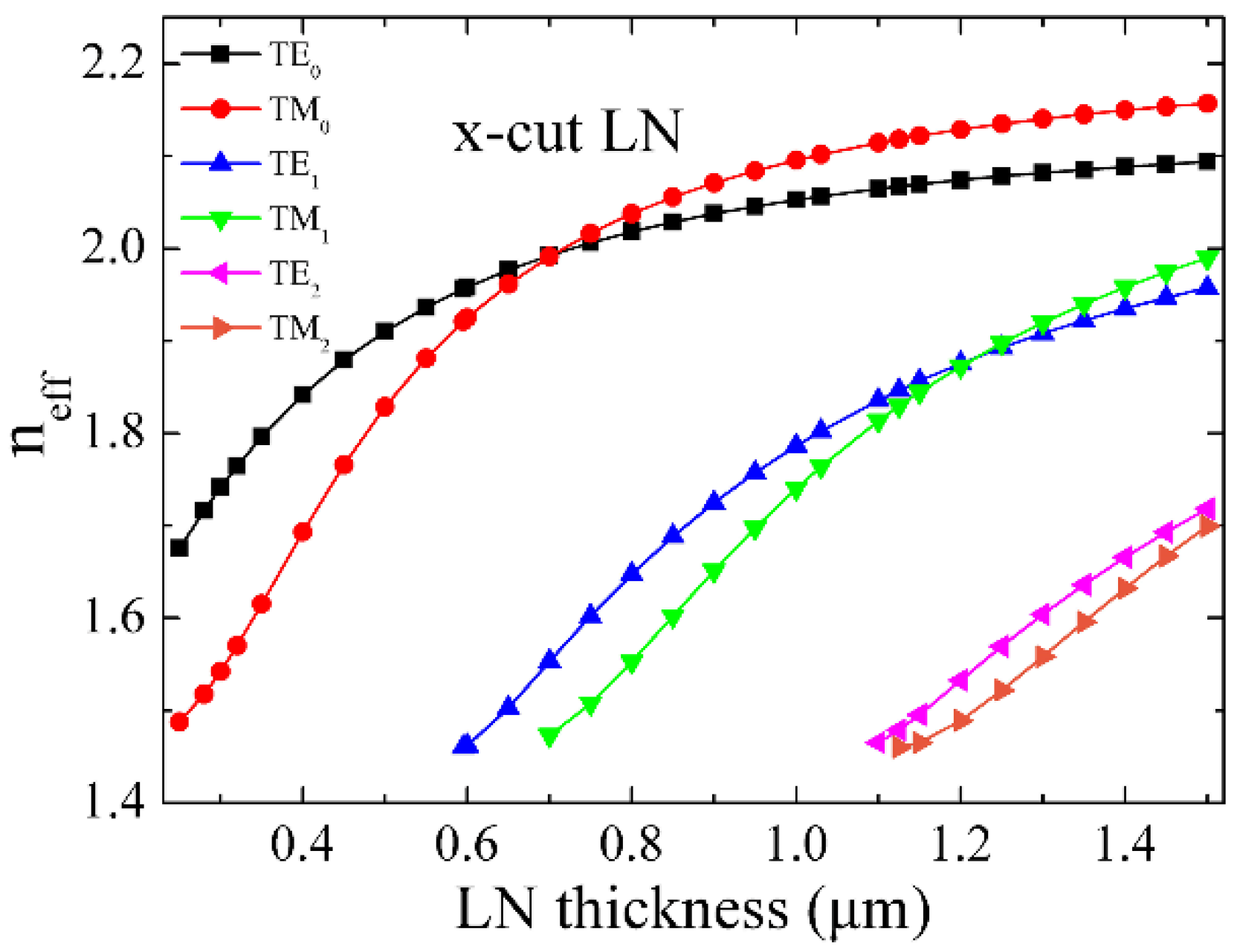
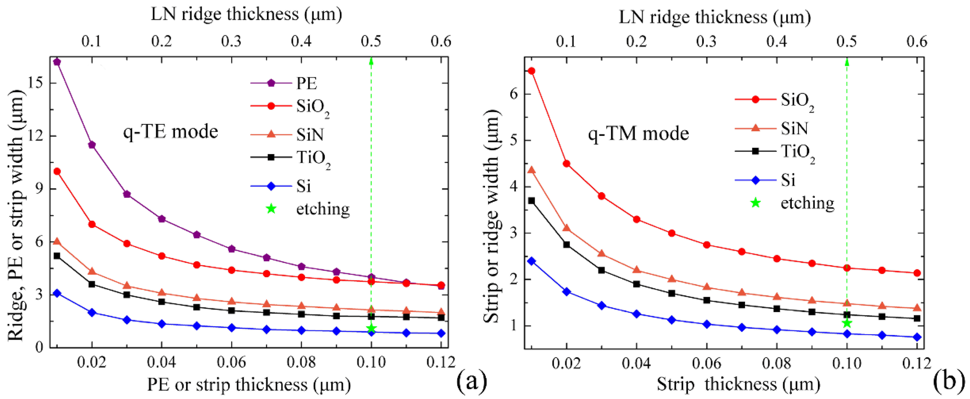
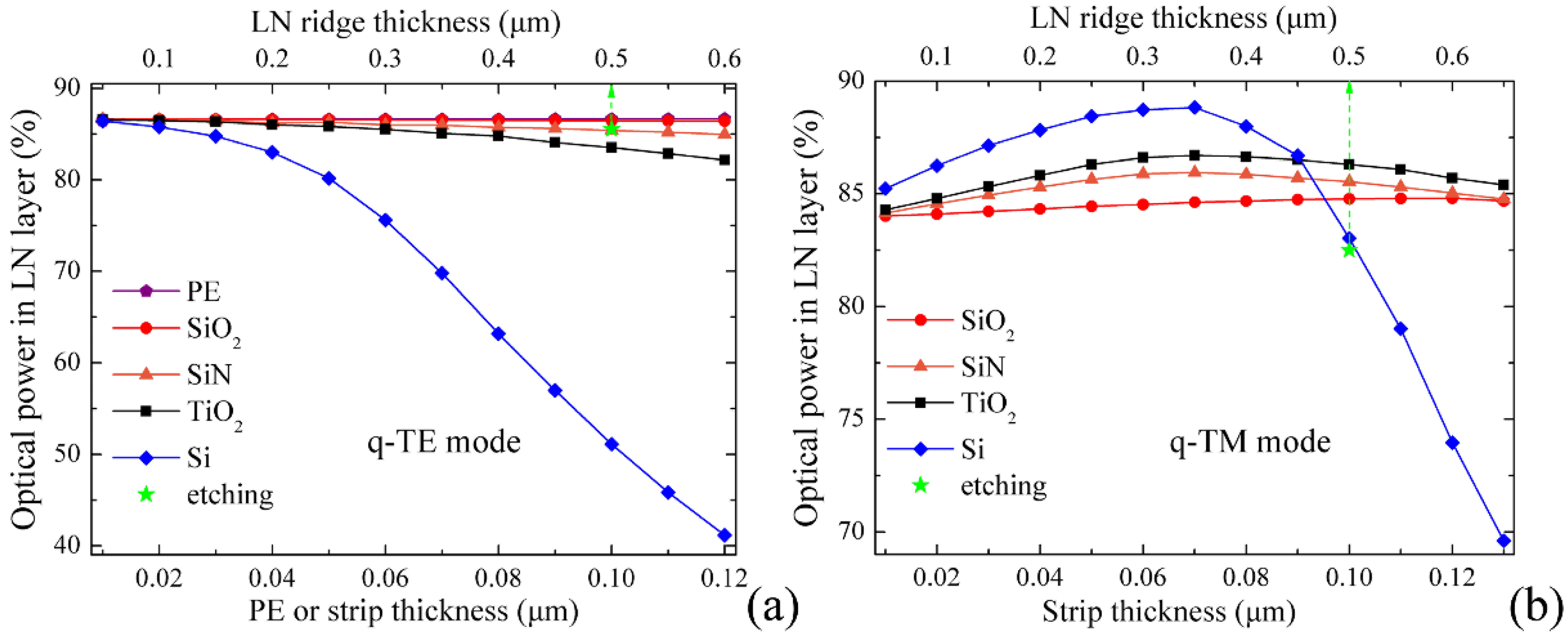
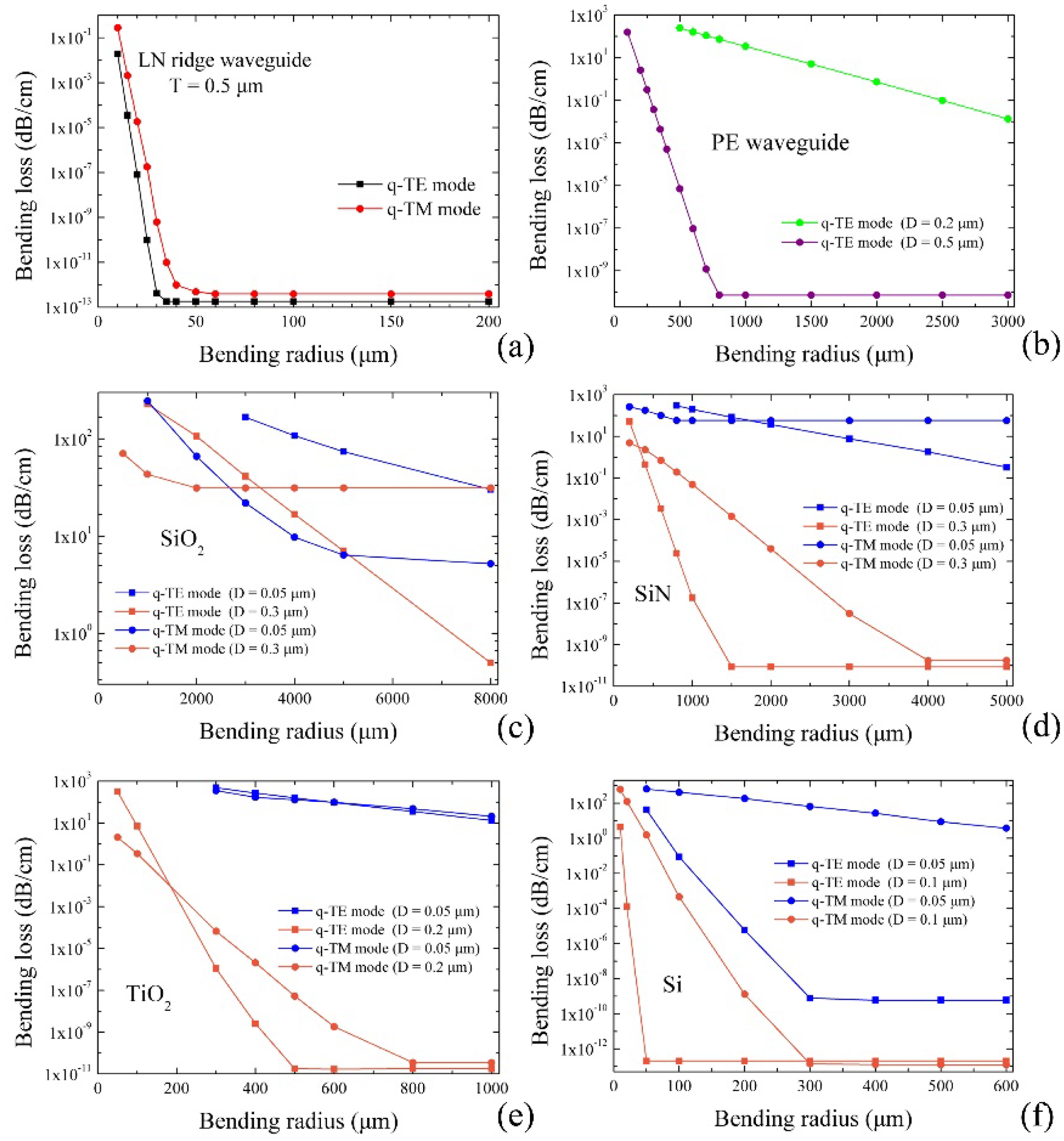
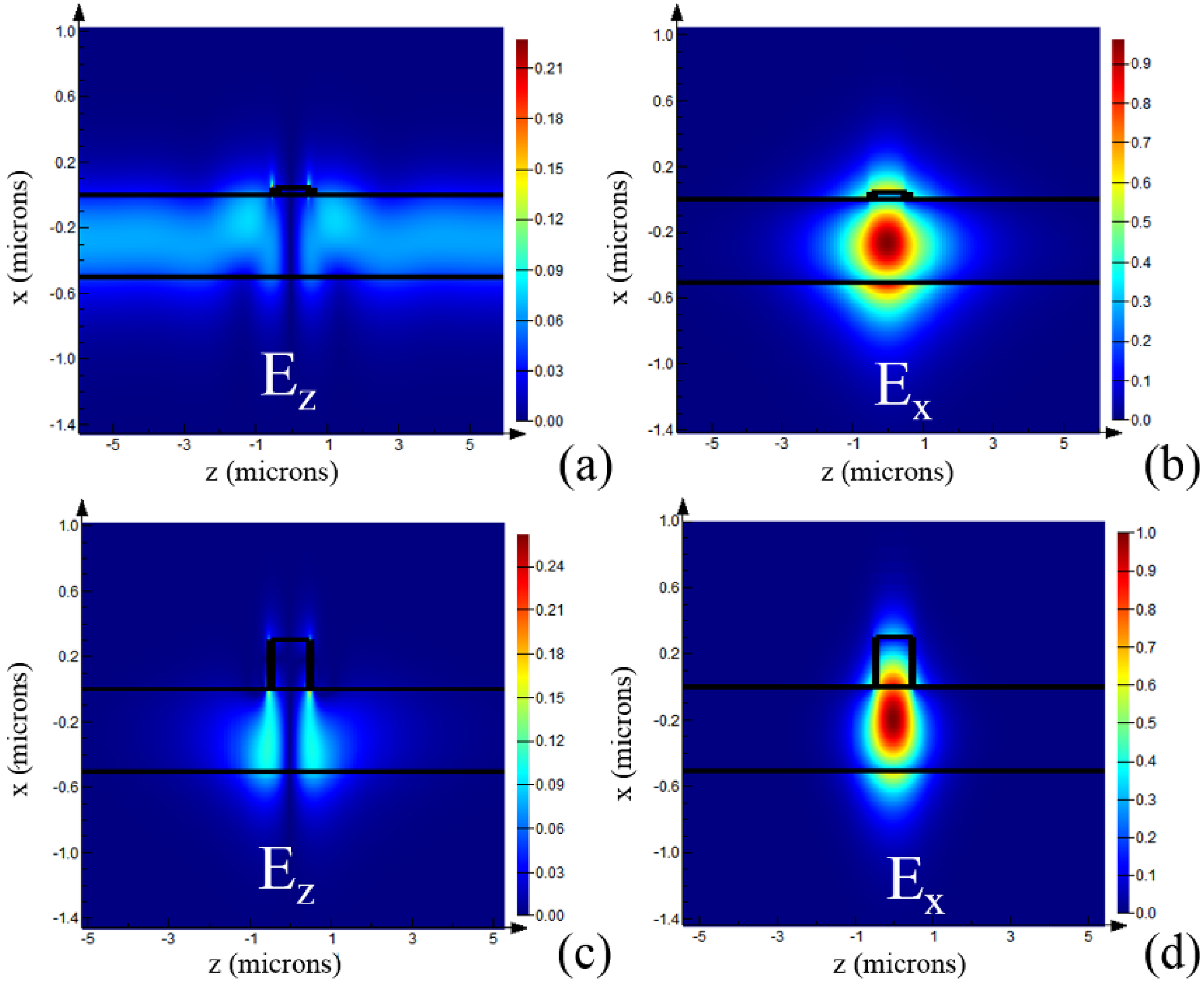
3. Results and Discussion

In order to discuss how light is confined and guided in different waveguide geometries, the parameters of the waveguides (the thickness T of the LN layer, the thickness D and width W of the PE region and loading strip, and the thickness T and width W of ridge waveguide) were used in the simulation. The single mode condition has been firstly simulated. Figure 2 shows the relationship between the LN thin film thickness and the number of mode that could be supported in LN planar waveguide. The first order mode of the TE and TM modes appeared at the LN thickness of 0.6 μm and 0.7 μm, respectively. To ensure that only one electric field intensity peak is supported in the vertical direction of the LN thin film, the thickness of LN should be less than this critical value. In the following simulation, the thickness of LN was all selected as 0.5 μm. Figure 3 shows the single-mode condition in the ridge and channel waveguides. The curves show the boundary between the single-mode and multi-mode conditions. The waveguide dimensions beneath the curves fulfilled the single mode condition. For the LN ridge waveguide, the single mode condition of the quasi-TE (q-TE) mode and quasi-TM (q-TM) mode were 1.1 μm and 1.06 μm, respectively (see the green star, the thickness of LN ridge was fixed at 0.5 μm). PE process only increased the extraordinary refractive index of the crystal. Therefore, only q-TE mode was supported in the x-cut PE waveguides. As shown in Figure 3a, as the PE thickness (D) increased, the PE width (W) should decrease in order to fulfill the single-mode condition. For the strip-loaded waveguide, the strip width (W) also decreased with the increase of strip thickness (D) for both q-TE and q-TM modes. The strip width for the single-mode condition would increase for the lower refractive index material at the same strip thickness. In the following simulation, the widths of LN ridge, PE region, and loading strip were all selected as 1 μm to ensure that only one mode was supported in LN thin film.
The optical power in LN layer was defined as the ratio of the optical power in the LN region to the total optical power of all the space. Consequently, the value was between 0 and 1. As shown in Figure 4a, the optical power of the q-TE mode in the LN ridge was 85.6% (see the green star, the thickness and width of LN ridge were fixed at 0.5 μm and 1 μm, respectively). For the PE waveguide, the optical power of the q-TE mode showed a very slight increase with the increase of PE thickness. The reason was that the light confinement by refractive index contrast increased with the increase of the PE thickness as well as the neff of the PE waveguide. For the strip-loaded waveguide, the optical power of the q-TE mode in the LN layer decreased slightly as the strip thickness increased, expect for Si strip, which decreased obviously with the increase of Si thickness. This indicated that the refractive index of strip had some influence on the distribution of the optical power. With the increase of the refractive index of the strip, the optical power confined in LN layer would gradually be attracted into the strip. As shown in Figure 4b, the optical power of the q-TM mode in the LN ridge was 82.5%. For the strip-loaded waveguide, the optical power of the q-TM mode in the LN layer initially increased as the trip thickness increased. The maximum value was obtained at a thickness of approximately 0.12, 0.07, 0.07, and 0.07 μm for the SiO2, SiN, TiO2, and Si strip, respectively. As the strip thickness increased further, the optical power in the LN layer decreased. The reason could be explained as follows. Firstly, the strip thickness is too thin to effectively confine the optical power in LN layer, and a small part of optical power could leak into the SiO2 buffer layer. With the increase of strip thickness, the light confinement by the loading strip increases. The optical power in the LN layer begins decrease when the optical power is gradually attracted into the strip.
A bent waveguide which possesses both a small bending radius and a low bending loss is preferred. Figure 5a shows the relationship between the bending loss and the bending radius of a LN ridge waveguide. The thickness and width of LN ridge were fixed as 0.5 and 1 μm, respectively. The bending loss decreased sharply with the increase of bending radius. The minimal bending radii having low bending losses (10−5 dB/cm, for example) were 15 and 20 μm for both q-TE and q-TM modes, respectively. In the experiment, a microring resonator with a bending loss of 0.1 dB/cm at a bending radius of 80 μm was realized [19]. The relationship between the bending loss and the bending radius of PE waveguide with different PE depths is shown in Figure 5b. With the increase of bending radius, the bending loss decreased. The thickness of PE region had an obvious influence on bending loss. When D = 0.2 μm, the bending loss was 34 dB/cm at radius of 1 mm, while the bending loss was 10−11 dB/cm when D = 0.5 μm with the same radius. The increase of PE thickness could cause the increase of neff of waveguide, so that the light confinement of the waveguide increased, and the bending loss decreased correspondingly. The Y-junctions based on PE waveguide with 4–8 mm bending radii were designed and fabricated and a stable splitting ratio of 1:1 was obtained [21]. Figure 5c–f shows the relationship between the bending loss and the bending radius as well as strip thickness (D) of the strip-loaded waveguides with four different loading strip materials, respectively. The widths of strips were fixed as 1 μm for all the waveguides. The bending loss decreased with the increase of bending radius for both q-TE and q-TM modes. The refractive index of loading strip had a remarkable influence on bending loss. A higher refractive index would cause a lower bending loss. For q-TE mode, a low bending loss (10−5 dB/cm, for example) could be obtained if the bending radius was large enough. The LN thin film Mach–Zehnder modulator with SiN strip-loaded waveguide has been reported, which demonstrated a Vπ·L of 3 V cm and a 3-dB bandwidth of 8 GHz [26]. While for q-TM mode, there is another loss mechanism. The electric field Ez (coordinate direction is shown in Figure 1) in the q-TM mode would cause leakage loss when the neff of the strip-loaded waveguide was smaller than that of nearby LN planar waveguide in TE polarization [39]. Take the SiN strip-loaded bent waveguide as an example, as shown in Figure 5d, when the thickness of SiN strip was 0.05 μm, the neff of the SiN strip-loaded waveguide (nTM00 = 1.844) was smaller than that of nearby LN planar waveguide (nTE0 = 1.910), and the electric field Ez in the strip-loaded waveguide mode would excite the TE mode in the planar waveguides on both sides of the strip-loaded waveguide, causing waveguide loss. In this case, the minimum loss is 57 dB/cm. Figure 6a,b show the Ez and Ex distributions with a strip thickness of 0.05 μm. Figure 6a shows there was electric field outside the strip-loaded waveguide region, indicating an optical power leakage. When the thickness of SiN strip was 0.3 μm, the neff of the SiN strip-loaded waveguide (nTM00 = 1.922) was larger than that of nearby LN planar waveguide (nTE0 = 1.910), the Ez component could not excite the waveguide mode in the planar waveguides besides the strip-loaded waveguide. The bending loss could be very small (around 10−10 dB/cm at radius of 4 mm). Figure 6c,d show the Ez and Ex distributions with a strip thickness of 0.3 μm. There was almost no electric field outside the strip-loaded waveguide region, indicating negligible optical power leakage. This kind of leakage loss mechanism caused by TE↔TM mode coupling could be found in straight waveguides [21].

4. Conclusions

In conclusion, a full-vectorial finite difference method was used to simulate various waveguides—including ridge waveguide, PE waveguide, and strip-loaded waveguides—in single-crystal LN thin film. Single mode conditions were obtained. The optical power percentage in LN layer was calculated. For q-TE mode, the optical power in the etched LN ridge waveguide was 85.6% when the waveguide width was 1 μm and the LN thickness was 0.5 μm. The optical power in the PE waveguide showed slight increase with the increase of PE thickness, while the optical power decreased with the increase of strip thickness. For q-TM mode, the optical power in the etched LN ridge waveguide was 82.5%. The optical power in the strip-loaded waveguide initially increased as the strip thickness increased. The maximum value was obtained at the thickness of approximately 0.12, 0.07, 0.07, and 0.07 μm for the SiO2, SiN, TiO2, and Si strip, respectively. As the strip thickness increased further, the optical power in the LN layer decreased. The bending loss decreased with the increase of bending radius. For the LN ridge waveguide, the minimal bending radii (with bending loss of 10−5 dB/cm, for example) were 15 and 20 μm for q-TE and q-TM modes, respectively. For the PE waveguide, the bending loss decreased with the increase of PE depths for q-TE mode. For the strip-loaded waveguide, a low bending loss (10−5 dB/cm, for example) could be obtained for q-TE mode if the bending radius was large enough. While for the q-TM mode, there existed an extra loss mechanism. The leakage of Ez component existed in q-TM mode when the neff of waveguide was smaller than that of the nearby planar waveguides in TE polarization. The increase of strip thickness could improve neff of waveguide to be larger than that of nearby planar waveguides, which could avoid the leakage loss. The study is useful for the fabrication of high-density integrated optical components.

Author Contributions

Hui Hu conceived the original idea; Yiwen Wang carried out the simulations, analyzed the data, and wrote the paper; Hui Hu and Zhihua Chen contributed the useful and deep discussions and modified the manuscript.

Acknowledgments

This work was supported by the National Natural Science Foundation of China (NSFC) (grants no. 61575111 and no. 11475105).

Conflicts of Interest

The authors declare no conflict of interest.

References

  1. Weis, R.S.; Gaylord, T.K. Lithium niobate: Summary of physical properties and crystal structure. Appl. Phys. A Mater. Sci. Process 1985, 37, 191–203. [Google Scholar] [CrossRef]
  2. Arizmendi, L. Photonic applications of lithium niobate crystals. Phys. Status Solidi A Appl. Res. 2004, 201, 253–283. [Google Scholar] [CrossRef]
  3. Poberaj, G.; Hu, H.; Sohler, W.; Gunter, P. Lithium niobate on insulator (LNOI) for micro-photonic devices. Laser Photonics Rev. 2012, 6, 488–503. [Google Scholar] [CrossRef]
  4. Rabiei, P.; Gunter, P. Optical and electro-optical properties of sub-micrometer lithium niobate slab waveguides prepared by crystal ion slicing and wafer bonding. Appl. Phys. Lett. 2004, 85, 4603–4605. [Google Scholar] [CrossRef]
  5. Liang, H.; Luo, R.; He, Y.; Jiang, H.; Lin, Q. High-quality lithium niobate photonic crystal nanocavities. Optica 2017, 4, 1251. [Google Scholar] [CrossRef]
  6. Kovalevich, T.; Ndao, A.; Suarez, M.; Tumenas, S.; Balevicius, Z.; Ramanavicius, A.; Baleviciute, I.; Häyrinen, M.; Roussey, M.; Kuittinen, M.; et al. Tunable Bloch surface waves in anisotropic photonic crystals based on lithium niobate thin films. Opt. Lett. 2016, 41, 5616–5619. [Google Scholar] [CrossRef] [PubMed]
  7. Lu, H.; Sadani, B.; Courjal, N.; Ulliac, G.; Smith, N.; Stenger, V.; Collet, M.; Baida, F.I.; Bernal, M.P. Enhanced electro-optical lithium niobate photonic crystal wire waveguide on a smart-cut thin film. Opt. Express 2012, 20, 2974–2981. [Google Scholar] [CrossRef] [PubMed]
  8. Rao, A.; Fathpour, S. Compact lithium niobate electrooptic modulators. IEEE J. Sel. Top. Quant. 2018, 24, 3400114. [Google Scholar] [CrossRef]
  9. Rao, A.; Patil, A.; Rabiei, P.; Honardoost, A.; DeSalvo, R.; Paolella, A.; Fathpour, S. High-performance and linear thin-film lithium niobate Mach–Zehnder modulators on silicon up to 50 GHz. Opt. Lett. 2016, 41, 5700–5703. [Google Scholar] [CrossRef] [PubMed]
  10. Cai, L.; Kang, Y.; Hu, H. Electric-optical property of the proton exchanged phase modulator in single-crystal lithium niobate thin film. Opt. Express 2016, 24, 4640–4647. [Google Scholar] [CrossRef] [PubMed]
  11. Mian, Z.; Cheng, W.; Xi, C.; Maxime, B.; Amirhassan, S.A.; Sethumadhavan, C.; Peter, W.; Marko, L. Ultra-high bandwidth integrated lithium niobate modulators with record-low Vπ. In Proceedings of the Optical Fiber Communication Conference, San Diego, CA, USA, 11–15 March 2018. [Google Scholar] [CrossRef]
  12. Wolf, R.; Breunig, I.; Zappe, H.; Buse, K. Cascaded second-order optical nonlinearities in on-chip micro rings. Opt. Express 2017, 25, 29927–29933. [Google Scholar] [CrossRef] [PubMed]
  13. Wang, C.; Li, Z.; Kim, M.; Xiong, X.; Ren, X.; Guo, G.; Yu, N.; Lončar, M. Metasurface-assisted phase-matching-free second harmonic generation in lithium niobate waveguides. Nat. Commun. 2017, 8, 2098. [Google Scholar] [CrossRef] [PubMed]
  14. Delfyett, P.; Fathpour, S. Second-harmonic generation in periodically-poled thin film lithium niobate wafer-bonded on silicon. Opt. Express 2016, 24, 29941–29947. [Google Scholar] [CrossRef]
  15. Cai, L.; Wang, Y.; Hu, H. Efficient second harmonic generation in χ(2) profile reconfigured lithium niobate thin film. Opt. Commun. 2017, 387, 405–408. [Google Scholar] [CrossRef]
  16. Rabiei, P.; Ma, J.; Khan, S.; Chiles, J.; Fathpour, S. Heterogeneous lithium niobate photonics on silicon substrates. Opt. Express 2013, 21, 25573–25581. [Google Scholar] [CrossRef] [PubMed]
  17. Chen, L.; Chen, J.; Nagy, J.; Reano, R.M. Highly linear ring modulator from hybrid silicon and lithium niobate. Opt. Express 2015, 23, 13255–13264. [Google Scholar] [CrossRef] [PubMed]
  18. Witmer, J.D.; Valery, J.A.; Arrangoiz-Arriola, P.; Sarabalis, C.J.; Hill, J.T.; Safavi-Naeini, A.H. High-Q photonic resonators and electro-optic coupling using silicon-on-lithium-niobate. Sci. Rep.-UK 2017, 7, 46313. [Google Scholar] [CrossRef] [PubMed]
  19. Zhang, M.; Wang, C.; Cheng, R.; Shams-Ansari, A.; Lončar, M. Monolithic ultra-high-Q lithium niobate microring resonator. Optica 2017, 4, 1536. [Google Scholar] [CrossRef]
  20. Krasnokutska, I.; Tambasco, J.J.; Li, X.; Peruzzo, A. Ultra-low loss photonic circuits in lithium niobate on insulator. Opt. Express 2018, 26, 897–904. [Google Scholar] [CrossRef] [PubMed]
  21. Cai, L.; Kong, R.; Wang, Y.; Hu, H. Channel waveguides and y-junctions in x-cut single-crystal lithium niobate thin film. Opt. Express 2015, 23, 29211. [Google Scholar] [CrossRef] [PubMed]
  22. Wang, Y.; Chen, Z.; Cai, L.; Jiang, Y.; Zhu, H.; Hu, H. Amorphous silicon-lithium niobate thin film strip-loaded waveguides. Opt. Mater. Express 2017, 7, 4018. [Google Scholar] [CrossRef]
  23. Siew, S.Y.; Cheung, E.J.H.; Liang, H.; Bettiol, A.; Toyoda, N.; Alshehri, B.; Dogheche, E.; Danner, A.J. Ultra-low loss ridge waveguides on lithium niobate via argon ion milling and gas clustered ion beam smoothening. Opt. Express 2018, 26, 4421–4430. [Google Scholar] [CrossRef] [PubMed]
  24. Cai, L.; Wang, Y.; Hu, H. Low-loss waveguides in a single-crystal lithium niobate thin film. Opt. Lett. 2015, 40, 3013–3016. [Google Scholar] [CrossRef] [PubMed]
  25. Chang, L.; Li, Y.; Volet, N.; Wang, L.; Peters, J.; Bowers, J.E. Thin film wavelength converters for photonic integrated circuits. Optica 2016, 3, 531. [Google Scholar] [CrossRef]
  26. Jin, S.; Xu, L.; Zhang, H.; Li, Y. LiNbO3 thin-film modulators using silicon nitride surface ridge waveguides. IEEE Photonics Technol. Lett. 2016, 28, 736–739. [Google Scholar] [CrossRef]
  27. Chen, L.; Xu, Q.; Wood, M.G.; Reano, R.M. Hybrid silicon and lithium niobate electro-optical ring modulator. Optica 2014, 1, 112. [Google Scholar] [CrossRef]
  28. Weigel, J.P.O.; Savanier, M.; DeRose, C.T.; Pomerene, A.T.; Starbuck, A.L.; Lentine, A.L.; Stenger, V.; Mookherjea, S. Lightwave circuits in lithium niobate through hybrid waveguides with silicon photonics. Sci. Rep.-UK 2016, 6, 22301. [Google Scholar] [CrossRef] [PubMed]
  29. Changlui, R.; Pinliao, Y.; Seenwang, W. Bent waveguide with a high index reflector on LiNbO3. Opt. Quant. Electron. 2000, 32, 313–325. [Google Scholar] [CrossRef]
  30. Qian, Y.; Kim, S.; Song, J.; Nordin, G.P.; Jiang, J. Efficient and compact silicon-on-insulator rib waveguide 90° bends and splitters. Opt. Mater. 2017, 72, 136–139. [Google Scholar] [CrossRef]
  31. Wang, Q.; Farrell, G.; Wang, P.; Rajan, G.; Freir, T. Design of integrated wavelength monitor based on a Y-branch with an S-bend waveguide. Sens. Actuat. A-Phys. 2007, 134, 405–409. [Google Scholar] [CrossRef]
  32. Ogusu, K.; Kawakami, S.; Nishida, S. Optical strip waveguide: An analysis. Appl. Opt. 1979, 18, 908–914. [Google Scholar] [CrossRef] [PubMed]
  33. Saitoh, E.; Kawaguchi, Y.; Saitoh, K.; Koshiba, M. TE/TM-Pass polarizer based on lithium niobate on insulator ridge waveguide. IEEE Photonics J. 2013, 5, 6600610. [Google Scholar] [CrossRef]
  34. Qiu, W.; Bernal, M.P.; Ndao, A.; Guyot, C.; Hameed, N.M.; Courjal, N.; Maillotte, H.; Baida, F.I. Analysis of ultra-compact waveguide modes in thin film lithium niobate. Appl. Phys. B 2015, 118, 261–267. [Google Scholar] [CrossRef]
  35. Lumerical Solutions. Available online: http://www.lumerical.com/ (accessed on 5 April 2018).
  36. Zelmon, D.E.; Small, D.L. Infrared corrected Sellmeier coefficients for congruently grown lithium niobate and 5 mol. % magnesium oxide-doped lithium niobate. J. Soc. Am. B 1997, 14, 3319–3332. [Google Scholar] [CrossRef]
  37. Landsberger, L.M.; Tiller, W.A. Refractive index, relaxation times and the viscoelastic model in dry-grown SiO2 films on Si. Appl. Phys. Lett. 1987, 51, 1416–1418. [Google Scholar] [CrossRef]
  38. Li, S.; Cai, L.; Wang, Y.; Jiang, Y.; Hu, H. Waveguides consisting of single-crystal lithium niobate thin film and oxidized titanium stripe. Opt. Express 2015, 23, 24212–24219. [Google Scholar] [CrossRef] [PubMed]
  39. Ogusu, K.; Tanaka, I. Optical strip waveguide: An experiment. Appl. Opt. 1980, 19, 3322–3325. [Google Scholar] [CrossRef] [PubMed]
Figure 1. Schematic and cross-section of the (a) LN ridge bent waveguide, (b) PE bent waveguide, and (c) strip-loaded bent waveguide.
Crystals 08 00191 g001
Figure 2. Relationship between the LN thin film thickness and the number of modes that can be supported in LN planar waveguide at a wavelength of 1550 nm.
Crystals 08 00191 g002
Figure 3. Single-mode conditions of LN ridge waveguides, PE waveguides and strip-loaded waveguides for the (a) q-TE and (b) q-TM mode at a wavelength of 1550 nm.
Crystals 08 00191 g003
Figure 4. Optical power confined in LN layer for the (a) q-TE and (b) q-TM mode.
Crystals 08 00191 g004
Figure 5. Bending losses of LN (a) ridge waveguide, (b) PE waveguide, and (cf) four kinds of strip-loaded waveguides for the q-TE and q-TM modes.
Crystals 08 00191 g005
Figure 6. Ez and Ex components of SiN strip-loaded waveguides with a 1 μm strip width and 0.05 μm strip thickness (a,b), and a 1 μm strip width and 0.3 μm strip thickness (c,d) for the q-TM mode.
Crystals 08 00191 g006

