1. Introduction
In recent years, the laser-nanostructure interaction has become of great interest due to the application of NPs in different fields, such as nano-optics and nano-electronics [
1,
2,
3,
4], laser nano-biomedicine [
5,
6,
7,
8] and catalysis [
9,
10]. This is due to the well-known property of metallic NPs called localized surface plasmon resonance (LSPR), in which the conduction band electrons oscillate coherently with the electric field of the incident light. The frequency and intensity of the LSPR absorption bands are characteristic of the material (gold, silver or platinum) and are highly sensitive to the size, distribution, and shape of the nanostructures, as well as to the environments which surround them [
11,
12].
Optical excitation and non-radiative relaxation of the LSPR create a photo-thermal effect due to the conversion of light energy into heat. Within this LSPR-mediated heating process, the light absorbed by the nanoparticle generates a non-equilibrium electron distribution that decays via electron-electron scattering. The hot electron gas equilibrates with lattice phonons which transfer this energy into the surrounding medium, resulting in a local temperature increase [
13]. The total energy transfer process is rapid (10
−10–10
−12 s) and efficient [
14].
This effect, renamed the photo-thermal effect in plasmonic nanoparticles, has already found applications in cancer therapy [
15,
16], optofluidic control [
17], nano-welding [
18], optical data storage [
19], imaging [
20] and sensing [
21].
Recent advances in both bottom-up and top-down fabrication techniques offer a tremendous variety of metallic NPs with numerous geometries [
22] which can be immobilized on a flat substrate with a resolution down to a few tens of nanometers. These substrates, if appropriately designed, can be used as thermo-smart platforms, able to generate a desired value of temperature by controlling the number of GNPs photo-excited at the same time.
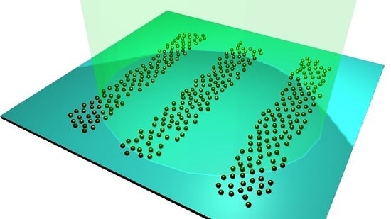
In the field of additive manufacturing, two-photon direct laser writing (2P-DLW) represents the most advanced optical technique for the fabrication of 2D and 3D arbitrary structures, with resolutions well below the diffraction limit [
23]. Focusing a femto-second infrared laser (λ = 780 nm, pulse duration of 100 femtosecond (fs) on a polymeric matrix doped with a photosensitive metal precursor, it is possible to create NPs inside the focus figure (“voxel” in a volume) through the photo-reduction of the metallic element in the precursor.
The
nanoparticles were formed by the direct photo-reduction of Au
, according to the mechanism reported in References [
24,
25]. Briefly, during the irradiation process, the excited
forms the caged
complex (Equations (1) and (2)). This complex then dissociates (Equation (3)) and the unstable
quickly disproportionates to form
and
(Equation (4)).
absorbs another photon to form
(Equation (5)).
associates to form nuclei and the AuNPs (Equation (6)):
While the process of photo-reduction of a silver precursor (e.g., AgNO
3) leads to the oxidation of the polymeric matrix, the photo-reduction of HAuCl
4 does not chemically change the matrix. The photo-reduction of GNPs, in fact, is not promoted by the oxidation of the PVA [
24].
Recent studies demonstrated the possibility to create stripes at the submicron scale, rich in gold nanoparticles, in a poly-vinyl alcohol (PVA) matrix doped with HAuCl
4, by means of this 2P-DLW technique [
26].
In the present study, we realized four different samples of GNP stripes spaced by 0.5, 2, 10 and 100 µm. The thermal response of each sample, characterized by a different grating periodicity of GNPs, was monitored by means of a thermographic camera as a function of the impinging intensity of a continuous beam laser (λ = 532 nm). In this way, a careful analysis of the macroscopic photo-induced heat generation of this particular 1D arrangement of GNPs was carried out.
2. Results and Discussions
A surface of 1 mm
2 of a glass substrate was structured with a mono-dimensional grating of GNPs, direct laser–written in dried films of PVA and HAuCl
4. According to the procedure described in Reference [
27], the samples were developed in H
2O to remove all the unexposed material, leaving only the stripes of GNPs sticking to the glass substrate.
The width of each GNP stripe, obtained by using a laser power of 25 mW and a scanning speed of 200 µm/s, was of the order of 1.5 µm. Then we decided to design four gratings with different periods in order to control the number of GNPs that were excited at the same time by the resonant radiation; in particular, we chose a periodicity between the stripes of 0.5, 2, 10 and 100 µm. The four samples were first analyzed by means of an optical microscope and then by an atomic force microscope (AFM).
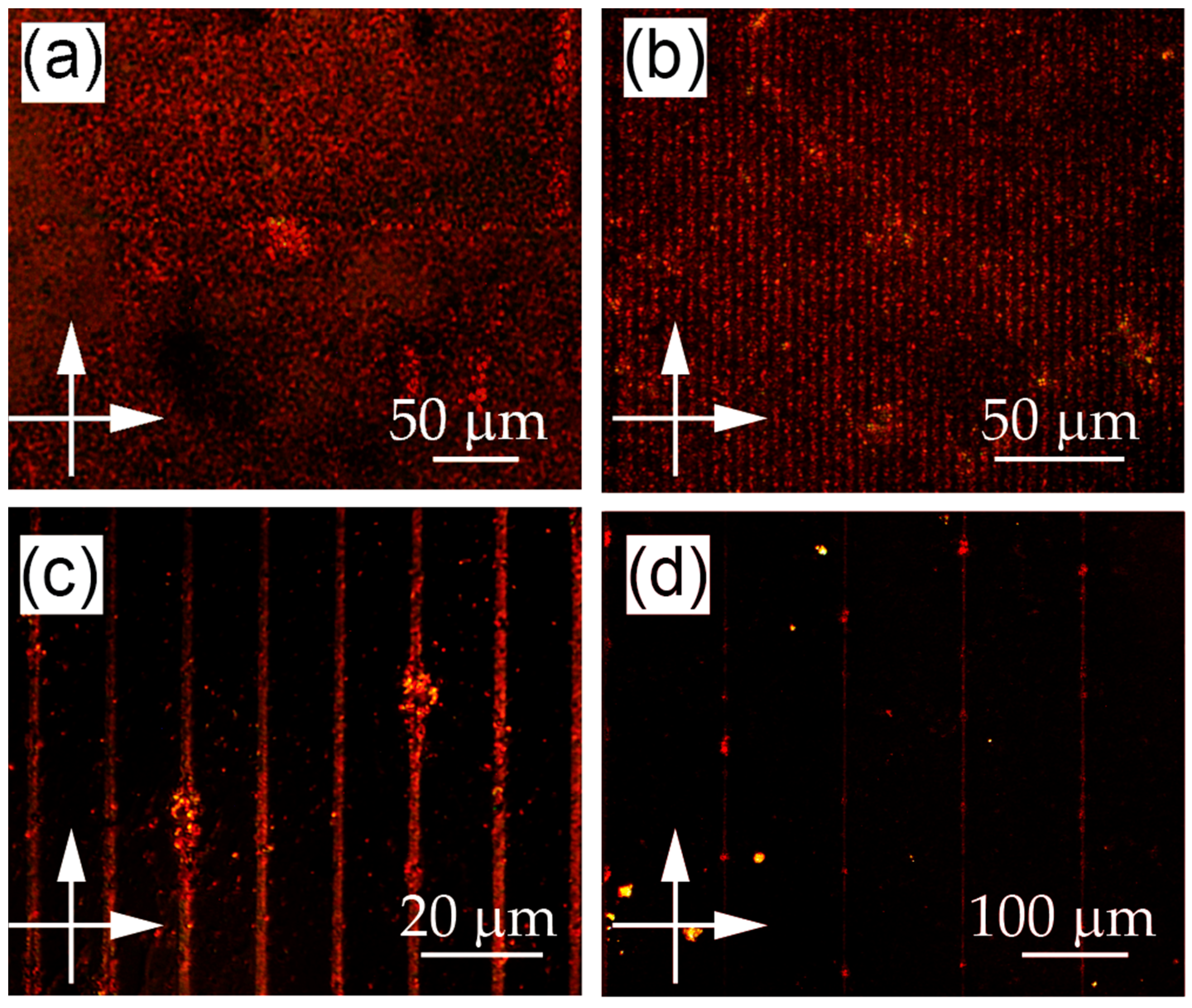
Optical images were acquired through a 50× and 100× objective, between crossed polarizers, which allow evidencing the macroscopic response of gold nanoparticles and identifying the different gratings due to scattering effects (
Figure 1). The sample with the period of 0.5 µm, in
Figure 1a, appears as a dense square of GNPs, which does not show any pattern inside. On the other hand, the grating structure is evident in the samples with the other designed periods; thus, we obtained stripes rich in GNPs, spaced from 0.5 µm (
Figure 1b) to 100 µm (
Figure 1d).
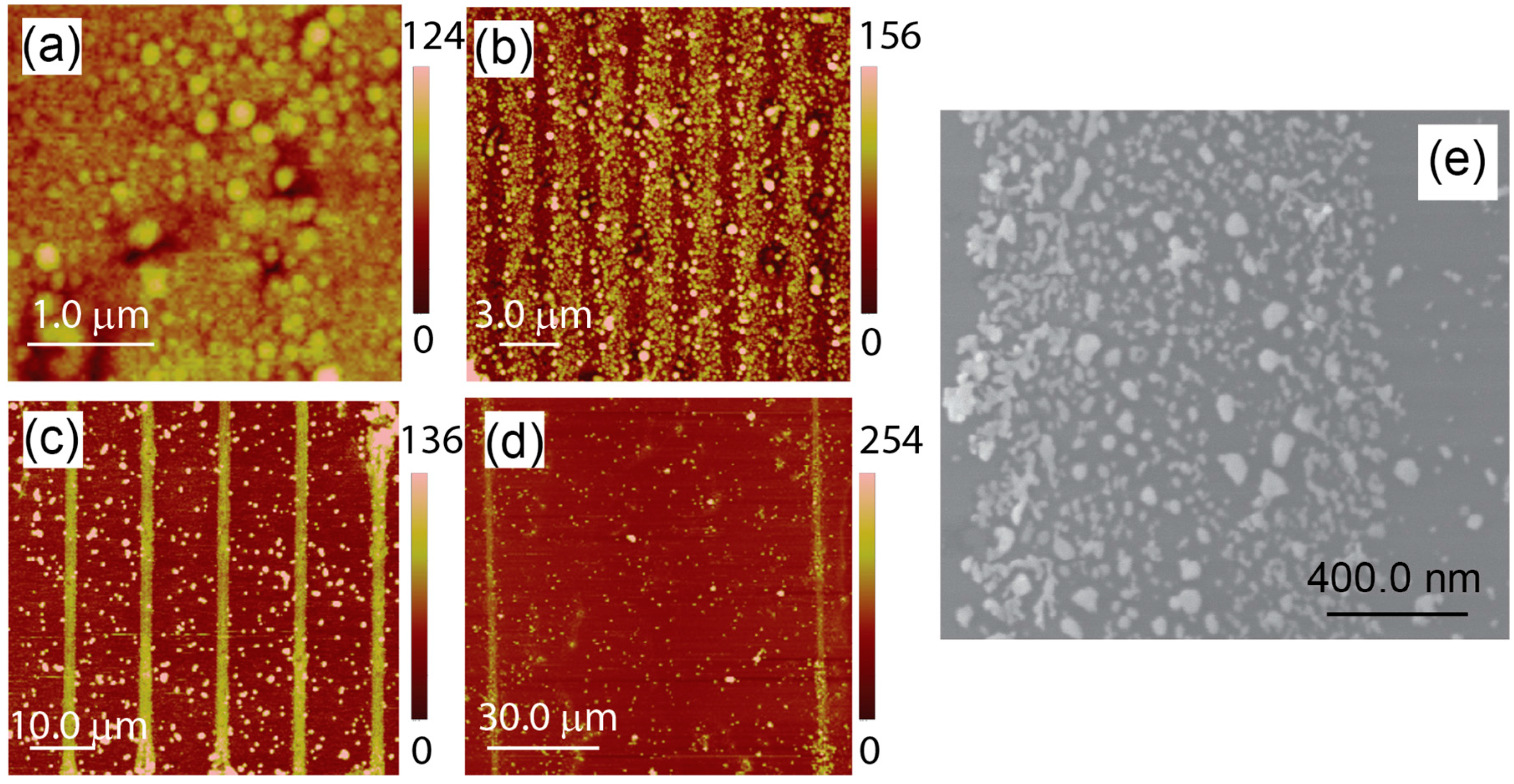
AFM images (
Figure 2a) confirm the obtained arrangement of GNPs in vertical stripes, showing that the diameter of the nanoparticles, depending on the local concentration of the gold precursor and the energy dose delivered by the laser, varied over two orders of magnitude, with the largest value of the order of 100 nm. However, for all the samples we observed an average height of approximately 40 nm, measured by the AFM observation.
It is worth noting that the GNPs with a diameter of the order of 100 nm are due to a greater local concentration of gold ions; therefore, this effect was less visible in the stripes from 0.5 µm to 2 µm where the highest concentration of gold ions was photo-reduced in the first path of the writing beam. This led to a consequent creation of smaller GNPs, characterized by a lower polydispersivity.
In order to estimate the average size of the GNPs, a testing sample with only one stripe was prepared, obtained with the same energy dose used for the fabrications of the other samples. Scanning electron microscopy analysis was performed on this sample, characterized by a length of 1 mm and a width of 1.5 µm (
Figure 2e). By using the same
write-parameter (energy dose) we are sure to obtain a stripe characterized by the same number of GNPs. By means of Image-J software [
28] we counted and determined the size distribution of the GNPs in this stripe, obtaining a density value of 90 µm
−2. This value was used to calculate the density of the GNPs in each sample.
The statistical analysis confirms that all the samples exhibited an average NP diameter of approximately 40 nm. Moreover, they presented a surface density of 1.8 × 10⁸, 4.5 × 10⁷, 9 × 10⁶ and 9 × 105 mm−2, respectively, for the samples with grating periods of 0.5, 2, 10 and 100 µm.
During the direct laser writing, the two-photon absorption induced a local heating of the photo-resist, which led to the thermal photo-reduction of the metallic precursor in the area surrounding the stripes and the creation of random GNPs between them. These random nanoparticles were observed in all four samples and presented a density of 0.5 × 105 mm−2, which did not affect the total density of the samples nor give a consistent macroscopic contribution.
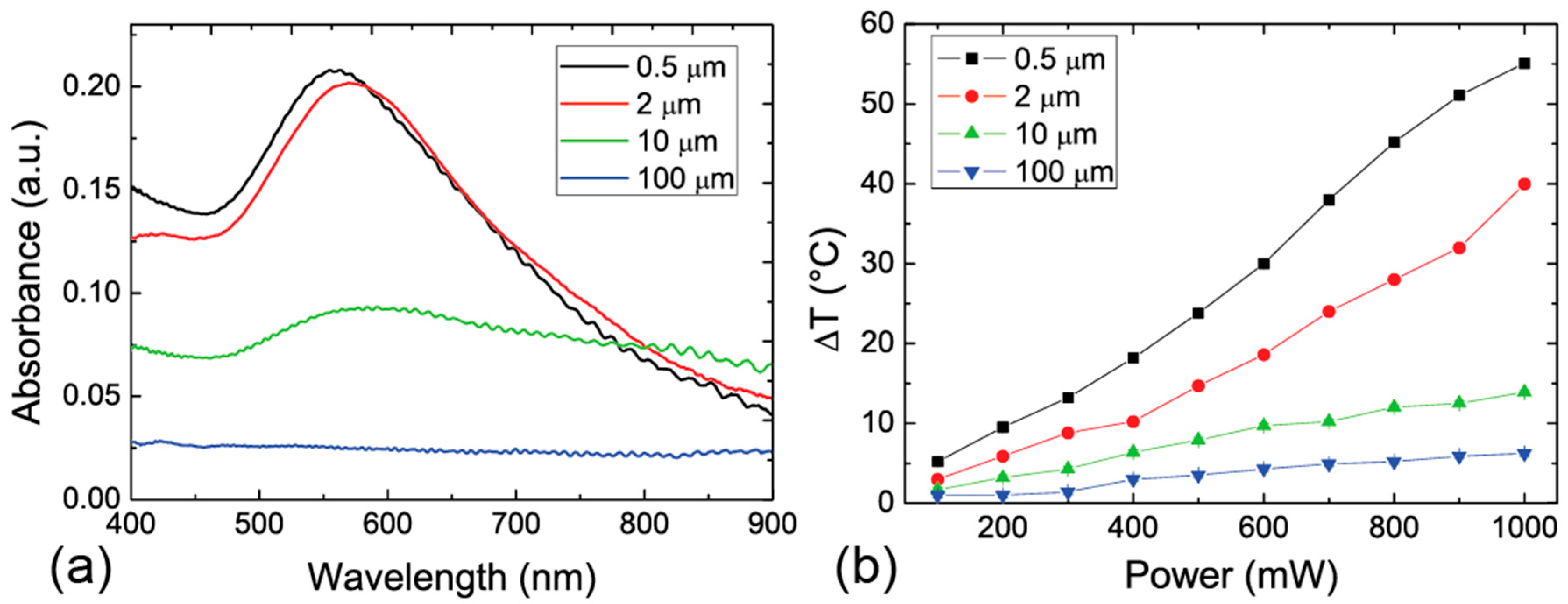
The absorbance spectra (
Figure 3a), obtained by probing the sample with unpolarized white light (wavelength in the range of 400–900 nm) at normal incidence, exhibit the typical gold LSPR absorption band centered at 560 nm for the GNP grating with a period of 0.5 µm, at 575 nm for the GNP grating with a period of 2 µm, at 587 nm for the GNP grating with a period of 10 µm, while, in the case of the grating with a period of 100 µm, we could not see a plasmonic band. The broadening of the LSPR peak is due to the size dispersion of GNPs, revealing that the high density of smaller nanoparticles in the samples with a 0.5 µm and 2 µm period led to a blue-shift in the spectrum resonance [
29].
Thermal analysis was carried out by illuminating the samples orthogonally with a continuous green laser at λ = 532 nm, with a beam diameter of (2.25 ± 0.22) mm. Measurements were made at power intervals of 50 mW in the range of 50–550 mW, corresponding to intensity variations from 1.26 to 13.84 W/cm
2. The photo-induced temperature variation was monitored by using a thermo-camera (E40 by FLIR) characterized by a sensitivity of 0.07 °C and a spatial resolution of 2.72 mrad. The camera control parameters were appropriately set to consider both environmental and materials properties (room temperature, level of humidity in the room, emissivity of the material). By detecting the highest temperature value
T, corresponding to the central pixel of each hot-spot shown in the thermographic images, it was possible to plot the characteristic temperature variation
ΔT ≡ T – T0 as a function of the impinging power density (
Figure 3b, here
T0 is the room temperature). A linear increase was observed in all the samples.
The measured temperature variation results were 55.1 ± 0.3, 40.0 ± 0.3, 13.9 ± 0.3, and 6.2 ± 0.3 °C, respectively, for the samples with 0.5, 2, 10 and 100 µm grating periods.
The same values of ΔT were detected by monitoring different areas of the same sample. Morphological analysis carried out after the thermal test showed that the distribution of the NPs was not affected by the laser exposure. As we can see from experimental measurements, the temperature variations ΔT strongly depend on two parameters: (i) the GNPs’ surface density and (ii) the intensity of the pump beam.
By increasing the power density of the pump beam, T increased linearly until it reached saturation, while variations in the GNPs’ stripes pitch resulted in a change in the P-T curve slope.
By following the fabrication protocol described in this work we can easily control the photo-induced temperature variations by acting on the number and the distance between the GNP stripes. It represents a really fast and simple way to obtain integrable, on-chip, photo-thermally active areas.
3. Materials and Methods
Samples preparation. The technique and materials used are described in reference [
27]. Briefly, a herbium laser, with central wavelength at 780 nm, pulse duration of 100 fs and repetition rate of 80 MHz, is used to perform direct laser writing. The laser beam is focused on the sample through a 63× objective, with a Numerical Aperture (N.A.) equals to 1.4.The transversal position is controlled through a galvo scanner.
The sample is prepared by mixing and stirring for 24 h at room temperature 9.5 mg tetrachloroauric acid tetrahydrate (HAuCl4·3H2O) dissolved in 2 mL of H2O with a solution of 1.3 mg PVA (Mw: 13.000–23.000 g/mol) in 2 mL H2O (98% hydrolyzed). The mixture, photosensitive at 400 nm, was drop-casted on the glass substrates and left to dry for 1 h, before the writing process.
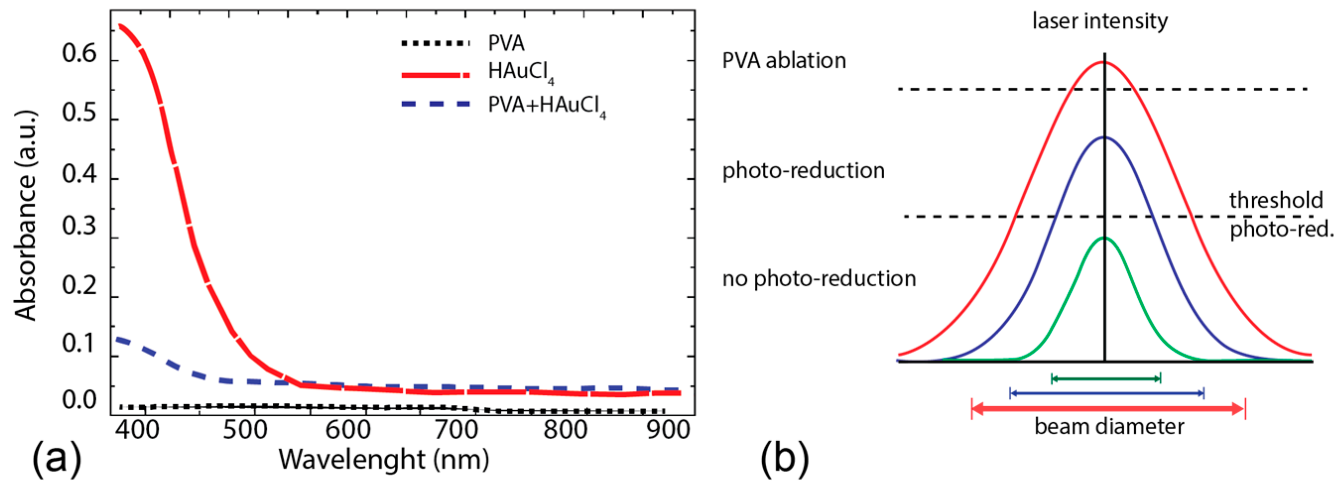
As shown by the graphic (
Figure 4a), a solution of PVA in water is not sensitive to 780 nm radiation. HAuCl
4 can be photo-reduced if invested with UV light, but through DLW process it is possible to obtain a resolution well below the diffraction limits, due to the non-linear optical process of two photon absorption mechanism, whose cross section is proportional to the imaginary part of the susceptibility at the third order and is a process with a threshold [
30]. In this way the GNPs are photo-reduced only in the focus figure of the laser beam and not in all the irradiated area (see
Figure 4b).
After the 2P-DLW of the GNPs, the samples are developed in distilled water for 30 min, the PVA, at this stage, is totally removed with all the GNPs that are not on the surface, then the samples are left to dry before any characterization.
Thermo-camera parameters. Reflected temperature was set to T0 = 20 °C, emissivity of glass to ϵ = 0.83 and the working distance between camera and object was adjusted to the allowed minimum value, i.e., less than 10 cm. The instrument provides images of 19200 pixels (160 × 120 px), where each pixel represents a temperature value.
Atomic Force Microscopy. No contact mode atomic force microscopy (AFM) (Catalyst, Bruker-Nano, Santa Barbara, CA, USA), was employed for the analysis of sample substrates by using silicon tips (radius 8 nm) on a Antimony (n) doped Si lever.
Scanning Electron Microscopy. Morphological analysis was carried out by using a Quanta 400 (Hillsboro, OR, USA) by Fei Scanning Electron Microscope (SEM). The measurements were performed at 0.9 mbar and 15 kV.
Spectrometer. The spectral analysis on the samples was carried out by means of AvaSpec-ULSD2048 spectrometer by AVANTES (Apeldoorn, The Netherlands).
4. Conclusions
In this work a characterization of the photo-induced heat delivered by GNPs arranged in stripes onto a solid flat substrate was carried out. The samples were obtained by means of a direct laser writing technique based on a two-photon photo-reduction process, used on a PVA matrix doped with HAuCl4.
We created four 1D gratings of 1 mm2 rich in gold nanoparticles, with different periods of 0.5, 2, 10 and 100 µm. The morphologic characterization was carried out through AFM and SEM imaging, which allowed for measuring the density of GNPs in the four samples. Irradiating the gratings with a continuous green laser at different power values, we were able to induce a consistent temperature variation from 6.2 ± 0.3 °C to 55.1 ± 0.3 °C.
These results demonstrated that by controlling the stripes’ pitch in the obtained 1D gratings of GNPs, we could control the number of GNPs excited at the same time and the resulting macroscopic temperature variations, paving the way for a wide range of applications in many fields, such as sensing platforms, solar energy harvesting and thermo-catalysis.


