Review

A Review on the Pathways of the Improved Structural Characteristics and Photocatalytic Performance of Titanium Dioxide (TiO2) Thin Films Fabricated by the Magnetron-Sputtering Technique

1
Department of Environmental Science and Engineering, National Pingtung University of Science and Technology,1 Shuehfu Rd., Neipu, Pingtung 91201, Taiwan
2
Department of Physics, Indian Institute of Technology (Indian School of Mines) Dhanbad, Jharkhand 826004, India
3
Department of Environmental Engineering and Science, Feng Chia University, 100Wenhwa Rd., Seatwen, Taichung 40724, Taiwan
4
Emerging Compounds Research Center (ECOREC), National Pingtung University of Science and Technology, 1 Shuehfu Rd., Neipu, Pingtung 91201, Taiwan
*
Author to whom correspondence should be addressed.
Catalysts 2020, 10(6), 598; https://doi.org/10.3390/catal10060598
Submission received: 26 April 2020 / Revised: 22 May 2020 / Accepted: 25 May 2020 / Published: 27 May 2020

Abstract

:
Titanium dioxide (TiO2) thin films are used for a broad range of applications such as wastewater treatment, photocatalytic degradation activity, water splitting, antibacterial and also in biomedical applications. There is a wide range of synthesis techniques for the deposition of TiO2 thin films, such as chemical vapor deposition (CVD) and physical vapor deposition (PVD), both of which are well known deposition methods. Layer by layer deposition with good homogeneity, even thickness and good adhesive nature is possible by using the PVD technique, with the products being used for photocatalytic applications. This review studies the effects of magnetron sputtering conditions on TiO2 films. This innovative technique can enhance the photocatalytic activity by increasing the thickness of the film higher than any other methods. The main purpose of this article is to review the effects of DC and RF magnetron sputtering conditions on the preparation of TiO2 thin films for photocatalysis. The characteristics of TiO2 films (i.e., structure, composition, and crystallinity) are affected significantly by the substrate type, the sputtering power, the distance between substrate and target, working pressure, argon/oxygen ratio, deposition time, substrate temperature, dopant types, and finally the annealing treatment. The photocatalytic activity and optical properties, including the degree of crystallinity, band gap (Eg), refractive index (n), transmittance (T), and extinction coefficient (k), of TiO2 films are dependent on the above- mentioned film characteristics. Optimal TiO2 films should have a small particle size, a strong degree of crystallinity, a low band gap, a low contact angle, a high refractive index, transmittance, and extinction coefficient. Finally, metallic and nonmetallic dopants can be added to enhance the photocatalytic activity of TiO2 films by narrowing the band gap.

1. Introduction

Titanium dioxide (TiO2) is a low-cost non-toxic oxide semiconductor that is extensively employed in various industries due to its optical, electronic, and photocatalytic properties. It is mostly used in thin film form, which enhances the quantum efficiency. Because TiO2 has high transparency and a high refractive index, it can be employed for optical coatings such as those for dielectric interference filters [1], multilayer mirrors, and anti-reflection coatings [2]. Its high dielectric constant and lower resistivity (~10−7Ω·cm−1) give TiO2 the potential for use in the fabrication of capacitors for microelectronic devices [3,4]. In addition, the high chemical stability and modest band gap of TiO2 make it suitable for fabricating dye-sensitized solar cells [5] and photocatalysts. Photocatalysis using TiO2 films has been used to clean up environmental problems [6,7]. TiO2 films have gradually replaced conventional TiO2 powder, which requires stirring during the reaction process and is difficult to separate after the end of reaction [8].
According to electrochemical properties, TiO2 is typically characterized as an n-type semiconductor [9]. TiO2 can exist as an amorphous layer or one of three crystalline phases: anatase (tetragonal, a = 0.3785 nm, c = 0.9514 nm), rutile (tetragonal, a = 0.4594 nm, c = 0.2958 nm), and brookite (orthorhombic, a = 0.9184 nm, b = 0.5447 nm, c = 0.5145 nm) (Figure 1). In all crystalline forms of TiO2, titanium atoms surrounded by six oxygen atoms form TiO6 [10]. In the anatase phase, corner (vertice)-sharing octahedra form (001) planes (Figure 1a) and result in a tetragonal structure. In the rutile phase, the octahedral share edges at (001) planes, therefore, forming a tetragonal structure (Figure 1b). In the brookite phase, both edges and corners are shared, which create an orthorhombic structure (Figure 1c) [11].
The thermal stability of crystallineTiO2 is affected by the film structure and particle size [10]. Rutile is a thermodynamically stable phase, whereas anatase and brookite are metastable. It has been reported that for pure TiO2 films, the metastable anatase phase can easily transform into the more stable rutile phase at high temperature [12,13]. Each crystalline form has practical applications. Rutile is desirable for optical applications, whereas anatase has suitable photocatalytic properties [14,15]. The bandgaps of anatase, rutile, and brookite are 3.2, 3.0, and ∼3.2 eV, respectively [16]. In photocatalysis, TiO2 is excited by photons with energy equal to or higher than their band gap energy level and electrons on the TiO2 surface are excited to the conduction band (eCB, CB), generating positive holes in the valence band (hVB+, VB) (Equation (1)). Moreover, the CB and VB can further react with water and molecular oxygen, respectively, resulting in the formation of the hydroxyl radical (·OH) (Equation (2)) and the superoxide radical anion (O2·−) (Equation (4)). O2·− subsequently reacts with H+ to generate the hydroperoxyl radical (·OOH) (Equation (6)), and then it may further react with itself to produce H2O2 (Equation (8)). The radicals produced by photocatalysis are powerful oxidants that can efficiently oxidize organic species, with mineralization producing mineral salts, CO2, and H2O (Equations (3), (5) and (7)). For TiO2, the photocatalysis reactions (1) to (8) are listed below [16]:
TiO 2 h v e CB + h VB +
H 2 O + h VB + · OH + H +
· OH + pollutant   H 2 O + CO 2
O 2 + e CB O 2 ·
O 2 · + pollutant H 2 O + CO 2  
O 2 · + H + · OOH
· OOH + pollutant H 2 O 2 + CO 2
· OOH + · OOH H 2 O 2 + O 2
TiO2 films have been modified to enhance their photoelectric properties and make them excitable by visible light (narrowing the band gap) [17]. Many studies have demonstrated that the addition of dopants (metal and non-metal) onto TiO2 films can enhance the effect of photocatalytic activity [16].
Metal dopants can act as electron traps at the semiconductor interface that prevent recombination (see Figure 2) [18,19], and non-metal dopants substitute the lattice O atom in the structure of TiO2 to increase the absorption of light in the visible spectrum (see Figure 3) [20,21].
Moreover, non-metal dopants can also increase the thermal stability of anatase [22]. There are many important parameters which control and enhance the photocatalytic performance of the TiO2 thin films. The parameters are listed as follows: different pathways during reaction process, i.e., nucleation growth, formation of different phases like anatase or rutile, surface area, at the interface of the reactants. TiO2 thin films can be deposited by some advances techniques like physical vapor deposition (PVD), chemical vapor deposition (CVD), and wet chemical methods including dip coating, spin coating, spray pyrolysis, etc. Moreover, thermal evaporation, reactive sputtering, ion or electron beam evaporation methods are widely used. These mentioned applications are low cost, and easy to access which is preferable for outdoor applications. The disadvantages of these techniques are that they must be followed by secondary process which include drying and annealing of the thin films to increase the stability and crystallinity of the films, which are some of the essential criteria for the desired enhanced photocatalytic activities. Generally, vapor phase methods present various advantages such as well controlled homogeneity and thickness over a large area and good adhesive nature [23]. The CVD method requires higher temperatures (400–900 °C) compared to PVD processes [24]. This disadvantage of requirement of excessive heat can be incompatible with some substrate materials. Some titanium precursors and their byproducts are highly corrosive in nature, which leads to various material handling and storage problems [25]. However, the PVD processes have garnered great interest since they are not limited to deposition only at thermodynamically equilibrium and they run at much lower costs in comparison to CVD processes [26]. There are many PVD methods that are being applied for the deposition of thin films such as oxidation, deposition, DC magnetron sputtering, RF magnetron sputtering, thermal evaporation, pulsed laser deposition (PLD), etc.
Highly homogenous and high-density films are obtained in these processes due to bombardment of energetic particles, thus these energetic hot particles take part in the photocatalysis process followed by surface plasmon resonance mechanism [27]. This method yields highly porous and dense films at relative low temperatures. TiO2 thin films prepared in this technique can exhibit diverse photocatalytic activities, including high surface area, morphology, defect density, and crystallization pathways. In comparison with TiO2 bulk nanoparticles, TiO2 thin films exhibit a limited surface area, which hinders the efficiency of the photocatalysis for the decomposition of the organic compounds [28]. Thus, various strategies are reported to enhance the surface area of thin films for higher photocatalytic dye degradation studies, where novel sputtering methods are established to produce highly porous thin films for better adsorption of the dye molecules on the surface of the photocatalyst TiO2 thin films. Suzuki et al. [28] have reported a sculptured TiO2 thin film providing a higher photocatalytic efficiency. To achieve a high surface area, nowadays another effective process is established, namely to control nano-crack network formation within sputter deposited TiO2 thin films [29,30].
This review is focused on the effect of magnetron sputtering conditions on TiO2 films. Magnetron sputtering allows the structure and composition of TiO2 films to be easily controlled, yields uniform films, and is suitable for large-scale industrial production. Thus, the optimal operating conditions for magnetron sputtering are of interest. The considered operating conditions, which influence the quality of photocatalytic thin films (PTFs) during magnetron sputtering, are the substrate type, sputtering power, distance between substrate and target, working pressure, argon/oxygen ratio, deposition time, substrate temperature, dopant type, and annealing treatment.

2. Working Principle of Magnetron Sputtering Technique

DC magnetron sputtering techniques are used for depositing thin films over large areas. The continuous current glow discharge that originates the energetic particles that support sputtering process can be obtained by applying a potential difference between two electrodes in the presence of a gas (usually argon) kept at low pressure inside a vacuum chamber. The potential difference can be delivered by a continuous current power supply that can provide tens of thousands of volts, depending on the equipment configuration. An electric field is formed between the electrodes separated by a distance d and having a potential difference V due to the presence of electrons formed by processes such as ionization, thermionic emission and collisions between particles. Here ionization is caused by cosmic rays, but it cannot be maintained. A schematic diagram is shown in Figure 4a.
The gas pressure inside the chamber should not be very low in order to allow a collision between electrons and some atoms before the electrons hit the anode. If the gas pressure is very high, the electrons will neither reach enough velocity nor achieve enough energy in order to form new ions or excited species in the collisions. Under the electrical field, positive ions are accelerated towards the cathode while electrons are accelerated towards the anode. Once electrons travel a long enough distance before the collision, they will acquire enough kinetic energy to promote a new ionization. The main difference between the RF and DC magnetron sputtering is that they work in AC source and DC source mode, respectively. The main advantage of using RF sputtering techniques is that they work well with insulating targets. Moreover, the electric field inside the plasma chamber changes with RF frequency, which avoids any charge up effects. A schematic diagram of RF magnetron sputtering is shown in Figure 4b.

3. Effect of Deposition Conditions on Photocatalytic Thin Films

3.1. Substrate Type

Many materials have been used as substrates in magnetron sputtering, including organic materials (cotton fabrics [31] and polycarbonate [18,32]), inorganic materials (glass [16,33,34] and quartz [35,36]), metals (wafers of alumina (Al2O3) [37] zinc oxide (ZnO) [38], and stainless steel [39]), and minerals (sapphire [5]). Since the transmittance of PTFs affects the photocatalytic efficiency, materials such as glass and quartz are widely used as substrates due to their high transmittance.
Applying TiO2 coatings on a glass surface is the most commonly used method of fabricating PTFs. Sun et al. [40] reported that TiO2 coated on glass has good antibacterial, disinfectant, antifogging, and self-cleaning properties. PTFs have been deposited using chemical vapor deposition, spin coating [40], the impregnation method [41], electrodeposition [42], the sol-gel process [43], evaporation [44], and other sputtering methods [45,46]. Using magnetron sputtering for fabricating PTFs has several advantages, including a high deposition rate, low substrate temperature, good surface flatness, and high density of the deposited layer. However, many researchers have demonstrated that the sodium ions (Na+) from the glass can diffuse into the TiO2 film at a high substrate temperature [47,48] and this Na+ ion diffusion from the glass can reduce the photocatalytic actively of TiO2 films. In order to restrain Na+ ion diffusion, many researchers have applied a silicon (Si) pre-coating on the glass [49]. Meng et al. [50] and Nair et al. [36] used a quartz substrate to prevent light refraction and Na+ ion diffusion. Many researchers have found that a metal oxide coating on the surface of glass (e.g., indium tin oxide (ITO) [51,52,53] and fluorine-doped tin oxide (FTO) [32,54]) can increase the electrical conductivity, however, the photocatalytic activity of TiO2 films mainly depends on the crystalline structure of the surface, not the substrate type [32].

3.2. Sputtering Power

Sputtering power is an important parameter for fabricating TiO2 films via RF [33,55,56,57] and DC [58] sputtering. The crystal phase of TiO2, which affects photocatalytic activity, strongly depends on the sputtering power used [34,58,59,60].
Chen et al. [32] investigated the effect of RF power on the photodecomposition of the dye methylene blue (MB). The results showed that an increase in RF power during TiO2 film fabrication decreases subsequent MB photodecomposition. This result is consistent with that reported by Huang et al. [59] that RF power has a significant influence on MB photodecomposition. This can be attributed to changes in the crystalline phase, surface morphology, and optical properties caused by RF power.
TiO2 exists in an amorphous phase or one of three crystal polymorphs, namely anatase (tetragonal), rutile (tetragonal), and brookite (orthorhombic). These crystalline phases can be prepared using magnetron sputtering [12]. Huang et al. [59] fabricated TiO2 films at increasing RF powers (50–250 W) and observed the conversion of the crystalline phase using X-ray diffraction (XRD). Their results showed that the rutile phase is the favored structure during deposition. With an increase in RF power during deposition, the amorphous, rutile, and a combination of rutile and anatase phases are obtained in sequence. Nevertheless, the anatase phase content levels are similar (in the range of 34% to 37%) at all RF power levels. Sputtering power also affects the elemental composition of the deposited films. The bonding condition of titanium on the surface of TiO2 films can be investigated by X-ray photoelectron spectroscopy (XPS). Lin [58] and Lin and Wu [61] found that Ti4+ forms compared favorably to other types of titanium ion and that the deposited films become non-stoichiometric with increasing sputtering power density, as determined using XPS. The components with the highest and lowest energies on TiO2 films were Ti4+ and Ti0, respectively. The intermediate components (Ti3+, Ti2+, and Ti+) have an energy shift, with resulting energies that fall between those of Ti4+ and Ti0.Substantial contributions from lower oxidation states (Ti3+ or Ti2+ and Ti+) are their large oxygen deficiency. The photocatalytic activity of TiO2 mainly depends on the crystallinity and density of surface defect sites [61]. Liu et al. [62] reported that the dominant defects on TiO2 surfaces are Ti3+ defects and oxygen vacancies. Ti3+ is considered to be an important reactive agent for many adsorbates. Hence, some studies have suggested that Ti3+ sites might play an essential role in the photocatalytic process over a TiO2 photocatalyst [61,63]. Su et al. [60] studied the orientation transformation of crystalline TiO2 film for various RF powers. The sputtering power was set in the range of 100 to 300 W. The results showed that the schematic phase diagram of the crystalline phases can be divided into four regions, as shown in Figure 5.
An anatase-preferred orientation transformation between (101) and (112) is observed. At low total pressure conditions (<11.5 mTorr), anatase (101) exists at low sputtering power (200 W), whereas mixed anatase and rutile phases formed at high RF power (200 to 300 W). Anatase (112) is obtained only at high levels of RF power and high total pressure. These findings are confirmed by using a high RF power, resulting in a mixture of highly crystalline anatase and rutile phases [55]. Rutile is a thermodynamically stable phase, whereas anatase and brookite are metastable. Therefore, the rutile phases of TiO2 films are formed with high sputtering power. In addition, these results imply that the crystalline phase of TiO2 in turn becomes amorphous, anatase, and rutile as the sputtering power is increased. The efficiency of photodecomposition of anatase phase in TiO2 films is found to be better than those of amorphous, rutile, brookite, and anatase/rutile phases [64]. Bombardment on the substrate at higher power may cause film damage and decrease compactness, which can be an obstacle to rutile growth [55]. This trend has also been reported by Chow et al. [65], who found a similar effect of negative-bias-induced bombardment.
Film density is also directly affected by sputtering power. It has been well established that the refractive index is closely correlated with film density [66]. Many researchers found that the refractive index increases with increasing sputtering power [34,35,67]. Theoretically, for a well-balanced magnetron, the power per sputtered adatom increases with increasing total sputtering power, delivering more energy to the growing film and thus improving densification. Therefore, a higher refractive index (n) means a denser film [34] and a finer film nano/micro-structure [37,68,69]. In addition, the refractive index of a transparent thin film is directly proportional to its electronic polarization, which is in turn inversely proportional to the inter-atomic separation [1]. The refractive index of TiO2 films also depends on porosity (volume of pores per volume of film) of the film layer and can be calculated using the Swanepoel method [1,35,68,70] (Equations (9) and (10)). The porosity of the deposited film was calculated from the refractive index obtained from previous studies [70,71,72] (Equations (10) and (11)). From the refractive index, the porosity of each sputtered film can be derived using Equation (12) [72].
N = 1 2 ( 1 + n s 2 ) + 2 n s ( T max T min ) T max · T min
n = N + N 2 n s 2
ρ film ρ = n 2 + 1   n film 2 1 n 2 1   n film 2 + 2
P o r o s i t y ( % ) = ( 1 ( n p 2 1 ) ( n 2 1 ) ) × 100
where Tmax and Tminare the corresponding transmittance maximum and minimum, respectively, at a certain wavelength λ in the optical transmittance spectrum (for determination of Tmax and Tmin, refer to [69]). ns is the refractive index of fused quartz. ρfilm is the film density, ρ is the bulk anatase TiO2 density (3.9 g/cm3) or rutile TiO2 density (4.23 g/cm3), nP is the refractivity of porous thin films, and n is the refractivity of bulk TiO2. As is well known, the refractivity of bulk anatase TiO2 is na= 2.52 and that of rutile TiO2 is nr = 2.92 at 500 nm [72].
Nair et al. [36] attributed the increase in the refractive index to the densification of layers treated at a high RF power. Since the densification of layers is correlated with the thickness of the films, an increase in the sputter power increases the deposition rate at the target [57,73]. Yang et al. [35] found that a high sputtering power can increase the surface roughness of the film, which results in decreased transmittance [57,74]. The surface roughness affects the contact angle of films; the contact angle increases with roughness [75]. Many researchers have demonstrated that the rutile phase is more hydrophilic than the anatase phase [74,76,77]. Therefore, the sputtering power is an importer factor when the magnetron sputtering process is used to fabricate TiO2 films. It also directly influences the crystalline phase (including elemental composition), optical properties, and physical characteristics of deposited films.

3.3. Distance between Substrate and Target

Relatively little research has been conducted on the effect of the distance between substrate and target (S-T) on the crystalline phase of TiO2 films during the magnetron sputtering. Ogawa et al. [15] have investigated the crystalline phase of TiO2 films obtained with various S-T distances during RF magnetron sputtering with an MgO substrate. According to XRD results, the crystalline structure of TiO2 changes with S-T distance. When the S-T distance is under 90 mm, the rutile phase of TiO2 film is dominant. At an S-T distance of 100 nm, mixed rutile and anatase phases are observed. At S-T distances of 110 and 120 mm, the anatase phase is dominant, with epitaxial growth with its α-axis perpendicular to the MgO substrate. Shibata et al. [78] reported that the anatase phase grows from the reaction between neutral Ti and neutral O2 or O2, and that the rutile phase results from the reaction between decelerated Ti+ or activated Ti and O2. Hence, more anatase TiO2 film is created at low kinetic energy of sputtering compared to rutile TiO2 film [59]. This result implies that the crystal structure shift is due to the reaction of sputtering particles between the substrate and the Ti target. When the substrate bias voltage is increased, the electrons in the plasma bombarded Ti atoms, creating Ti+ or activated Ti, resulting in increased formation of rutile TiO2 [79]. In the magnetron sputtering process, a magnetic field configured parallel to the target surface can constrain secondary electron motion to the vicinity of the target [80]. Therefore, a decrease of S-T distance (increase in magnetic field range) increases the kinetic energy of sputtering, and thus rutile TiO2 film is formed under this sputtering condition. While the S-T distance increased resulting in the decrease of magnetic field strength, secondary electrons can easily recombine in the plasma, resulting in a decrease in the kinetic energy of sputtering and the formation of anatase TiO2 film.
The S-T distance also affects the deposition rate and particle size. Sundaram and Khan [81] found that a 2–7 cm distance between S-T during the magnetron sputtering process decreases deposition rate due to a large number of negative and neutral ions in a small space, which led to the occurrence of resputtering on the surface of the growing film. Regarding particle size, Barnes et al. [82] indicated that the clusters nucleate close to the target and migrate to the substrate via convection. A small S-T distance limits convection, leading to an almost uniform cluster size and small grain size. An increase in S-T distance increases convection space, and thus leads to an increased size distribution of clusters and grain size on TiO2 films. This phenomenon has been observed in metal evaporation systems [83]. The grain size influences the photocatalytic activity of TiO2 films [18,84]. Using the Scherrer Equation, the crystalline grain size can be calculated from an XRD pattern as:
D = 0.9 × λ B cos θ
where D is the mean grain size for crystalline planes, B is the full width at half maximum (FWHM) intensity in radians, and λ is the wavelength of the Cu Kα radiation source. Many researchers have reported that smaller particles enhance photocatalytic activity [18,85,86] due to the decrease of distance between the crystal interface and the surface of the substrate [87]. Smaller particles induce the quantum size effect, which influences the optical absorption edge of the films, resulting in an increase of the band gap and the absorption onset blue-shift. Therefore, photocatalytic activity increases with increasing oxidation rate. For large particles, the e/h+ volume recombination is the dominant process. An appropriate S-T distance is thus important when fabricating TiO2 films using magnetron sputtering.

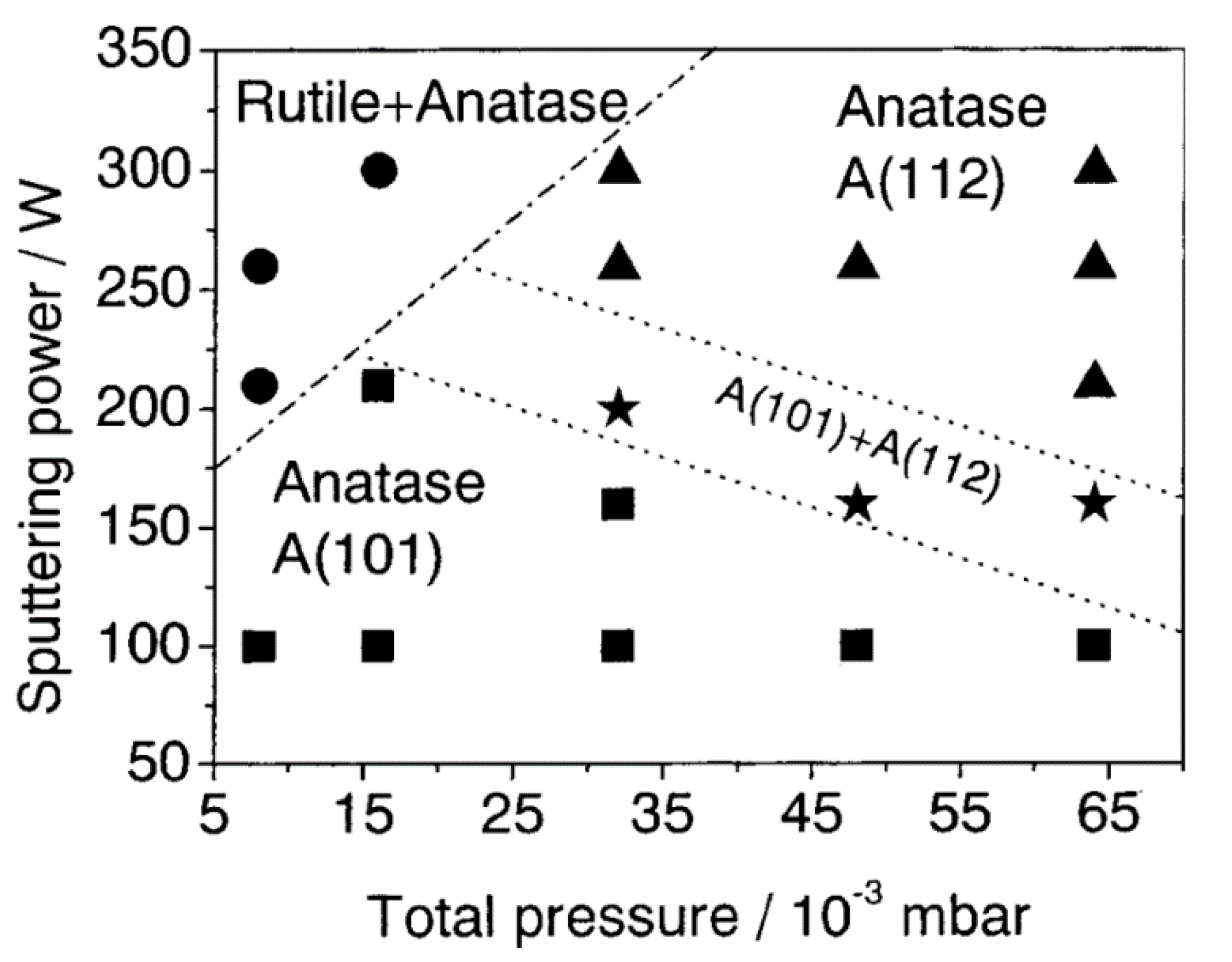
3.4. Working Pressure

The deposition rate, surface morphology, and crystalline phase of TiO2 films are affected by the working pressure during the sputtering process [14,87,88]. The working pressure directly affects the photocatalytic activity of TiO2 films since it affects the gas collisions, which affect the characteristics of deposited films. Many researchers have also reported that the photocatalytic activity of TiO2 films is significantly correlated with the working pressure [8,89]. For example, TiO2 films with high photocatalytic activity can be prepared using a relatively low-working pressure [90]. Thus, specific parameters of deposited films are influenced by the working pressure, namely the deposition rate (thickness), surface morphology, and crystal phase of TiO2 films.
The effect of working pressure in the sputtering process on the deposition rate has been investigated by many researchers [14,87,91]. Zeman and Takabayashi [14] found that the increasing working pressure (0.18—1.50 Pa) significantly decreases the deposition rate during magnetron sputtering (Figure 5). Zhu et al. [91] obtained different experimental results when using ZnO and Al to fabricate films. They measured the deposition rate for fabricating ZnO-Al films at various working pressures. The experimental results showed that the deposition rate is low at low working pressure (0.5 Pa) and then it increases with the working pressure up to 1.0 Pa. Above 1.0 Pa, the deposition rate is decreased with increasing working pressure. They also found that the decrease in deposition rate with higher working pressure (above 1.0 Pa) can be fitted using the Keller-Simmons model [92], which suggested a decay of the deposition rate at high pressures is caused by shielding effects of gas particles between the target and substrate. Nevertheless, the low deposition rate at low working pressure can be explained by the resputtering of ZnO by highly energetic particles, which are more prevalent at lower pressure. Chaoumead et al. [87] used RF magnetron sputtering to deposit ITO thin film on glass substrates. The trend of the deposition rate of the ITO film was similar to that reported by Zhu et al. [91]. Decreases in deposition rate of ITO film is observed when the working pressure is increased from 5 to 15 mTorr (low working pressure). When the working pressure is further increased to 20 mTorr yielding decreases in the deposition rate. Finally, it is clear that the surface morphology is affected by the working pressure.
Scanning electron microscopy (SEM) [14,92] and atomic force microscopy (AFM) [89,93] can be applied to observe the surface morphology of PTFs. In PTFs, the particle size influences surface morphology. Many researchers have demonstrated that particle size depends on sputtering pressure [88,89,94]. It has been suggested that the pressure influences the energy transfer from the applied electric field to the species present in the discharge, and thus increasing the sputtering pressure results in an increase in the number of gas-phase collisions and a reduced fraction of particles with sufficient energy reaching the TiO2 film [95]. In other words, higher sputtering pressure leads to lower ion kinetic energy, which decreases the particle size [96]. Jin et al. [88] indicated that the surface morphology is strongly influenced by working pressure. Spherical TiO2 particles are observed on the surface of TiO2 films via field-emission SEM. When the working pressure is increased from 5 to 10 mTorr, the grain size of TiO2 particles decreased from 35 to 25 nm. The working pressure thus affects the grain size of TiO2 particles; hence, increasing working pressure increases surface roughness [97] during the sputtering process. Zeman and Takabayashi [14] also found that working pressure affects surface morphology. A significant change in film density is observed when the working pressure is increased from 1.35 to 15.3 mTorr. Three types of surface morphology are observed. (i) A dense surface with only a few distinct symmetrical particles corresponds to rutile film (working pressure: 1.35 mTorr) [14]. (ii) The anatase surface (working pressure: 4.8 to 9.75 mTorr) is characterized by relatively densely packed surface particles resembling an array of different polygons. These particles have a symmetrical or elongated shape with a size of 10 to 50 nm. (iii) When the working pressure exceeded approximately 1.30 Pa, the surface morphology changed again [14]. The surface obtained at a higher working pressure is less dense, which implies that voids occupy more space and the surface roughness increases. Zhang et al. [93] have confirmed these findings by using AFM (Figure 6)
The surface of TiO2 film deposited at 0.4 Pa is much smoother than that of film deposited at 1.4 Pa. El Akkad et al. [98] found similar results, where rough surfaces are obtained at high working pressures. The change in surface morphology is due to the transition of the crystal phase at high working pressure [14].
Many researchers have found that the anatase phase of TiO2 films is dominant at high working pressure, whereas the rutile phase is dominant at low working pressure [14,87]. Wang et al. [89] showed that the band gap increases with increasing working pressure. This is due to the different content levels of anatase and rutile phases. For wavelengths below 400 nm, the transparency of films sharply decreases in the ultraviolet (UV) region; it is almost constant for wavelengths above 400 nm. This decrease is caused by the fundamental absorption of light [99]. This phenomenon is due to the quantum size effect when the particle size is very small [100]. Nair et al. [36] found that the increase in porosity with increasing sputtering pressure results in a decrease of the refractive index. This suggests that sputtered particles undergo more scattering and that fewer atoms reach the substrate, resulting in lower crystallinity at high working pressure.
The absorption coefficient (α) can be expressed as [36,90,100]:
α = d 1 ln ( 1 T )
where T is the transmittance and d is the thickness of the film.
The band gap energy (Eg) can be calculated based on the absorption spectra using [36,94]:
α h v = A ( h v E g ) n / 2
where α, hv, Eg, and A are the absorption coefficient, light frequency, band gap energy, and a constant, respectively. The value of n depends on the type of optical transition of the semiconductor (n = 1 for direct transition and n = 4 indirect transition). TiO2 has been demonstrated to have both directly forbidden and indirectly allowed transitions. The indirectly allowed transition dominates the optical absorption because the directly forbidden transition is weak. The value of the direct optical band gap is obtained by plotting (αhv2) versus hv (Taucplot) in the high-absorbance region. Extrapolating the linear portion of the graph to the X axis yields Eg, which is the sum of terms correlated to carrier concentration [17], structural disorder [1], and thermal contribution [101].
An increase in the working pressure can effectively increase the density of gas particles in the chamber and decrease the cathode potential, which may further influence the probability of collisions and the acceleration of particles, resulting in changes in the crystalline structures formed. Šícha et al. [97] obtained the following results: (i) For the formation of amorphous TiO2 film, the energy E delivered to the deposited film decreases when the working pressure is below 2 Pa, and is thus insufficient to stimulate film crystallization. (ii) For the formation of rutile TiO2 film, crystalline phases are formed at low values of PT (total pressure) and PO2 (oxygen pressure) when the energy E (incident and condensing atoms) is sufficient for the crystallization and is delivered to the deposited film. The energy E increases with decreasing PT in consequence of a decrease of collisions between particles. In addition, the condition of low PO2 can change the chemical process, contributing to the formation of the rutile phase. (iii) For the formation of anatase TiO2 film, crystalline phases are formed when the working pressure is higher than 2 Pa. The increase of sputtering time also ensures that a sufficient amount of energy is delivered to the deposited films and stimulates the crystallization of the anatase phase. In addition, Zeman and Takabayashi [14] found that the boundary between the metallic and reactive modes shifts when the working pressure and the ratio of PO2/PT are increased.
The change in crystalline phase of TiO2 films is not only affected by the working pressure but also the argon/oxygen ratio in magnetron sputtering.

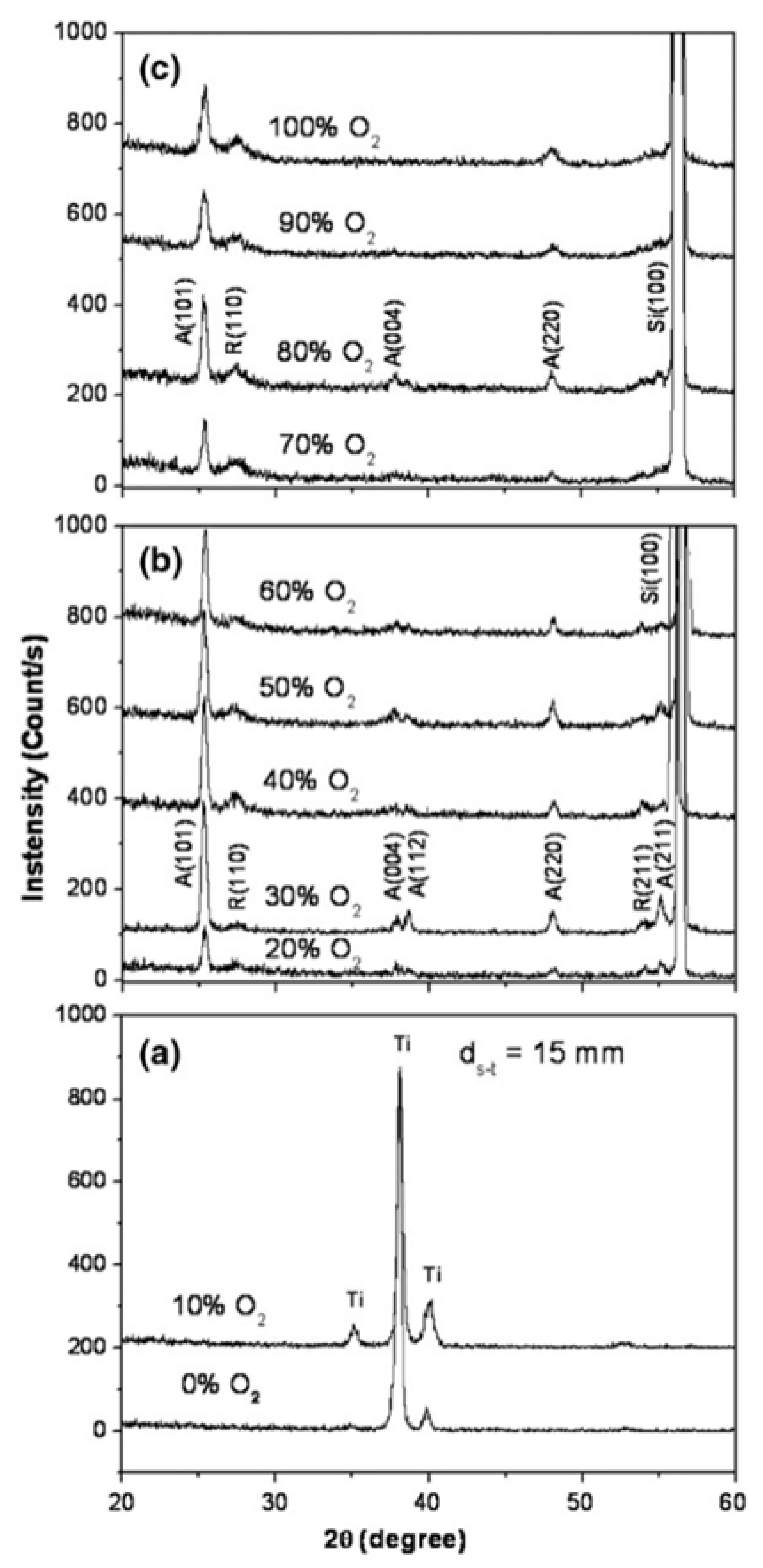
3.5. Argon/Oxygen Ratio

During magnetron sputtering, argon and oxygen serve as the plasma gas and the reactive gas, respectively. Thus, the oxygen partial pressure may influence the discharge parameters, such as plasma potential, discharge voltage, deposition rate, and ion composition of the discharge, and thus the characteristics of TiO2 films in the magnetron sputtering process [14]. Although numerous attempts have been made to study the relationship between the argon/oxygen ratio and photocatalytic activity, no clear consensus has been reached. Zhang et al. [101] found that TiO2 film deposited at a high argon flow rate absorbs lighter irradiation, which results in more electron-hole pairs generated in the TiO2 film and thus enhances photocatalytic activity. Huang et al. [66] reported that the photocatalytic activity of TiO2 films increases with increasing oxygen flow rate. These results differ from those reported by Chiou et al. [33], who found that the argon/oxygen ratio and the photocatalytic activity of TiO2 films are not significantly related. Since the photocatalytic activity of TiO2 depends on the strength of the crystalline phase and the characteristics of the deposited films, the effect of the argon/oxygen ratio on the characteristics of TiO2 films needs further study.
The effects of the argon/oxygen ratio on the photocatalytic activity of TiO2 films have been extensively investigated. Many researchers have found that a lot of properties of TiO2 film are affected by the argon/oxygen ratio in magnetron sputtering, including the deposition rate [62,74,82,102,103], grain size and surface roughness [37,76,87,104], crystallinity and surface chemical composition [33,86], and optical properties [1,37,62,105]. The dissociation energy of argon is about 15.76 eV and that of oxygen is about 48.77 eV. Thus, argon gas is more easily dissociated [33].
The deposition rate decreases slowly with increasing proportion of oxygen (Figure 7) [62,74,102,103]. Pradhan et al. [105] and Liu et al. [62] suggested that this decrease is due to the transition from metallic to reactive sputtering modes. Tomaszewski et al. [102] investigated the transition mechanism on the surface during magnetron sputtering. They found that increasing the oxygen flow rate led to a significant decrease in the sputtering voltage. In the low-energy state, Ti and O-related species sputtered from a TiO2−x target easily reach the substrate, forming stoichiometric TiO2 films. However, the oxygen of the sputter gas can be decomposed and changed to O ions in the plasma, which are accelerated by the electric field around the target, increasing the opportunity for ion-induced secondary electron emission and thus decreasing the deposition rate. This explanation is consistent with those results reported by Zhang et al. [104].
The grain size and root-mean-square (RMS) surface roughness of TiO2 films are affected by the argon/oxygen ratio in magnetron sputtering [37,76,87,104,106]. Argon is the main sputtering gas that imparts kinetic energy to the sputtered atoms. The partial pressure of oxygen can affect particle collisions and the mobility and diffusion of the species approaching the substrate. Studies have found three different phenomena: (i) The grain size increases with increasing oxygen partial pressure. Laha et al. [37] suggested that the increase in the oxygen flow rate decreases the mobility of the sputtered ions, resulting in increased particle size. (ii) The grain size decreases with increasing oxygen partial pressure. Lin et al. [74] and Huang and Hsu [103] reported that the grain size decreases as the percentage of O2 increases. Huang and Hsu [103] found that high oxygen gas content in the sputtering process increases the resputtering effect, which results in insufficient energy for grain growth. (iii) The grain size initially decreases and then increases with further increases in the oxygen partial pressure [86,87]. Regarding the relation of surface roughness and the argon/oxygen ratio, many researchers have demonstrated that the surface roughness decreases when oxygen pressure increases [2,37,76,87,106]. Jeong et al. [2] found that Ti and Si atoms decreased with increasing proportion of oxygen. Laha et al. [37] found that the surface of the films become smooth and flat as a result of increased grain size. However, Xu and Shen [86] found that the RMS surface roughness of TiO2 films decreased with increasing oxygen gas pressure, and that the RMS surface roughness is not related to the grain size. Toku et al. [107] gave a different interpretation of the influence of oxygen pressure on the surface roughness of deposited films. They indicated that increasing the percentage of O2 makes the potential drop across plasma sheath decreases due to the abundant negative oxygen ions formed in the plasma; therefore, the impact of energetic ions on the surface is reduced. This impact may be the reason for the surface is becoming uniform in the absence of impurities. However, Huang and Hsu [103] reported an increase in RMS surface roughness (from 12.3 to 18.1 nm) when the percentage of oxygen is increased from 0% to 20% (argon% + oxygen% = 100%). Water and Chu [106] found a simialr trend, with an increase in the oxygen content there is increasing in the RMS surface roughness of ZnO films. Many researchers agree that both the grain size and surface roughness of TiO2 films are important factors of photocatalytic performance. A small grain size can decrease the recombination of electron-hole pairs [18,86] and a low surface roughness can prevent light scattering [108,109] and thus increase the hydrophilicity of deposited films [76]. However, studies on the effects of the argon/oxygen ratio on the grain size and roughness of TiO2 films have reported mixed results. The optimal argon/oxygen ratio for photocatalytic activity is thus difficult to determine.
The effects of the argon/oxygen ratio on the crystallinity and surface chemical composition of TiO2 films have been investigated in many studies [79,83,105,106,110,111,112]. Oxygen plays an important role in the preparation of TiO2 films via magnetron sputtering. Many researchers believe that the oxygen concentration during magnetron sputtering affects oxygen vacancies, which cause structural defects in the deposited films [37]. Zhang et al. [101] found that the discharge voltage increases with increasing oxygen flow rate up to a certain threshold. With increasing oxygen flow rate, the secondary electron emission in the reaction chamber is also increased. A mixture of metallic Ti and titanium oxides is deposited on the substrate before the threshold is reached. Only after the oxygen flow rate reaches the threshold can a uniform transparent TiO2 thin film form on the substrate
A large secondary electron emission may thus help convert the target into titanium oxides. In addition, the oxygen in the chamber can promote the substitution of Ti in the TiO2 crystal lattice, change the crystallinity of TiO2 films [113], and implant anion species on TiO2 films, leading to changes in the surface chemical composition [79]. Toku et al. [107] deposited TiO2 films at various oxygen concentrations and found that the degree of crystallinity (anatase 101) of TiO2 films is greatest at an oxygen content of 30%, and then decreases with increasing oxygen content (see Figure 8).
The crystal phases of TiO2 films are also affected by the oxygen concentration in magnetron sputtering. When the oxygen concentration is increased, the crystallinity of TiO2 films slightly changes from the anatase phase to a mixture of anatase and rutile phases [14]. However, the authors concluded that working pressure has the most influence on the crystalline phase of deposited films. Tavares et al. [109] also found that the oxygen flow rate influences the crystalline phase of TiO2 films. At flow rates below the 2.4 sccm threshold, the texture is very weak and only a slightly pronounced anatase (101) peak is observed. With increasing oxygen flow rate, other anatase peaks, namely (004), (200), (105), (211), (204), and (106), are enhanced at threshold conditions. When the oxygen flow rate is above the threshold, the crystalline phase of TiO2films gradually changes from anatase to rutile because the latter is more stable. Above 3.6 sccm, the crystal phase becomes amorphous due to the high pressure and inherent reduced adatom mobility. Xiong et al. [110] reported similar results, with TiO2 films showing a phase transition from anatase to rutile when the oxygen flow rate is increased. Kinetic energy (sputtering power or working pressure) is thus not the only factor in determining the crystal phase. Consequently, they inferred that the species sputtered from the target and the surface reactions on the substrates have a large impact on crystal nucleation and growth.
Several researchers have found that the argon/oxygen ratio affects the surface chemical composition. Ti4+ and Ti3+ are dominant species of the elemental compositions. Peaks at 2p3/2 (458.5 eV, TiO2) and 2p1/2 (464.1 eV, TiO2) are observed, representing the existence of Ti4+, when XPS is used to examine TiO2 films fabricated at high oxygen pressure in the magnetron sputtering process. If a high argon pressure is used to fabricate TiO2 films, Ti3+ will be the dominant species and peaks at 2p3/2 (457.5 eV, Ti2O3) and 2p1/2 (463.3 eV, TiO2) will appear in the XPS spectrum [2,62,106,114]. However, the Ti3+ state of TiO2 films may decrease the probability of electron-hole recombination, leading to enhanced photocatalytic activity. Vancoppenolle et al. [115] investigated the reactive species (Ti+, TiO+, TiO2+) are generated on TiO2 films at different argon/oxygen ratios. Ti+ decreases and TiO+ and TiO2+ increases when the oxygen content was increased from 0% to 20%. In addition, O2 is incorporated practically and completely into the growing films at a low flow rate. Barnes et al. [82] provided a schematic of the theory of charged clusters in terms of nanocrystal and thin film growth that is depicted in Figure 9.
This figure shows the nucleation of TiO2 clusters, which is a simulated reaction between Ti and O atoms during the magnetron sputtering process. The clusters are the growth unit for the thin film. Shibata [78] reported that the anatase phase is the result of the reaction between metallic Ti with neutral O2 or O2 and that the rutile phase results from the reaction between ionic Ti+ or activated Ti with O2. Toku et al. [107] used mass spectra to measure the variation of Ti and TiO2 particles on TiO2 films with oxygen content (Figure 10).
They divided the elemental composition of TiO2 films into three categories: metallic, transition, and oxide. The results show that the three regions can be distinguished, since each one describing a different process occurring during discharge. At the condition of pure argon and low oxygen (Region I), the peak of Ti is predominantly due to the bombardment by argon ions. When the oxygen content is increased, an increase in the TiO2+ peak is observed (Region II). With oxygen content higher than 60% (Region III), an increase in oxygen content causes a decrease in the intensity of the anatase phase. As the oxygen is increased, the target becomes gradually oxidized, and consequently fewer Ti atoms and more TiO2 molecules are ejected from the target. TiO2 molecules in magnetron sputtering can originate from either the sputtering of the oxidized target or from the reaction of Ti atoms and O2 molecules being charged. Ti atoms cannot be deposited on the substrate without argon gas in the magnetron sputtering process. Some researchers claim that the overdose of oxygen content in the magnetron sputtering might be responsible for the growth of low-crystallinity films [107].
The optical properties of PTFs is depending on the crystal phase and surface characteristics. The crystal phase of PTFs is affected by the argon/oxygen ratio in the sputtering process. Jeong et al. [2] found that the structural characteristics of both TiO2 and SiO2 are significantly improved with oxygen gas addition in the sputtering ambient compared to those of films grown without oxygen gas. Choi et al. [52] obtained similar results, finding that low mobility could be caused by high oxygen content. Their study showed that the decrease of collisions of Ar/O2 gases during surface diffusion may result in the deficiency of crystallinity of TiO2 films. The band gaps of the rutile and anatase phases are 3.0 and 3.2 eV, respectively. Structural defects in deposited films may also cause a variation in the band gap. The structure of deposited films consists of the UV emission band and the visible emission broad band. UV emission causes exciton recombination, and visible emission is attributed to structural defects, which are related to deep-level emissions [37]. Laha et al. [37] and Tomaszewski et al. [102] found that the argon/oxygen ratio during magnetron sputtering influences the level of oxygen vacancies in deposited films. Therefore, the level of oxygen vacancies is related to the band gap of the deposited films.
Transmittance (T) and the refractive index (n) are also affected by the argon/oxygen ratio in magnetron sputtering. High transparency in the visible range and a proper band absorption edge are very important for self-cleaning applications and photocatalysis. Xiong et al. [110] have investigated the effects of the argon/oxygen ratio in RF sputtering on the optical properties of TiO2 films. They found that light transmittance in the visible range (400–800 nm) is slightly increased when the oxygen content is increased. At wavelengths below 350 nm, a significant drop in transmittance is discovered, which is attributed to the absorption of light caused by the excitation of electrons from the VB to the CB. Laha et al. [37] found that the transmittances of TiO2/Al2O3 films in the spectral range (200–1100 nm) is increased with increasing argon/oxygen ratio. Moreover, the maximum transmittances are red-shifted with increasing argon/oxygen ratio, which can be explained by the particle size effect. Regarding the refractive index (n), Tomaszewski et al. [102] found that it is reduced with increasing oxygen content. They also indicated that the refractive index is correlated with the deposition rate. Kumar et al. [1] found a similar trend for MgTiO3 films fabricated by RF magnetron sputtering at various oxygen content levels. The change in the refractive index is attributed to the packing density and crystallinity of the deposited films. The fabrication of thick TiO2 films requires a long sputtering time and sufficient energy, which results in high packing density. Kumar et al. [1] found that the amorphous nature of deposited films is highly disordered and thus the films have a low refractive index. This is attributed to the low film density and low adatom mobility when the energy applied during the magnetron sputtering is insufficient. The oxygen content affects the crystal phase of TiO2 films and its optical properties. The thickness of TiO2 films also affects these properties.

3.6. Deposition Time

The deposition time is directly proportional to the thickness of deposited films. The influence of thickness on photocatalytic activity is still being debated [8,46,66]. Some researchers hypothesize that photocatalytic activity mainly depends on the crystalline phase and optical properties of PTFs, not thickness [46,66]. Huang et al. [66] found that sputtering power is a more important factor than sputtering time in enhancing photocatalytic activity of fabricated PTF films to decompose MB. Chen et al. [32] revealed that the sputtering time of PTF film fabrication has no effect on the photodecomposition of MB. Jamuna-Thevi et al. [39] used Ag-doped TiO2 coatings on stainless steel to obtain antibacterial properties against Staphylococcus (S.) aureus. The results showed that the level of silver ions affected the reduction of S. aureus, not the deposition time. Nevertheless, Zheng et al. [8] and Eufinger et al. [67] found that film thickness plays an important role in the photocatalytic activity of TiO2 films. The thickness (d) of films can be calculated as [1]:
d = λ 1 λ 2 2 ( λ 1 n 2 λ 2 n 1 )
where n1 and n2 are the refractive indices of two adjacent maximum and minimum at wavelengths λ1 and λ2, respectively.
When the film thickness is below a critical value, the photocatalytic activity of TiO2 films increases with increasing thickness. Once the film thickness exceeds the critical thickness, it has little influence on the photocatalytic activity of TiO2 films. Yang et al. [46] indicated that the deposition time had a dominant effect on MB absorbance. Zhang et al. [104] observed the optical properties of PTFs obtained with deposition times of 2, 3, and 5 h. The results showed that the three kinds of TiO2 film exhibits quantum size effects and that the blue-shift of their band edges is slightly increased with decreasing deposition time. The authors attributed this to increases in the film thickness and grain size, which resulted in complete crystallinity. Rahman et al. [111] shows the deposition of TiO2 homogeneous highly porous thin films by hydrothermal method and enhanced photocatalytic degradation efficiency with increase in film thickness with the increase in titania precursor concentration. They also reported that the thickness can be determined from the transmittance spectra, which shows that the transmittance of the films decreases with film thickness. This phenomenon occurs due to the increase of the atom on the surface because of the increase in deposition time or concentration of the precursor. In another article revealed that on increasing the deposition time of the magnetron sputtering the thickness, crystalline size and resistivity of the films are increased gradually [112]. In addition the structural and electrical properties of the ZnS film has been studied with the variation of film thickness have been investigated. It was observed that with the increasing the deposition time, the crystalline quality could be improved with developing better conducting behavior according to the increase in film thickness [113,116]. The better conducting behavior can increase the generation of the charge carriers on the surface of the material, which is the key reason for the enhanced photocatalytic activity. With the increase in film thickness, the quality of the crystallinity is improved as well as grain size value is increased, with increase in film thickness [117]. All characteristics are enhanced with the increase in deposition time. The roughness of prepared films is acquired from AFM measurements, and their evolutions with deposition time are increased by increasing the thickness, where it increases from 2 nm to a maximum value of 7 nm, when film thickness is from 70 nm to 170 nm, respectively. These results were confirmed by Abdalah et al. [118]. The cross section of the films, investigated from the SEM characterization, can be increased with deposition time and reaction rate. In sputtering technique, the parameters like base pressure, substrate temperature, deposition time and distance between the substrate and target are vital for better films properties. To obtain better optical properties and photo response properties in photocatalysis reactions doping elements, substrate, as well as deposition time can be changed for enhanced results. Abbas et al. [119] has reported in his research that the crystallization of the PbS thin films can be improved by increasing the deposition time and annealing temperature to increase thickness of film. The low value of transmittance in the UV region and increases gradually as the wavelength shifts to the NIR region. It can also be emphasized that the transparency window decreases with the deposition time, due to increasing thickness with time. Thickness of the film increases with increased deposition time or different nature of the substrate. Deposition time can affect the surface roughness by RF sputtering process [115]. The results show the highest roughness of the sample after depositing the films for 10 minutes, but it decreases with a deposition time of 15 minutes [120]. By lowering the amount of surface roughness the rate of surface reactions will increase.
Recent studies [36,117] have found that increased thickness increases the refractive index. This infers that higher thickness leads to higher photocatalytic activity. Šícha et al. [97] found that the deposition time (relative to the thickness of deposited films) in the magnetron sputtering process could be adjusted to form different crystalline phases of TiO2 films. When the thickness was above 1000 nm, the deposited films have an anatase (101) phase structure. With a thickness of 330 nm, the deposited films have a poor crystallinity and exhibited a mixture of anatase and rutile phases with very low intensity of the rutile phase. When the thickness of the deposited films was below 140 nm, the crystalline phase became an amorphous phase. In addition, Zhang et al. [101] and Šíchaet al. [97] both found that the substrate temperature increases with increasing deposition time. The final substrate temperature was approximately 150 °C. The energy of nucleation sites is a function of temperature [118]. Therefore, increasing deposition time might cause the substrate temperature to increase, which could further promote crystallite growth and increase grain size. This implies that substrate temperature also influences the optical properties of deposited films.

3.7. Substrate Temperature

The substrate temperature during magnetron sputtering can influence the characteristics of deposited films, including photocatalytic activity [32,46,55,121], crystallinity [48,56,72,122,123,124], refractive index [2,58,70], surface roughness [48,58,119,122], and optical properties [58,72,119,122]. Photocatalytic activity is usually tested using MB solution. When a substrate temperature higher than 400 °C is applied for depositing films, higher decomposition effect of MB solution can be achieved [46,55]. Substrate temperatures lower than 400 °C do not significantly influence the decomposition of MB [32]. This phenomenon can be attributed to the change of crystallinity with substrate temperature. Xu et al. [86] reported that a monotonic increase of the rutile/anatase phase ratio is observed with increasing substrate temperature. They suggested that the nucleation site energy increases with increasing substrate temperature. For substrate temperatures higher than 400 °C, nucleation sites have enough energy to transform metastable anatase into the thermally stable rutile phase.
It is generally recognized that deposition on unheated substrates usually results in amorphous films [101]. Increasing the substrate temperature promotes particle diffusion and provides the extra energy needed to grow the crystalline phase of deposited films. Haseeb et al. [48] prepared TiO2 thin films using the RF sputtering process at various substrate temperatures. They found that an increase in substrate temperature promoted the growth of the crystalline phases of TiO2 films. XRD patterns showed peaks of the main anatase phase, namely those for (101), (200), and (211), of TiO2 films at room temperature. Other anatase planes, namely (103), (004), (105), and (204), are formed when the substrate temperature was increased. However, anatase planes (101), (200), and (211) decreased significantly with increasing the substrate temperature. Ananthakumar et al. [122] used the DC sputtering process to prepare TiO2 films and obtained similar results. The degree of crystallinity of the deposited films is increased with increasing substrate temperature (in the range of 100 to 500 °C). They found that the polycrystalline tetragonal structures of anatase phase (101), (004), and (105) are obtained for TiO2 films when the substrate temperature was 400 °C. Random growth orientations are found for the deposited films due to the amorphous nature of the substrates. When the substrate temperature is higher than 300 °C, only the (004) peak is observed. When the substrate temperature is increased to 500 °C, the (004) peak decreases. This means that the formation of the (004) peak plays a major role in the decreasing c-axis orientation. Zheng and Li [125] studied the properties of Nb-doped TiO2 films deposited on LaAlO3 by RF sputtering. Their results show that the anatase (004) phase in the deposited films at temperatures of 650 to 800 °C became the main reflection, which indicates that the films had a good c-axis texture (growth direction). The diffraction peak of the anatase (004) phase in TiO2 only appears when magnetron sputtering is used [126]. The FWHM values of the (004) peak were used to estimate the crystallite size along the c-axis using Scherrer’s relation (see Equation (13)) [127]. According to Zheng and Li [125], the (004) peak becomes the main reflection for films deposited by RF sputtering. Moreover, the FWHM values of the (004) peak decreased with increasing substrate temperature (from 600 to 800 °C), while the intensity of the (004) diffraction increased with increasing substrate temperature. This indicates that better c-axis textured anatase films with larger grain sizes are likely to form at high substrate temperatures. Many researchers have found that better c-axis textured anatase ITO films with larger grain sizes are likely to form at high substrate temperatures [128,129]. The increase in particle size with increasing temperature can thus explain the diffraction patterns. XRD was used to analyze the effect of substrate temperature in magnetron sputtering on the crystalline phase of films. Except for the anatase (004) phase, the intensity of other anatase phases in PTFs decrease with increasing substrate temperature [72,126,130]. This means that the anatase (004) phase is relatively stable. During magnetron sputtering, the crystalline phases of TiO2 film change from amorphous to anatase and then to rutile with increasing substrate temperature [2,56,122,130]. A high substrate temperature may thus provide sufficient energy to generate crystalline phases.
The particle size increases with increasing substrate temperature. Because the surface roughness depends on the grain size, substrate temperature affects surface roughness. Takeuchi et al. [131] and Haseeb et al. [48] both found that surface roughness increased with increasing substrate temperature. They attributed this to the substrate giving extra energy, resulting in an increase in particle collisions. The surface roughness of films affects optical properties; a high surface roughness causes a lot of light scattering [58].
It has been demonstrated that the refractive index of films can be increased with increasing substrate temperature [2,58,72], which implies that the use of high substrate temperature during RF sputtering will lead to high packing density, crystallization, and oxygen deficiency. The transmittance of deposited films is affected by the substrate temperature during magnetron sputtering. Parameters such as stoichiometry, crystallinity, and thickness may also influence the transmittance of deposited films. The crystallinity of TiO2 films is easily affected by substrate temperature. Lin [58] used simultaneous RF and DC sputtering to deposit Ti-doped TiO2 nano ceramic films. The visible light transmittance is decreased following the increasing in substrate temperature. Takeuchi et al. [131] used RF sputtering with a high substrate temperatures ranging from 100 to 700 °C for the preparation of TiO2 films have confirmed these results; the anatase phase of TiO2 has higher visible transmittance than those of other crystalline phases [90]. However, the substrate temperature is a key factor for the transmittance of deposited films. Hasan et al. [72] used various substrate temperatures (room temperature, 200 °C, and 300 °C) to prepare TiO2 films via the RF sputtering method. They observed that substrate temperatures of 200 and 300 °C do not affect transmittance because the crystallinity is not altered significantly and there is no phase transformation to the anatase phase in TiO2 films. A change of crystalline phase in deposited films requires sufficient extra energy from the heated substrate. Moreover, the structure of the crystalline phases in deposited films may alter the transmittance. Ananthakumar et al. [122] used DC sputtering to prepare TiO2 films at various substrate temperatures and found that the degree of crystallinity of the deposited films are significantly increased with an increasing in the substrate temperature. The authors have postulated that multiple factors, such as the increase in structural homogeneity [122], defects in the oxygen structure, and impurities in plasma gas [132] are involved in this process. Moreover, a substrate temperature in the sputtering process may increase the band gap [122,127] because the substrate temperature affects the crystallinity of deposited films. Lin [58] used the co-sputtering process (RF and DC sputtering) to deposit TiO2 films and found that the band gap is decreased with increasing substrate temperature due to a possible Moss-Burstein shift; the change of the energy gap is the result of a large decrease in the free carrier concentration, and there is a corresponding downward shift of the Fermi level to below the band edge. In conclusion, a higher substrate temperature can provide extra energy to promote crystalline growth in deposited films, changing the optical properties.

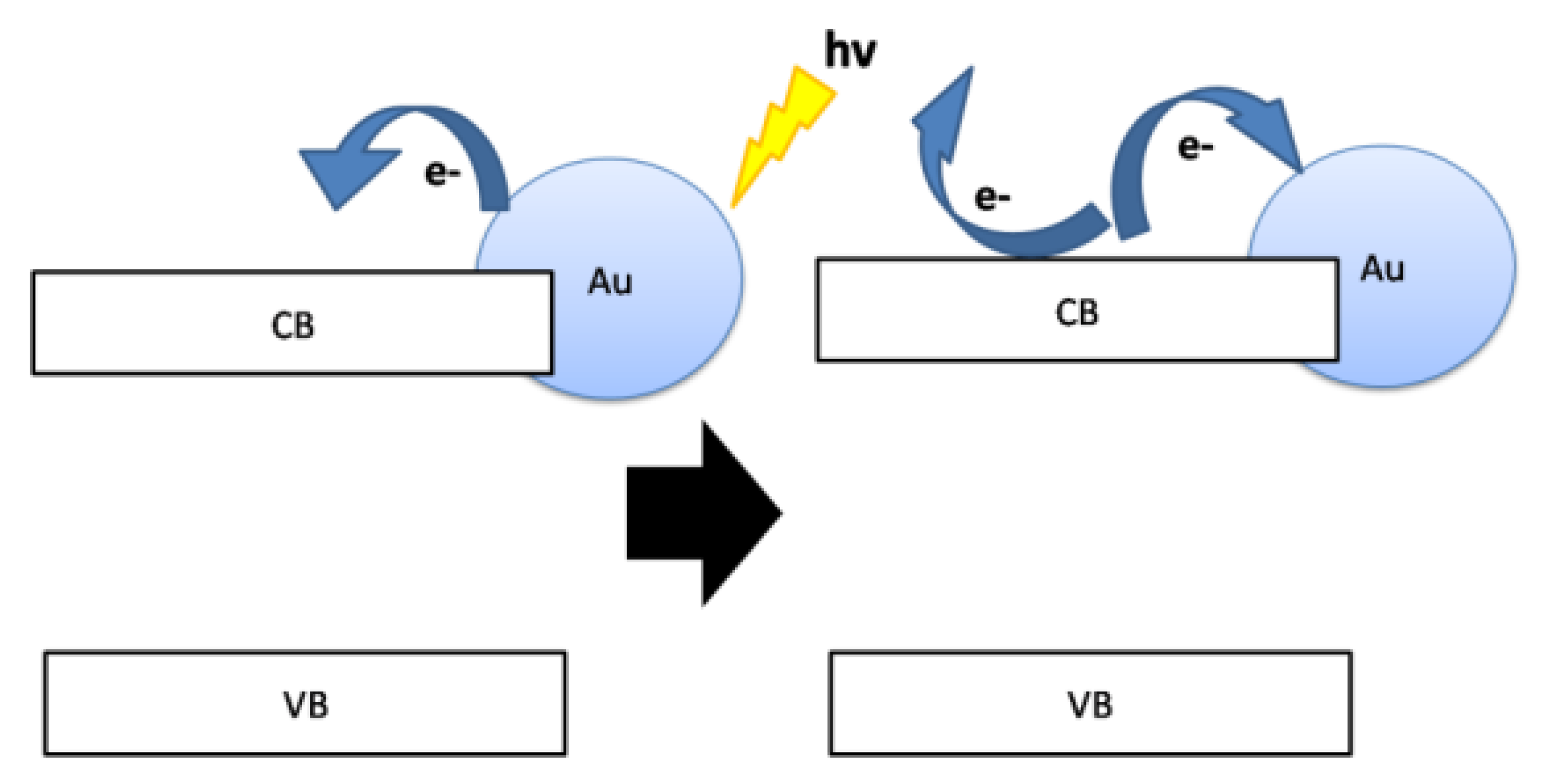
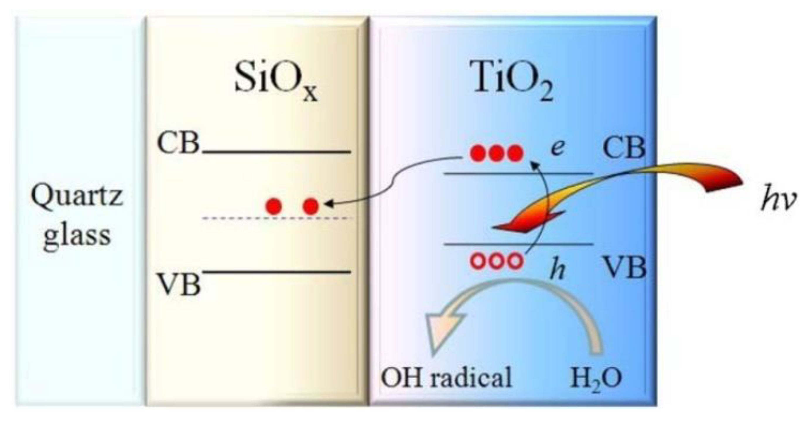
4. Metal Oxide Doping

Many researchers have found that doping metals into TiO2 films enhances their photocatalytic activity and extends the absorption edge into the visible light region [107,133]. Metals can be doped into TiO2 films using layer-by-layer [45,134,135,136] and co-sputtering [57,137] methods. The co-sputtering method allows easy composition control and the layer-by-layer method yields higher quality thin films [136].
TiO2 is an important material for transparent conducting oxide (TCO) layers in thin films because it has high optical transmittance (>80%) in the visible range and low resistivity (10−7Ω·cm−1) [4]. Optical materials based on ITO [51,117] and FTO [52,133] are the most widely used TCO films due to their low resistivity (< 10−4Ω·cm−1) [120]. TCO thin films can be used as substrates for the deposition of TiO2 using sputtering to enhance the effect of electron transfer [51]. However, due to the scarcity and high cost of indium, ITO may not be able to satisfy anticipated demand in the future. Moreover, TiO2 films usually demonstrate poor responses under visible light due to their wide band gap (Eg = 3.20 eV). In order to solve this problem, many researchers have found that metal doping effectively enhances the photoelectric properties [57,94,138] and lowers the band gap of TiO2 films [139]. When the two materials are connected electrically, electrons migrate from the semiconductor to the metal until the two Fermi levels are aligned [17]. Therefore, several dopants, such as Ag [94,125], Al [61], Au [57], CdS, CeO [109], CeO2 [109], Cr, Cu [135], Fe [18], Mo [132], Nb [140,141], Pt [134], and Si [113], have been used for TiO2 thin film.
Metals such as Cr, Co, and Fe that are deposited on a TiO2 surface can react with oxygen, resulting in the reduction ofTiO2 and the oxidation of the metals [136]. These metals can produce a series change of structure, which affects photocatalytic activity. Liu et al. [62] found that the electron transfer between TiO2 and CeO2 networks via Ti–O–Ce structural units plays an important role in photocatalysis. The results revealed that the CeO1.62TiO2 phase is the original cause of visible light photocatalysis [121]. The holes drifting from CeO1.62TiO2 to TiO2 under an inner electric field can inject photo-induced holes into TiO2 and endow the TiO2-CeO2 composite films with photocatalytic properties. Therefore, the TiO2-CeO2 films have better activity than that of pure TiO2 films under UV illumination [121]. Matsuoka et al. [135] indicated that Pt loading in TiO2 films enhances photocatalytic activity; the optimum Pt loading is determined to be 21 µgcm−2. Carneiro et al. [18] found that the absorption edges of Fe-doped TiO2 films shifted to the visible region with increasing concentrations of iron. Fe-doped TiO2 films prepared at a low iron concentration have a better photocatalytic activity than that of pure TiO2 films. In TiO2, the CB consists of Ti 3d atomic orbital. For example, in Fe-doped TiO2, the mixing of Fe 2p state with O 2p state shifts the CB downward and narrows the band-gap energy of the photocatalyst [139]. Fe with different ion forms (Fe2+, Fe3+ and Fe4+) can act as traps for electron hole pairs and consequently inhibit their recombination. However, increasing metal concentration may increase the recombination rate of photo-generated electron-hole due to the metal ion species acting as both electron and hole traps, and thus forming multiple trap sites. If there are too many traps of charge carriers in the bulk of catalyst or on its way to the surface, its apparent mobility may become low and it will likely recombine with its mobile counterpart generated by subsequent photons before it can reach the surface [142]. The schematic diagram of the mechanism is shown in Figure 11 below.
Zhang et al. [104] reported that the absorption edges of Cu-doped samples shifted to the longer wavelength region; however, the optical transmittance of these films decreases abruptly with increasing copper concentration. Subrahmanyam et al. [19] further tested the photocatalytic activity of Ag-modified TiO2 under UV and sunlight. The silver content on the TiO2 surface is between 0.89 and 5.74 at.%. These results demostrated that the maximum photodegradations of rhodamine red molecules are 3.77 at.% and 0.89 at.% with Ag-doped TiO2 film for irradiation at 254 and 352 nm, respectively. This result suggests that the optimum Ag content in TiO2 films, which depends on the irradiation wavelength, is below 5.74 at.%. Similarly, the results of Jung et al. [57] confirmed that increasing the concentrations of Au in TiO2 films can decrease photocatalytic activity. In addition, Seong et al. [143] found that the type of doping metal in TiO2 films is an important factor; the photocatalytic activity of TiO2/SiOx double-layer samples is superior to that of pure TiO2 thin films and the TiO2/SiO2 double layer. Metal dopants can act as recombination centers for photogenerated holes. Therefore, excess mental dopant decreases the photocatalytic activity of TiO2.
The functional mechanism of photocatalytic activity on metal-doped TiO2 has been investigated [133,144]. Lee and Lee [49] employed the RF magnetron sputtering method to prepare TiO2/SiO2/glass thin films for their investigation of the effect of the SiO2 interlayer on the film properties. It is found that the SiO2 interlayer enhances crystallinity and induces a very fine columnar structure that prevents Na+ ion diffusion. For understanding the photochemical process for metal-doped TiO2 films, Zuo [94] has proposed that the surface plasmon resonance (SPR) of the metal dopant increases the absorption wavelength of the films. For instance, the SPR of Ag nanoparticles was centered at around 490 nm for a cluster-like film [145]. The electrons are trapped in individual clusters or islands, and cannot move freely. Sufficient energy (i.e., from irradiation) can excite surface plasmons, leading to absorption. Hence, the increase of the absorption edge on TiO2:Ag film is predictable. Generally, the mechanism of photocatalytic process is initiated when light with energy equal to or greater than the bandgap, incident on the TiO2 valence band that can lead to the generating positive (holes) and negative (electrons) charge carriers on the surface of TiO2 nanoparticle. These photogenerated electron hole pairs causes recombination, become it gets trapped in metastable states between the CB and VB, or react with the organic pollutant adsorbed on the surface of TiO2. These charge carriers initiate reduction and oxidation reactions of electrons and holes, respectively, at the surface of catalyst which in turns leading to the generation of highly reactive agents, such as superoxide and ∙OH hydroxyl radicals, by reacting with dissolved molecular oxygen, surface hydroxyl groups, and adsorbed water molecules. In the case of metal doping, defect levels are created near the CB, while nonmetals induce additional defect levels above the VB, which in turn narrows the bandgap and thus contributes to visible-light photoactivity. In co-doped and multi doped TiO2, electrons can jump either from these defect levels or from VB to the defect impurity level of the metal or to the topmost level of CB of TiO2. Metal ions existing in variable oxidation states can act as trapping centers of electrons, which results in the enhancement in the lifetime of charge carriers, thereby increasing the photocatalytic activity of TiO2.
A surface plasmon is a collection of electrons of the conduction band which oscillates in the interface between conductor and nonconductor or semiconductor and metal oxide or metal, or semiconductor oxide as well [136,146]. Warren et al. [145] has reported in his work that when an electric field (here we consider solar light, visible light or UV light source) is irradiated the metal’s surface plasmon, the density of electron is decreased on one side of the metal while is increased on the another side. This redistribution of the charge carriers inside the surface plasmon’s, creates an electric field inside and outside the metal. The metal is in opposite direction. A series of charge density oscillations will take place with this displacement of electron density which is caused by the coulombic restoring force. This phenomenon of oscillation of charge density and electric field creation are called either surface plasmon resonance (SPR) or localized surface plasmon resonance (LSPR) [147]. According to the mechanism of hot electron and hole present in the SPR, the excitation of the electron from the plasmonic metal because of the SPR effect, which further comes back to the conduction band of TiO2 for reactions of photocatalysis. The study of Tian et al. with Au-doped TiO2 nanocomposites in an electrochemical cell may be used to explain this mechanism [148]. In most of the studies Au, Ag and Cu have been used as plasmonic metals which elicit hot electrons to transfer from the metal to the semiconductor under solar light illumination. The difference stands for the surface plasmon on Au and Ag is that Au resonates under solar light, whereas Ag resonates in the near-UV light region. Electrons can be excited from the noble metals via the SPR mechanism [149,150,151]. Furube et al. [149] discovered that the flow of excited electrons uses the SPR effect from gold nanoparticles to TiO2 nanoparticles using femtosecond transient absorption spectroscopy. Chen et al. [152] reported the number of electrons that obtained sufficient energy to overcome the Schottky barrier via the Fowler Theory. Water oxidation assisted by plasmon using Au-NR–TiO2 electrodes was studied by Nishijima et al. [151] who confirmed that the evolution of O2 and H2O2 from the electrodes in the solution based on the finding of the induction of electron–hole pairs during water oxidation with a stable plasmon. By using a photoelectrochemical cell Chen et al. [152] have also evaluated the mechanism of water splitting over Au-ZnO photoelectrodes under visible light. The possible mechanism of the photocatalytic process and the transfer of hot electrons in Au- doped TiO2 are shown in Figure 12 [153].
Yan et al. [128] hypothesized that the mixing of metals with TiO2 implanted under a lightly doped layer may lead to: (i) the introduction of an upward self-built electric field which could promote charge separation; (ii) an increase in more photogenerated carriers under visible light as the energy gap is curtailed; (iii) the inhibition of charge separation because of a large number of defects; (iv) the intensify of the Schottky barrier between TiO2 and the metal substrate, and thus hindering a charge transfer.
György and Pérez del Pino [154] found that the dopant incorporation leads to the decrease of the crystallites’ average dimensions. Carneiro et al. [18] and Subrahmanyam et al. [19] reported that metals doped into TiO2 films can act as electron traps at the semiconductor interface. Kamisaka et al. [138] suggested that electron-trapping character of metal doped TiO2 films is affected by the crystal phase of TiO2 and the formal charged state of metals. The trapping of charge carriers can decrease the volume recombination rate of (e/h+) pairs and thus increase the lifetime of charge carriers. The process of charge trapping is depicted as follows [84]:
M n + + e cb M ( n 1 ) +
where Mn+ is the metal ion dopant. The energy level of Mn+/M(n−1)+ lies below the CB edge. Thus, the energy level of transition metal ions affects the trapping efficiency.
Seong et al. [143] illustrated the pathway of charged electrons (e) and holes (h+) in TiO2/SiOx thin films (Figure 13).
The CB and VB edges of TiO2 are located within the SiOx bandgap. Under UV irradiation, the electron-hole pairs are initially generated in the TiO2 layer. The generated electrons are accumulated in the CB of TiO2 that are attracted to the trap level of SiOx due to a difference in the work functions of TiO2 and SiOx and thus preventing e/h+ recombination. This may explain why the photoactivity of a dual-layer photocatalyst is the highest among the prepared samples, even though its light absorbance is not the largest [45]. Jung et al. [57] used the co-sputtering method to prepare Au/TiO2 thin films and found that some of the electrons reacted with lattice metal ions (Ti4+) to form Ti3+ defective sites. The formation processes of defective sites on the TiO2 surface can be expressed as:
TiO 2 + hv h vb + + e cb  
e cb + Au Au
Au + Ti 4 + Ti 3 + + Au  
H 2 O ( abs ) + h vb + OH · + H +
Au + h + Au
The Ti3+ sites arise from the Ti4+ sites at which the photogenerated electrons are trapped [144]. A certain number of Ti3+ ions reduce the electron-hole recombination rate and thus enhance photocatalytic activity [113]. Liu et al. [155] proposed that the doped Ag ions convert Ti4+ to Ti3+ by charge compensation. These phenomena can be explained by the defective sites on the TiO2 surface. The electrons react with adsorbed oxygen molecules or surface Ti4+ can generate reactive species O2•− and reactive center surface Ti3+, respectively. The number of recombination centers of inner Ti3+ thus decreases accordingly. In addition, a loaded silver particle can either transfer one electron to an adsorbed oxygen molecule to form O2•− or move to the TiO2 surface Ti4+ to form surface Ti3+. These photochemical reactions explain why the photocatalytic activity of metal-doped TiO2 films is higher than that of regular TiO2 films.
The photocatalytic efficiency of metal-doped TiO2 films seems to depend on the metal particle size, type of metal dopant, fabrication technology, and the hydrophilicity. Many researchers have proved that a large number of small epitaxial deposits on a semiconductor substrate is energetically capable of trapping photoelectrons which might decrease the space distance of charge carriers and increase the probability of the recombination of electrons and holes [147,149,156]. Thus, smaller particles have better photocatalytic activity because the transportation length of the e/h+ pair from the crystal interface to the surface is shorter; and small grains (<40 nm) are more easily achieve charge separation as compared to large grains [147]. Lin and Wu [61] doped Al into TiO2 films using RF sputtering and resulting in a smaller grain size, lower porosity, a higher linear refractive index, a lower stress-optical coefficient, and a higher visible-infrared transmission. However, Zuo [94] reported that Ag doping in TiO2 films increases the FWHM due to large Ag clusters and broader size distribution. Ag nanoparticles are aggregated and form island-like structures. The large number of irregular nanoparticles and the interaction among the densely packed Ag nanoparticles resulted in broader peaks and red-shifts of absorption curves. The type of metal dopant can also influence photocatalytic activity [57,144]. Anpo and Takeuchi [136] have doped various metals into TiO2 films and then examined their effect on the level of red-shift. It is demonstrated that the order of the red-shift efficiency of doped metals is found to be V > Cr >Mn> Fe > Ni. Such a shift allows metal-ion-implanted TiO2 to use the solar irradiation more effectively in the range of 20–30%. Maeda and Watanabe [13] compared the photocatalytic activity of the plasma-enhanced chemical vapor deposition (PECVD) with those of the sol-gel method for fabricating TiO2 films. Experimental results revealed that the grain size of TiO2 films obtained using the PECVD method is almost uniform after annealing at 900 °C, and that these films have a higher photocatalytic activity than that of those obtained using the sol-gel method. It is inferred that the sputtering process can be used to fabricate optimal photocatalytic thin films. Additional studies have demonstrated that the surface of TiO2 becomes highly hydrophilic under UV light irradiation [55,74]. This is attributed to the structural change in the TiO2 surface. Electrons can reduce the Ti4+ cations to the Ti3+ state, and the holes can oxidize the O2 anions, creating oxygen vacancies. Water molecules can occupy these oxygen vacancies, producing adsorbed OH groups, and making the surface hydrophilic [156]. It has been shown that more OH groups can improve the photocatalytic activity and thus the hydrophilicity may improve further the photocatalysis [147,149,150]. Nevertheless, the putative photocatalytic effects of doping various metals into TiO2 films are still controversial [49,141,148]. Moreover, it has been reported that doping suitable amounts of Si and Ag in TiO2 films significantly enhance hydrophilicity [49,147,148]. However, Jun and Lee [141] found that Cr doping is accompanied by the formation of not only the rutile TiO2 phase but also the Cr2O3 phase, all of which degraded hydrophilicity [151,152,153]. The hydrophilicity of films has been evaluated by examining photographs and measuring the contact angle of a water droplet. The water contact angle (θ) can be calculated as [50]:
θ = arctan 4 H L L 2 4 H 2
where L and H are the diameter and height of the spherical crown, respectively.

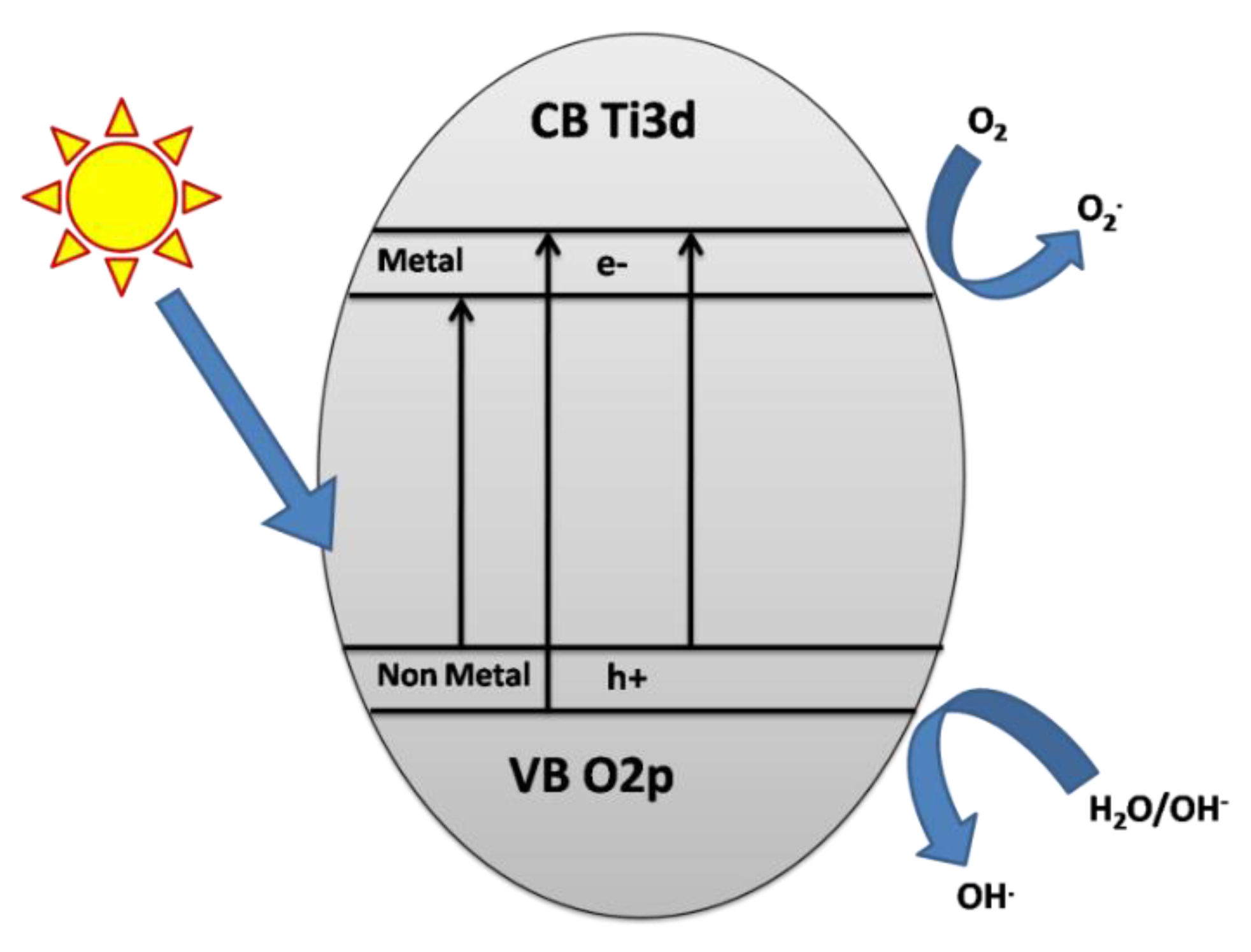
5. Non-Metal Oxide Doping

Doping materials in the TiO2 thin films is a very common approach for enhancement of the TiO2 photocatalytic activity [154,155,157,158,159,160]. The main strategy of the doping is the tailoring of the band gap extending the absorption at longer wavelength. The dopants include transition, noble metals, non-metals and oxide materials as well. Noble metals like Ag, Au, Pd, and Pt exhibits better absorption properties in incorporating with TiO2 followed by the mechanism of surface plasmon resonance (SPR) [161]. TiO2 thin film incorporated with Au and Ag exhibited red-shifted wavelength and boost plasmon resonance, which can improve the overall photocatalytic organic decomposition [162,163]. However, metallic NPs can also enhance the photocatalytic performance of TiO2 thin films through a non-plasmonic mechanism. But they have high cost which limits their usage in doping science with a large scale applications, whereas, transition metals offer more cost-effective processes [164]. On the other hand, non-metals are heavily preferred in the doping of TiO2 thin films. Some of commonly used non-metals dopants are N, B, and S. [165,166]. Other non-metals such as, H, F, and I have also been incorporated into TiO2 thin films during the preparation process to lower the band gap of the composite films to drives it to provide visible light photocatalytic activity. Valentin et al. have employed the density functional theory (DFT) to investigate the effects on the electronic structure of replacing lattice O atoms with B, C, N, or F dopants, or the inclusion of the same atoms in interstitial positions. The energy level of the bands introduced by doping increases with decreasing electronegativity. Fluorine is very electronegative, which introduces states below the O 2p valence band and leads to the formation of Ti3+ ions due to the charge compensation. In case of doping with B and C, this leads to the combination of energy levels above and below the valence band. For further improvement of visible light-driven photocatalysis, binary and ternary co-doping of two nonmetal elements such as N-C and N-B has also been studied. In many cases the synergistic effect is observed for the co-doping, but the parameters used in co-doping are very complex so there is no clear cut conclusion on doping effects [167,168,169,170,171,172].
Non-metal doping into TiO2 thin films has many effects on the microstructure of the material that is depending on the reaction route in spite of band gap narrowing and visible light-driven photocatalysis. B-doped TiO2 shows reduced size with a resulting higher surface area and suppressed phase transformation, and improved photogenerated charge separation, which may contribute to the photocatalysis-enhanced performance of titania [173,174,175,176]. The general mechanism of the doped TiO2 with metal or nonmetal is visualized below (Figure 14):
The doping of nonmetals into TiO2 films leads to great photocatalytic activity [16]. Non-metals used as dopants include nitrogen (N) [171,172], carbon (C) [171], sulfur (S) [144], and fluorine (F) [22]. Many researchers have found that non-metals introduced into TiO2 films can narrow the band gap [156], which is believed to be responsible for increasing the photocatalytic activity at long wavelengths (λ > 500 nm) [171].
Nitrogen can be easily introduced into the TiO2 structure due to its comparable atomic size with that of oxygen, small ionization energy, and high stability. Therefore, nitrogen is the most promising non-metal dopant. Pelaez et al. [16] used various nitrogen-containing organic compounds in a modified sol-gel method to synthesize N-doped TiO2. The obtained samples showed a better photocatalytic activity compared to those of other metal-ion-doped TiO2 samples and Evonik P25-TiO2. Bersani et al. [20] demonstrated that a significantly high substitution of the lattice O atoms of TiO2 with N atoms narrows the band gap of TiO2 thin films, enabling them to absorb and operate under visible light irradiation as a highly reactive, effective photocatalyst. Prabakar et al. [177] prepared visible-light-active nitrogen-doped TiO2 films using DC-reactive magnetron sputtering with a Ti target in an Ar + O2/N gas mixture. These results indicated that increasing the amount of N decreased the particle size of the anatase phase. Moreover, the absorption edge tends to be red-shifted as the N concentrations are increased. Parker and Siegel [178] used Raman spectra to analyze photocatalysts discovered that oxygen deficiency is the origin of all these effects. A clear decrease in the band gap and the nitrogen 2p states on the top of the VB on N-doped TiO2 (compared to those of pure TiO2) has found by Sathish et al. [179]. Di Valentin et al. [180] reported that the Ti–N bond lengths (1.964 and 2.081 Å) are similar to the Ti–O bond lengths (1.942 and 2.002 Å) in the matrix. This infers that N can easily substitute the O sites in the TiO2 structure, and that the change may not degrade the crystallinity. Moreover, Lindgren et al. [181] found that a small concentration of N promotes the growth of anatase. Li and Shang [182] reported that N-doped TiO2 photocatalyst is an anatase-rutile mixed phase which leads to a better electron-hole separation and enhances the visible light photocatalytic activity.
Both carbon and sulfur dopants have shown positive results for visible light activity in TiO2, since they narrow the band gap [16,174]. Hamal and Klabunde [183] indicated that carbon embedded in the TiO2 structure increases visible light absorption, and that carbon can act as a trap site within the CB and the VB, increasing the lifetime of photogenerated charge carriers. Khan et al. [153] prepared carbon-modified rutile TiO2 using flame spray pyrolysis and observed that carbon replaces some of the lattice oxygen sites. Hsu et al. [184] has obtained a similar result, finding that carbon in TiO2 substitutes the lattice oxygen atoms and forms Ti–C bonds. XPS spectra of C-doped TiO2 has revealed a C 1s peak at ~281.8 eV and a free graphitic peak (C–C) at 284.6 eV [182]. The former is regarded as a response to visible light and the latter is served as a photosensitizer [184,185]. Furthermore, carbon doping of TiO2 increases the absorption edge, which can be attributed to the visible light sensitivity originating from the localized C 2p formed in the band gap. Periyat et al. [176] used sulfuric acid to modify TiO2 and found that the anatase phase can resist high temperatures (≥800 °C) and that the presence of sulfur increases visible light photocatalytic activity. The effect of fluorine dopant is similar to that of sulfur dopant in TiO2; it increases the anatase to rutile phase transformation temperature [22]. Fluorine dopant is unable to shift the TiO2 band gap; nevertheless, it improves the surface acidity and causes the formation of reduced Ti3+ ions due to the charge compensation between F and Ti4+ [16]. The present review has identified that nitrogen and carbon are the most suitable non-metals for doping TiO2 films in the sputtering process.

6. Annealing Treatment

It has been demonstrated that annealing treatment provides extra energy for the growth of the crystalline phase of TiO2 films which is similar to the effect of substrate temperature all of which affects the crystalline phases [50,71]. XRD patterns show that the anatase (211) peak increases with an increasing annealing temperature on TiO2 films (Figure 15) [186].
Zhang et al. [104] found that the anatase phase appears when the annealing temperature is higher than 300 °C. Others observed that the rutile phase is first found at annealing temperatures of 600 to 800 °C [12,56,71]. The anatase phase changes into the rutile phase completely at 1000 °C [50], while the brookite phase initially forms at annealing temperatures of above 1000 °C [50].
Zhang et al. [104] also reported that the photocatalytic activity decreases with an increasing in the annealing temperature from 200 to 900 °C. Ye et al. [71] annealed as-deposited TiO2 films at 500 °C and obtained the same result, which is attributed to the reduction of oxygen vacancies on the surface of TiO2; this has implied that a change of elemental composition (Ti3+ changed to Ti4+) on the surface of TiO2 films occurres when the deposited films are annealed, which can decrease the photocatalytic activity on the surface of TiO2 films by increasing the electron-hole recombination rate. However, Meng and Lu [187] have obtained a different result. They found that the photocatalytic activity of TiO2 films annealed at 600 °C is the lowest, and then increases with increasing annealing temperature. The content of anatase TiO2 is gradually decreased while the rutile TiO2 is rather increased. This suggests that the annealing temperature affects the crystalline phase of TiO2 and thus influences its photocatalytic activity.
Annealing treatment also influences the optical properties of TiO2 films. Hasan et al. [72] found that the band gap of annealed films increases with increasing temperature (from 300 to 600 °C). Other optical properties (the extinction coefficient (see Equation (24)), refractive index, and transmittance) are decreased with increasing temperature. Zhang et al. [104] also found that annealing can cause opacity and that transmittance decreases with increasing annealing temperature (200 to 900 °C). Kumar et al. [1] found that annealed films exhibit an enhanced refractive index and a larger band gap, which is ascribed to the improvement in packing density, crystallinity, and decrease in the porosity ratio. These results are indirect evidence that anatase TiO2 transformed into rutile TiO2. Such degraded optical properties after annealing treatment, which may be attributed to higher packing density within the film and a slight increase in crystallinity [1,72].
The extinction coefficient (k) can be derived [37,69] as:
α = 4 π κ λ
where α is the absorption coefficient and λ is the absorption wavelength. A low extinction coefficient implies low absorption [37].
Many studies have demonstrated that the grain size is increased with increasing annealing temperature [15,50,185]. Ye et al. [71] found that increased grain size results in increased density of TiO2 thin films results in increased refractivity, but a decreased porosity ratio (P%). Ye et al. [71] and Hasan et al. [72] reported that P% is decreased with increasing annealing temperature (Figure 16).
A correlation between the photocatalytic activity and porosity has been confirmed by a study that obtained the highest photocatalytic activity is associated with a high-porosity photocatalyst [188].
Regarding hydrophilicity, Ye et al. [71] found that the decrease in water contact angle is associated with increases annealing temperature in the range of 200 to 600 °C, and then is further increased for a higher temperatures above 800 °C (Figure 17).
This result is consistent with those reported by Liu et al. [155] and Meng et al. [50], who concluded that amorphous TiO2 has poor hydrophilicity, anatase TiO2 has excellent hydrophilicity, and rutile TiO2 has good hydrophilicity. The hydrophilicity effect of anatase TiO2 is superior to that of rutile TiO2 which is due to the surface roughness [155,189]. Khadar and Shanid [190] has demonstrated that the surface roughness of TiO2 films is increased with increasing annealing temperature; this phenomenon is due mainly to the ballistic agglomeration vertically on the film.

7. Conclusions

This review demonstrated that TiO2 is a promising semiconductor and photocatalyst due to its physical, structural, and optical properties under UV light. The working principle of the magnetron sputtering is discussed in detail, from which we can examine the process of electron transfer from the cathode to the target substrate material and the effect on sputtering power, pressure, etc. In order to prepare optimal TiO2 films, the sputtering power, working pressure, argon/oxygen ratio, substrate temperature, dopant type, and annealing treatment must be carefully selected. Due to a high surface area, TiO2 nanoparticles exhibit a high photocatalytic activity, nevertheless, their direct use in water treatment application is limited since their recovery from such aqueous medium needs advanced technologies which is very costly. Therefore, there is a need of TiO2 thin films for high photocatalytic activity for both air and water treatments. By tailoring the surface morphology and properties, the photocatalytic activity of TiO2 thin film can be improved in spite of the worse performance than TiO2 nanoparticles. Thus, reactive sputtering systems and evaporation techniques are critical strategies for improving the morphological as well as other properties which can enhance the efficiency of the TiO2 thin films. Optimal TiO2 films must have a small particle size, a strong degree of crystallinity, a low band gap, a low contact angle (hydrophilic), and a high refractive index, transmittance, and extinction coefficient. Metal dopants in TiO2 films can act as electron traps, preventing recombination. The photocatalytic activity of metal-doped TiO2 films is thus higher than that of pure TiO2 films. Non-metal dopants, in particular nitrogen, can substitute sites in the TiO2 lattice. Other non-metal dopants, including carbon, fluorine, and sulfur, have been shown to increase visible light photo-induced activity by retaining the anatase phase of TiO2 films at high temperature. However, only nitrogen and carbon are suitable for the magnetron sputtering process.

Author Contributions

Conceptualization, Y.-H.W., C.-C.W., K.-C.C.; investigation, Y.-H.W., C.-C.W., K.-C.C.; resources, K.-C.C.; writing—original draft preparation, Y.-H.W.; writing—review and editing, Y.-H.W., K.H.R., K.-C.C.; supervision, K.-C.C.; project administration, K.-C.C.; funding acquisition, K.-C.C. All authors have read and agreed to the published version of the manuscript.

Funding

The authors would like to thank the Ministry of Science and Technology (MOST) of Taiwan for financial support under Grant MOST 108-2637-E-020-007.

Conflicts of Interest

The authors declare no conflict of interest.

References

  1. Kumar, T.S.; Bhuyan, R.K.; Pamu, D. Effect of post annealing on structural, optical and dielectric properties of MgTiO3 thin films deposited by RF magnetron sputtering. Appl. Surf. Sci. 2013, 264, 184–190. [Google Scholar] [CrossRef]
  2. Jeong, S.H.; Kim, J.K.; Kim, B.S.; Shim, S.H.; Lee, B.T. Characterization of SiO2 and TiO2 films prepared using RF magnetron sputtering and their application to anti-reflection coating. Vacuum 2004, 76, 507–515. [Google Scholar] [CrossRef]
  3. Hu, W.; Li, L.; Li, G.; Tang, C.; Sun, L. High-quality brookite TiO2 flowers: Synthesis, characterization, and dielectric performance. Cryst. Growth Des. 2009, 9, 3676–3682. [Google Scholar] [CrossRef]
  4. Tighineanu, A.; Ruff, T.; Albu, S.; Hahn, R.; Schmuki, P. Conductivity of TiO2 nanotubes: Influence of annealing time and temperature. Chem. Phys. Lett. 2010, 494, 260–263. [Google Scholar] [CrossRef]
  5. Lee, C.H.; Kim, K.H.; Choi, H.W. Enhancing Efficiency of Dye-Sensitized Solar Cells Using TiO2 Composite Films and RF-Sputtered Passivating Layer. Mol. Cryst. Liq. Cryst. 2012, 567, 9–18. [Google Scholar] [CrossRef]
  6. Pansila, P.; Witit-Anun, N.; Chaiyakun, S. Influence of sputtering power on structure and photocatalyst properties of DC magnetron sputtered TiO2 thin film. Procedia Eng. 2012, 32, 862–867. [Google Scholar] [CrossRef] [Green Version]
  7. Chen, C.; Ma, W.; Zhao, J. Semiconductor-mediated photodegradation of pollutants under visible-light irradiation. Chem. Soc. Rev. 2010, 39, 4206–4219. [Google Scholar] [CrossRef]
  8. Zheng, S.K.; Xiang, G.; Wang, T.M.; Pan, F.; Wang, C.; Hao, W.C. Photocatalytic activity studies of TiO2 thin films prepared by RF magnetron reactive sputtering. Vacuum 2003, 72, 79–84. [Google Scholar] [CrossRef]
  9. Wang, Q.; Zhu, K.; Neale, N.R.; Frank, A.J. Constructing ordered sensitized heterojunctions: Bottom-up electrochemical synthesis of p-type semiconductors in oriented n-TiO2 nanotube arrays. Nano Lett. 2009, 9, 806–813. [Google Scholar] [CrossRef]
  10. Hanaor, D.A.; Sorrell, C.C. Review of the anatase to rutile phase transformation. J. Mater. Sci. 2011, 46, 855–874. [Google Scholar] [CrossRef] [Green Version]
  11. Yang, Z.; Choi, D.; Kerisit, S.; Rosso, K.M.; Wang, D.; Zhang, J.; Graff, G.; Liu, J. Nanostructures and lithium electrochemical reactivity of lithium titanites and titanium oxides: A review. J. Power Sour. 2009, 192, 588–598. [Google Scholar] [CrossRef]
  12. Yoo, D.; Kim, I.; Kim, S.; Hahn, C.H.; Lee, C.; Cho, S. Effects of annealing temperature and method on structural and optical properties of TiO2 films prepared by RF magnetron sputtering at room temperature. Appl. Surf. Sci. 2007, 253, 3888–3892. [Google Scholar] [CrossRef]
  13. Maeda, M.; Watanabe, T. Effects of crystallinity and grain size on photocatalytic activity of titania films. Surf. Coat. Technol. 2007, 201, 9309–9312. [Google Scholar] [CrossRef]
  14. Takabayashi, S.; Zeman, P. Effect of total and oxygen partial pressures on structure of photocatalytic TiO2 films sputtered on unheated substrates. Surf. Coat. Technol. 2002, 153, 93–99. [Google Scholar]
  15. Ogawa, H.; Higuchi, T.; Nakamura, A.; Tokita, S.; Miyazaki, D.; Hattori, T.; Tsukamoto, T. Growth of TiO2 thin film by reactive RF magnetron sputtering using oxygen radical. J. Alloys Compd. 2008, 449, 375–378. [Google Scholar] [CrossRef]
  16. Pelaez, M.; Nolan, N.T.; Pillai, S.C.; Seery, M.K.; Falaras, P.; Kontos, A.G.; Dunlop, P.S.; Hamilton, J.W.; Byrne, J.A.O.; Shea, K.; et al. A review on the visible light active titanium dioxide photocatalysts for environmental applications. Appl. Catal. B 2012, 125, 331–349. [Google Scholar] [CrossRef] [Green Version]
  17. Herrmann, J.M. Heterogeneous photocatalysis: State of the art and present applications In honor of Pr. RL Burwell Jr. (1912–2003), Former Head of Ipatieff Laboratories, Northwestern University, Evanston (Ill). Top. Catal. 2005, 34, 49–65. [Google Scholar] [CrossRef]
  18. Carneiro, J.O.; Teixeira, V.; Portinha, A.; Dupak, L.; Magalhaes, A.; Coutinho, P. Study of the deposition parameters and Fe-dopant effect in the photocatalytic activity of TiO2 films prepared by dc reactive magnetron sputtering. Vacuum 2005, 78, 37–46. [Google Scholar] [CrossRef]
  19. Subrahmanyam, A.; Biju, K.P.; Rajesh, P.; Kumar, K.J.; Kiran, M.R. Surface modification of sol gel TiO2 surface with sputtered metallic silver for Sun light photocatalytic activity: Initial studies. Sol. Energy Mater. Sol. Cell 2012, 101, 241–248. [Google Scholar] [CrossRef]
  20. Bersani, D.; Lottici, P.P.; Ding, X.Z. Phonon confinement effects in the Raman scattering by TiO2 nanocrystals. Appl. Phys. Lett. 1998, 72, 73–75. [Google Scholar] [CrossRef]
  21. Lee, S.H.; Yamasue, E.; Okumura, H.; Ishihara, K.N. Effect of oxygen and nitrogen concentration of nitrogen doped TiOx film as photocatalyst prepared by reactive sputtering. Appl. Catal. A-Gen. 2009, 371, 179–190. [Google Scholar] [CrossRef]
  22. Padmanabhan, S.C.; Pillai, S.C.; Colreavy, J.; Balakrishnan, S.; McCormack, D.E.; Perova, T.S.; Gun’ko, Y.; Hinder, S.J.; Kelly, J.M. A simple sol− gel processing for the development of high-temperature stable photoactive anatase titania. Chem. Mater. 2007, 19, 4474–4481. [Google Scholar] [CrossRef]
  23. Wiatrowski, A.; Mazur, M.; Obstarczyk, A.; Wojcieszak, D.; Kaczmarek, D.; Morgiel, J.; Gibson, D. Comparison of the physicochemical properties of TiO2 thin films obtained by magnetron sputtering with continuous and pulsed gas flow. Coatings 2018, 8, 412. [Google Scholar] [CrossRef] [Green Version]
  24. Veith, M.; Lee, J.; Miró, M.M.; Akkan, C.K.; Dufloux, C.; Aktas, O.C. Bi-phasic nanostructures for functional applications. Chem. Soc. Rev. 2012, 41, 5117–5130. [Google Scholar] [CrossRef] [PubMed]
  25. Su, J.; Boichot, R.; Blanquet, E.; Mercier, F.; Pons, M. Chemical vapor deposition of titanium nitride thin films: Kinetics and experiments. Cryst. Eng. Comm. 2019, 21, 3974–3981. [Google Scholar] [CrossRef]
  26. Henkel, B.; Neubert, T.; Zabel, S.; Lamprecht, C.; Selhuber-Unkel, C.; Raetzke, K.; Strunskus, T.; Vergöhl, M.; Faupel, F. Photocatalytic properties of titania thin films prepared by sputtering versus evaporation and aging of induced oxygen vacancy defects. Appl. Catal. B 2016, 180, 362–371. [Google Scholar] [CrossRef]
  27. Rodríguez, J.; Gómez, M.; Lu, J.; Olsson, E.; Granqvist, C.G. Reactively Sputter-Deposited Titanium Oxide Coatings with Parallel Penniform Microstructure. Adv. Mater. 2000, 12, 341–343. [Google Scholar] [CrossRef]
  28. Suzuki, M.; Ito, T.; Taga, Y. Photocatalysis of sculptured thin films of TiO2. Appl. Phys. Lett. 2001, 78, 3968–3970. [Google Scholar] [CrossRef]
  29. Merenda, A.; Kong, L.; Zhu, B.; Duke, M.C.; Gray, S.R.; Dumée, L.F. Functional nanoporous titanium dioxide for separation applications: Synthesis routes and properties to performance analysis. In Water Scarcity and Ways to Reduce the Impact; Springer: Cham, Switzerland, 2019; pp. 151–186. [Google Scholar]
  30. Henkel, B.; Vahl, A.; Aktas, O.C.; Strunskus, T.; Faupel, F. Self-organized nanocrack networks: A pathway to enlarge catalytic surface area in sputtered ceramic thin films, showcased for photocatalytic TiO2. Nanotechnology 2017, 29, 035703. [Google Scholar] [CrossRef]
  31. Mejia, M.I.; Marin, J.M.; Restrepo, G.; Pulgarin, C.; Mielczarski, E.; Mielczarski, J.; Arroyo, Y.; Lavanchy, J.C.; Kiwi, J. Self-cleaning modified TiO2–cotton pretreated by UVC-light (185 nm) and RF-plasma in vacuum and also under atmospheric pressure. Appl. Catal. B 2009, 91, 481–488. [Google Scholar] [CrossRef]
  32. Chen, D.Y.; Tsao, C.C.; Hsu, C.Y. Photocatalytic TiO2 thin films deposited on flexible substrates by radio frequency (RF) reactive magnetron sputtering. Curr. Appl. Phys. 2012, 12, 179–183. [Google Scholar] [CrossRef]
  33. Chiou, A.H.; Kuo, C.G.; Huang, C.H.; Wu, W.F.; Chou, C.P.; Hsu, C.Y. Influence of oxygen flow rate on photocatalytic TiO2 films deposited by rf magnetron sputtering. J. Mater. Sci.-Mater. Electron. 2012, 23, 589–594. [Google Scholar] [CrossRef] [Green Version]
  34. Wei, C.H.; Chang, C.M. Polycrystalline TiO2 thin films with different thicknesses deposited on unheated substrates using RF magnetron sputtering. Mater. Trans. 2011. [Google Scholar] [CrossRef] [Green Version]
  35. Yang, W.; Liu, Z.; Peng, D.L.; Zhang, F.; Huang, H.; Xie, Y.; Wu, Z. Room-temperature deposition of transparent conducting Al-doped ZnO films by RF magnetron sputtering method. Appl. Surf. Sci. 2009, 255, 5669–5673. [Google Scholar] [CrossRef]
  36. Nair, P.B.; Justinvictor, V.B.; Daniel, G.P.; Joy, K.; Ramakrishnan, V.; Thomas, P.V. Effect of RF power and sputtering pressure on the structural and optical properties of TiO2 thin films prepared by RF magnetron sputtering. Appl. Surf. Sci. 2011, 257, 10869–10875. [Google Scholar] [CrossRef]
  37. Laha, P.; Panda, A.B.; Mahapatra, S.K.; Barhai, P.K.; Das, A.K.; Banerjee, I. Development of RF plasma sputtered Al2O3–TiO2 multilayer broad band antireflecting coatings and its correlation with plasma parameters. Appl. Surf. Sci. 2012, 258, 2275–2282. [Google Scholar] [CrossRef]
  38. Shet, S.; Ahn, K.S.; Nuggehalli, R.; Yan, Y.; Turner, J.; Al-Jassim, M. Effects of substrate temperature and RF power on the formation of aligned nanorods in ZnO thin films. JOM-US 2010, 62, 25–30. [Google Scholar] [CrossRef]
  39. Jamuna-Thevi, K.; Bakar, S.A.; Ibrahim, S.; Shahab, N.; Toff, M.R. Quantification of silver ion release, in vitro cytotoxicity and antibacterial properties of nanostuctured Ag doped TiO2 coatings on stainless steel deposited by RF magnetron sputtering. Vacuum 2011, 86, 235–241. [Google Scholar] [CrossRef]
  40. Sun, H.; Wang, C.; Pang, S.; Li, X.; Tao, Y.; Tang, H.; Liu, M. Photocatalytic TiO2 films prepared by chemical vapor deposition at atmosphere pressure. J. Non-Cryst. Solids 2008, 354, 1440–1443. [Google Scholar] [CrossRef]
  41. Amadelli, R.; Samiolo, L.; Maldotti, A.; Molinari, A.; Valigi, M.; Gazzoli, D. Preparation, characterisation, and photocatalytic behaviour of Co-TiO2 with visible light response. Int. J. Photoenergy 2008, 2008, 853753. [Google Scholar] [CrossRef] [Green Version]
  42. Lei, Y.; Zhang, L.D.; Fan, J.C. Fabrication, characterization and Raman study of TiO2 nanowire arrays prepared by anodic oxidative hydrolysis of TiCl3. Chem. Phys. Lett. 2001, 338, 231–236. [Google Scholar] [CrossRef]
  43. Arconada, N.; Castro, Y.; Durán, A. Photocatalytic properties in aqueous solution of porous TiO2-anatase films prepared by sol–gel process. Appl. Catal. A-Gen. 2010, 385, 101–107. [Google Scholar] [CrossRef]
  44. Khoa, N.T.; Pyun, M.W.; Yoo, D.H.; Kim, S.W.; Leem, J.Y.; Kim, E.J.; Hahn, S.H. Photodecomposition effects of graphene oxide coated on TiO2 thin film prepared by electron-beam evaporation method. Thin Solid Films 2012, 520, 5417–5420. [Google Scholar] [CrossRef]
  45. Liao, C.H.; Huang, C.W.; Wu, J.C. Novel dual-layer photoelectrode prepared by RF magnetron sputtering for photocatalytic water splitting. Int. J. Hydrog. Energy 2012, 37, 11632–11639. [Google Scholar] [CrossRef]
  46. Yang, W.J.; Hsu, C.Y.; Liu, Y.W.; Hsu, R.Q.; Lu, T.W.; Hu, C.C. The structure and photocatalytic activity of TiO2 thin films deposited by dc magnetron sputtering. Superlattice Microstruct. 2012, 52, 1131–1142. [Google Scholar] [CrossRef]
  47. Garlisi, C.; Scandura, G.; Palmisano, G.; Chiesa, M.; Lai, C.Y. Integrated nano-and macroscale investigation of photoinduced hydrophilicity in TiO2 thin films. Langmuir 2016, 32, 11813–11818. [Google Scholar] [CrossRef]
  48. Haseeb, A.S.; Hasan, M.M.; Masjuki, H.H. Structural and mechanical properties of nanostructured TiO2 thin films deposited by RF sputtering. Surf. Coat. Technol. 2010, 205, 338–344. [Google Scholar] [CrossRef]
  49. Lee, K.S.; Lee, S.H. Influence of SiO2 interlayer on the hydrophilicity of TiO2/SiO2/glass produced by RF-magnetron sputtering. Mater. Lett. 2007, 61, 3516–3518. [Google Scholar] [CrossRef]
  50. Meng, F.; Xiao, L.; Sun, Z. Thermo-induced hydrophilicity of nano-TiO2 thin films prepared by RF magnetron sputtering. J. Alloys Compd. 2009, 485, 848–852. [Google Scholar] [CrossRef]
  51. Ohsaki, H.; Andou, R.; Kinbara, A.; Watanabe, T. Crystallization of ITO and TiO2 by RF plasma treatment. Vacuum 2013, 87, 145–149. [Google Scholar] [CrossRef]
  52. Choi, W.J.; Kwak, D.J.; Park, C.S.; Sung, Y.M. Characterization of transparent conductive ITO, ITiO, and FTO Films for application in photoelectrochemical cells. J. Nanosci. Nanotechnol. 2012, 12, 3394–3397. [Google Scholar] [CrossRef] [PubMed]
  53. Song, S.; Yang, T.; Li, Y.; Pang, Z.; Lin, L.; Lv, M.; Han, S. Structural, electrical and optical properties of ITO films with a thin TiO2 seed layer prepared by RF magnetron sputtering. Vacuum 2009, 83, 1091–1094. [Google Scholar] [CrossRef]
  54. Rhee, S.W.; Kim, K.H.; Choi, H.W. Effect of ZnO Passivating Layer Using RF-Sputtered for Dye-Sensitized Solar Cells. Mol. Cryst. Liq. Cryst. 2012, 565, 131–137. [Google Scholar] [CrossRef]
  55. Chen, C.C.; Yang, W.J.; Hsu, C.Y. Investigation into the effects of deposition parameters on TiO2 photocatalyst thin films by rf magnetron sputtering. Superlattice Microstruct. 2009, 46, 461–468. [Google Scholar] [CrossRef]
  56. Wenbin, X.; Shurong, D.; Demiao, W.; Gaochao, R. Investigation of microstructure evolution in Pt-doped TiO2 thin films deposited by RF magnetron sputtering. Physica B 2008, 403, 2698–2701. [Google Scholar] [CrossRef]
  57. Jung, J.M.; Wang, M.; Kim, E.J.; Hahn, S.H. Photocatalytic properties of Au/TiO2 thin films prepared by RF magnetron co-sputtering. Vacuum 2008, 82, 827–832. [Google Scholar] [CrossRef]
  58. Lin, S.S. The optical properties of Ti-doped TiO2 nanoceramic films deposited by simultaneous RF and DC magnetron sputtering. Ceram. Int. 2012, 38, 3129–3134. [Google Scholar] [CrossRef]
  59. Huang, H.H.; Huang, C.C.; Huang, P.C.; Yang, C.F.; Hsu, C.Y. Preparation of rutile and anatase phases titanium oxide film by RF sputtering. J. Nanosci. Nanotechnol. 2008, 8, 2659–2664. [Google Scholar] [CrossRef]
  60. Su, Y.F.; Chou, T.C.; Ling, T.R.; Sun, C.C. Photocurrent performance and nanostructure analysis of TiO2/ITO electrodes prepared using reactive sputtering. J. Electrochem. Soc. 2004, 151, A1375–A1382. [Google Scholar] [CrossRef] [Green Version]
  61. Lin, S.S.; Wu, D.K. Effect of RF deposition power on the properties of Al-doped TiO2 thin films. Surf. Coat. Technol. 2010, 204, 2202–2207. [Google Scholar] [CrossRef]
  62. Liu, B.; Zhao, X.; Zhao, Q.; Li, C.; He, X. The effect of O2 partial pressure on the structure and photocatalytic property of TiO2 films prepared by sputtering. Mater. Chem. Phys. 2005, 90, 207–212. [Google Scholar] [CrossRef]
  63. Magyari-Köpe, B.; Park, S.G.; Lee, H.D.; Nishi, Y. First principles calculations of oxygen vacancy-ordering effects in resistance change memory materials incorporating binary transition metal oxides. J. Mater. Sci. 2012, 47, 7498–7514. [Google Scholar] [CrossRef]
  64. Sirisuk, A.; Klansorn, E.; Praserthdam, P. Effects of reaction medium and crystallite size on Ti3+ surface defects in titanium dioxide nanoparticles prepared by solvothermal method. Catal. Commun. 2008, 9, 1810–1814. [Google Scholar] [CrossRef]
  65. Chow, L.L.; Yuen, M.M.; Chan, P.C.; Cheung, A.T. Reactive sputtered TiO2 thin film humidity sensor with negative substrate bias. Sens. Actuators B-Chem. 2001, 76, 310–315. [Google Scholar] [CrossRef]
  66. Huang, C.H.; Tsao, C.C.; Hsu, C.Y. Study on the photocatalytic activities of TiO2 films prepared by reactive RF sputtering. Ceram. Int. 2011, 37, 2781–2788. [Google Scholar] [CrossRef]
  67. Eufinger, K.; Poelman, D.; Poelman, H.; De Gryse, R.; Marin, G.B. Photocatalytic activity of dc magnetron sputter deposited amorphous TiO2 thin films. Appl. Surf. Sci. 2007, 254, 148–152. [Google Scholar] [CrossRef]
  68. Hou, Y.Q.; Zhuang, D.M.; Zhang, G.; Zhao, M.; Wu, M.S. Influence of annealing temperature on the properties of titanium oxide thin film. Appl. Surf. Sci. 2003, 218, 98–106. [Google Scholar] [CrossRef]
  69. Miao, L.; Jin, P.; Kaneko, K.; Terai, A.; Nabatova-Gabain, N.; Tanemura, S. Preparation and characterization of polycrystalline anatase and rutile TiO2 thin films by rf magnetron sputtering. Appl. Surf. Sci. 2003, 212, 255–263. [Google Scholar] [CrossRef]
  70. Zhang, T.J.; Li, S.Z.; Zhang, B.S.; Pan, R.K.; Jiang, J.; Ma, Z.J. Optical properties of RF-sputtered Ba0.65Sr0.35TiO3 thin films. J. Electroceram. 2008, 21, 174–177. [Google Scholar] [CrossRef]
  71. Ye, Q.; Liu, P.Y.; Tang, Z.F.; Zhai, L. Hydrophilic properties of nano-TiO2 thin films deposited by RF magnetron sputtering. Vacuum 2007, 81, 627–631. [Google Scholar] [CrossRef]
  72. Hasan, M.M.; Haseeb, A.S.; Saidur, R.; Masjuki, H.H.; Hamdi, M. Influence of substrate and annealing temperatures on optical properties of RF-sputtered TiO2 thin films. Opt. Mater. 2010, 32, 690–695. [Google Scholar] [CrossRef]
  73. Heo, C.H.; Lee, S.B.; Boo, J.H. Deposition of TiO2 thin films using RF magnetron sputtering method and study of their surface characteristics. Thin Solid Films 2005, 475, 183–188. [Google Scholar] [CrossRef]
  74. Lin, W.S.; Huang, C.H.; Yang, W.J.; Hsu, C.Y.; Hou, K.H. Photocatalytic TiO2 films deposited by RF magnetron sputtering at different oxygen partial pressure. Curr. Appl. Phys. 2010, 10, 1461–1466. [Google Scholar] [CrossRef]
  75. Kang, S.H.; Lim, J.W.; Kim, H.S.; Kim, J.Y.; Chung, Y.H.; Sung, Y.E. Photo and electrochemical characteristics dependent on the phase ratio of nanocolumnar structured TiO2 films by RF magnetron sputtering technique. Chem. Mater. 2009, 21, 2777–2788. [Google Scholar] [CrossRef]
  76. Zhao, X.T.; Sakka, K.; Kihara, N.; Takata, Y.; Arita, M.; Masuda, M. Hydrophilicity of TiO2 thin films obtained by RF magnetron sputtering deposition. Curr. Appl. Phys. 2006, 6, 931–933. [Google Scholar] [CrossRef]
  77. Song, P.K.; Yamagishi, M.; Odaka, H.; Shigesato, Y. Photoinduced hydrophilicity of epitaxially grown TiO2 films by RF magnetron sputtering. Jpn. J. Appl. Phys. 2003, 42, L1529. [Google Scholar] [CrossRef]
  78. Shibata, A.; Okimura, K.; Yamamoto, Y.; Matubara, K. Effect of heating probe on reactively sputtered TiO2 film growth. Jpn. J. Appl. Phys. 1993, 32, 5666. [Google Scholar] [CrossRef]
  79. Kasemanankul, P.; Witit-Anan, N.; Chaiyakun, S.; Limsuwan, P.; Boonamnuayvitaya, V. Low-temperature deposition of (1 1 0) and (1 0 1) rutile TiO2 thin films using dual cathode DC unbalanced magnetron sputtering for inducing hydroxyapatite. Mater. Chem. Phys. 2009, 117, 288–293. [Google Scholar] [CrossRef]
  80. Ngaruiya, J.M.; Kappertz, O.; Mohamed, S.H.; Wuttig, M. Structure formation upon reactive direct current magnetron sputteringof transition metal oxide films. Appl. Phys. Lett. 2004, 85, 748–750. [Google Scholar] [CrossRef]
  81. Sundaram, K.B.; Khan, A. Characterization and optimization of zinc oxide films by RF magnetron sputtering. Thin Solid Films 1997, 295, 87–91. [Google Scholar] [CrossRef]
  82. Barnes, M.C.; Gerson, A.R.; Kumar, S.; Hwang, N.M. The mechanism of TiO2 deposition by direct current magnetron reactive sputtering. Thin Solid Films 2004, 446, 29–36. [Google Scholar] [CrossRef]
  83. Barnes, M.C.; Kim, D.Y.; Ahn, H.S.; Lee, C.O.; Hwang, N.M. Deposition mechanism of gold by thermal evaporation: Approach by charged cluster model. J. Cryst. Growth 2000, 213, 83–92. [Google Scholar] [CrossRef]
  84. Shah, S.I.; Li, W.; Huang, C.P.; Jung, O.; Ni, C. Study of Nd3+, Pd2+, Pt4+, and Fe3+ dopant effect on photoreactivity of TiO2 nanoparticles. Proc. Natl. Acad. Sci. USA 2002, 99 (Suppl. 2), 6482–6486. [Google Scholar] [CrossRef] [Green Version]
  85. Lin, W.S.; Kao, L.M.; Li, W.P.; Hsu, C.Y.; Hou, K.H. Fabricating TiO2 photocatalysts by RF reactive magnetron sputtering at varied oxygen partial pressures. J. Mater. Eng. Perform. 2011, 20, 1063–1067. [Google Scholar] [CrossRef]
  86. Xu, Y.; Shen, M. Fabrication of anatase-type TiO2 films by reactive pulsed laser deposition for photocatalyst application. J. Mater. Process. Technol. 2008, 202, 301–306. [Google Scholar] [CrossRef]
  87. Chaoumead, A.; Joo, B.H.; Kwak, D.J.; Sung, Y.M. Structural and electrical properties of sputtering power and gas pressure on Ti-dope In2O3 transparent conductive films by RF magnetron sputtering. Appl. Surf. Sci. 2013, 275, 227–232. [Google Scholar] [CrossRef]
  88. Jin, Y.S.; Kim, K.H.; Kim, W.J.; Jang, K.U.; Choi, H.W. The effect of RF-sputtered TiO2 passivating layer on the performance of dye sensitized solar cells. Ceram. Int. 2012, 38. S505–S509. [Google Scholar] [CrossRef]
  89. Wang, T.M.; Zheng, S.K.; Hao, W.C.; Wang, C. Studies on photocatalytic activity and transmittance spectra of TiO2 thin films prepared by rf magnetron sputtering method. Surf. Coat. Technol. 2002, 155, 141–145. [Google Scholar] [CrossRef]
  90. Choi, Y.L.; Kim, S.H.; Song, Y.S.; Lee, D.Y. Photodecomposition and bactericidal effects of TiO2 thin films prepared by a magnetron sputtering. J. Mater. Sci. 2004, 39, 5695–5699. [Google Scholar] [CrossRef]
  91. Zhu, H.; Hüpkes, J.; Bunte, E.; Gerber, A.; Huang, S.M. Influence of working pressure on ZnO: Al films from tube targets for silicon thin film solar cells. Thin Solid Films 2010, 518, 4997–5002. [Google Scholar] [CrossRef]
  92. Drüsedau, T.P.; Löhmann, M.; Garke, B. Decay length of the pressure dependent deposition rate for magnetron sputtering. J. Vac. Sci. Technol. A 1998, 16, 2728–2732. [Google Scholar] [CrossRef]
  93. Zhang, C.; Ding, W.; Wang, H.; Chai, W.; Ju, D. Influences of working pressure on properties for TiO2 films deposited by DC pulse magnetron sputtering. J. Environ. Sci. 2009, 21, 741–744. [Google Scholar] [CrossRef]
  94. Zuo, J. Deposition of Ag nanostructures on TiO2 thin films by RF magnetron sputtering. Appl. Surf. Sci. 2010, 256, 7096–7101. [Google Scholar] [CrossRef]
  95. Barreca, D.; Gasparotto, A.; Tondello, E.; Bruno, G.; Losurdo, M. Influence of process parameters on the morphology of Au/SiO2 nanocomposites synthesized by radio-frequency sputtering. J. Appl. Phys. 2004, 96, 1655–1665. [Google Scholar] [CrossRef]
  96. Okimura, K.; Shibata, A. Mass and Energy Analyses of Substrate-incident Ions in TiO2 Deposition by RF Magnetron Sputtering. Jpn. J. Appl. Phys. 1997, 36, 313. [Google Scholar] [CrossRef]
  97. Šícha, J.; Musil, J.; Meissner, M.; Čerstvý, R. Nanostructure of photocatalytic TiO2 films sputtered at temperatures below 200 C. Appl. Surf. Sci. 2008, 254, 3793–3800. [Google Scholar] [CrossRef]
  98. El Akkad, F.; Paulose, T.A. Optical transitions and point defects in F: SnO2 films: Effect of annealing. Appl. Surf. Sci. 2014, 295, 8–17. [Google Scholar] [CrossRef]
  99. Mardare, D.; Tasca, M.; Delibas, M.; Rusu, G.I. On the structural properties and optical transmittance of TiO2 RF sputtered thin films. Appl. Surf. Sci. 2000, 156, 200–206. [Google Scholar] [CrossRef]
  100. Vorontsov, A.V.; Savinov, E.N.; Zhensheng, J. Influence of the form of photodeposited platinum on titania upon its photocatalytic activity in CO and acetone oxidation. J. Photochem. Photobiol. A 1999, 125, 113–117. [Google Scholar] [CrossRef]
  101. Zhang, W.; Li, Y.; Zhu, S.; Wang, F. Influence of argon flow rate on TiO2 photocatalyst film deposited by DC reactive magnetron sputtering. Surf. Coat. Technol. 2004, 182, 192–198. [Google Scholar] [CrossRef]
  102. Tomaszewski, H.; Poelman, H.; Depla, D.; Poelman, D.; De Gryse, R.; Fiermans, L.; Reyniers, M.F.; Heynderickx, G.; Marin, G.B. TiO2 films prepared by DC magnetron sputtering from ceramic targets. Vacuum 2002, 68, 31–38. [Google Scholar] [CrossRef]
  103. Huang, C.L.; Hsu, C.H. Properties of reactively radio frequency-magnetron sputtered (Zr, Sn) TiO4 dielectric films. J. Appl. Phys. 2004, 96, 1186–1191. [Google Scholar] [CrossRef]
  104. Zhang, W.J.; Zhu, S.L.; Li, Y.; Wang, F.H. Photocatalytic property of TiO2 films deposited by pulsed DC magnetron sputtering. J. Mater. Sci. Technol. 2004, 20, 31–34. [Google Scholar]
  105. Pradhan, S.S.; Pradhan, S.K.; Bhavanasi, V.; Sahoo, S.; Sarangi, S.N.; Anwar, S.; Barhai, P.K. Low temperature stabilized rutile phase TiO2 films grown by sputtering. Thin Solid Films 2012, 520, 1809–1813. [Google Scholar] [CrossRef]
  106. Water, W.; Chu, S.Y. Physical and structural properties of ZnO sputtered films. Mater. Lett. 2002, 55, 67–72. [Google Scholar] [CrossRef]
  107. Toku, H.; Pessoa, R.S.; Maciel, H.S.; Massi, M.; Mengui, U.A. The effect of oxygen concentration on the low temperature deposition of TiO2 thin films. Surf. Coat. Technol. 2008, 202, 2126–2131. [Google Scholar] [CrossRef]
  108. Jeong, S.H.; Kim, B.S.; Lee, B.T.; Kim, J.K.; Park, H.R. Structural and optical properties of TiO2 films prepared using reactive RF magnetron sputtering. J. Korean Phys. Soc. 2002, 41, 67–71. [Google Scholar]
  109. Tavares, C.J.; Vieira, J.; Rebouta, L.; Hungerford, G.; Coutinho, P.; Teixeira, V.; Carneiro, J.O.; Fernandes, A.J. Reactive sputtering deposition of photocatalytic TiO2 thin films on glass substrates. Mater. Sci. Eng. B 2007, 138, 139–143. [Google Scholar] [CrossRef]
  110. Xiong, J.; Das, S.N.; Kim, S.; Lim, J.; Choi, H.; Myoung, J.M. Photo-induced hydrophilic properties of reactive RF magnetron sputtered TiO2 thin films. Surf. Coat. Technol. 2010, 204, 3436–3442. [Google Scholar] [CrossRef]
  111. Rahman, K.H.; Kar, A.K. Effect of precursor concentration of microstructured titanium-di-oxide (TiO2) thin films and their photocatalytic activity. Mater. Res. Express 2019, 6, 096436. [Google Scholar] [CrossRef]
  112. Tondare, R.S.; Shivaraj, B.W.; Narasimhamurthy, H.N.; Krishna, M.; Subramanyam, T.K. Effect of deposition time on structural, electrical and optical properties of Aluminium doped ZnO thin films by RF magnetron sputtering. Mater. Today-Proc. 2018, 5, 2710–2715. [Google Scholar] [CrossRef]
  113. Abdallah, B.; Jazmati, A.K.; Refaai, R. Oxygen effect on structural and optical properties of ZnO thin films deposited by RF magnetron sputtering. Mater. Res. 2017, 20, 607–612. [Google Scholar] [CrossRef]
  114. Nakajima, A.; Hashimoto, K.; Watanabe, T.; Takai, K.; Yamauchi, G.; Fujishima, A. Transparent superhydrophobic thin films with self-cleaning properties. Langmuir 2000, 16, 7044–7047. [Google Scholar] [CrossRef]
  115. Vancoppenolle, V.; Jouan, P.Y.; Wautelet, M.; Dauchot, J.P.; Hecq, M. Dc magnetron sputtering deposition of TiO2 films in argon–oxygen gas mixtures: Theory and experiments. Surf. Coat. Technol. 1999, 116, 933–937. [Google Scholar] [CrossRef]
  116. Alnama, K.; Abdallah, B.; Kanaan, S. Deposition of ZnS thin film by ultrasonic spray pyrolysis: Effect of thickness on the crystallographic and electrical properties. Compos. Interface 2017, 24, 499–513. [Google Scholar] [CrossRef]
  117. Abdallah, B.; Ismail, A.; Kashoua, H.; Zetoun, W. Effects of deposition time on the morphology, structure, and optical properties of PbS thin films prepared by chemical bath deposition. J. Nanomater. 2018, 2018, 1826959. [Google Scholar] [CrossRef] [Green Version]
  118. Abdallah, B.; Kakhia, M.; Abou Shaker, S. Deposition of Na2WO4 films by ultrasonic spray pyrolysis: Effect of thickness on the crystallographic and sensing properties. Compos. Interface 2016, 23, 663–674. [Google Scholar] [CrossRef]
  119. Abbas, M.M.; Shehab, A.A.; Al-Samuraee, A.K.; Hassan, N.A. Effect of deposition time on the optical characteristics of chemically deposited nanostructure PbS thin films. Energy Procedia 2011, 6, 241–250. [Google Scholar] [CrossRef] [Green Version]
  120. Daghrir, R.; Drogui, P.; Robert, D. Modified TiO2 for environmental photocatalytic applications: A review. Ind. Eng. Chem. Res. 2013, 52, 3581–3599. [Google Scholar] [CrossRef]
  121. Liu, B.; Zhao, X.; Zhang, N.; Zhao, Q.; He, X.; Feng, J. Photocatalytic mechanism of TiO2–CeO2 films prepared by magnetron sputtering under UV and visible light. Surf. Sci. 2005, 595, 203–211. [Google Scholar] [CrossRef]
  122. Ananthakumar, R.; Subramanian, B.; Yugeswaran, S.; Jayachandran, M. Effect of substrate temperature on structural, morphological and optical properties of crystalline titanium dioxide films prepared by DC reactive magnetron sputtering. J. Mater. Sci.-Mater. Electron. 2012, 23, 1898–1904. [Google Scholar] [CrossRef]
  123. Metin, H.; Esen, R. Kimyasal Depolama Yöntemi Teknigiyle Büyütülen cds Filimlerinde Fotoiletkenlik Çalismalari. Erciyes Üniversitesi Fen Bilimleri Enstitüsü Fen Bilimleri Dergisi 2003, 19, 96–102. [Google Scholar]
  124. Purniawan, A.; Hermastuti, R.; Purwaningsih, H.; Atmono, T.M. Effect of deposition time of sputtering Ag-Cu thin film on mechanical and antimicrobial properties. In AIP Conference Proceedings 2018; AIP Publishing LLC: Melville, NY, USA, 2018; Volume 1945, p. 020008. [Google Scholar]
  125. Zheng, X.W.; Li, Z.Q. Structural and electrical transport properties of Nb-doped TiO2 films deposited on LaAlO3 by rf sputtering. Appl. Surf. Sci. 2009, 255, 8104–8109. [Google Scholar] [CrossRef]
  126. Singh, S.; Srinivasa, R.S.; Major, S.S. Effect of substrate temperature on the structure and optical properties of ZnO thin films deposited by reactive rf magnetron sputtering. Thin solid films. 2007, 515, 8718–8722. [Google Scholar] [CrossRef]
  127. Lin, S.S.; Huang, J.L. Effect of thickness on the structural and optical properties of ZnO films by rf magnetron sputtering. Surf. Coat. Technol. 2004, 185, 222–227. [Google Scholar] [CrossRef] [Green Version]
  128. Yan, B.X.; Luo, S.Y.; Mao, X.G.; Shen, J.; Zhou, Q.F. Unusual photoelectric behaviors of Mo-doped TiO2 multilayer thin films prepared by RF magnetron co-sputtering: Effect of barrier tunneling on internal charge transfer. Appl. Phys. A 2013, 110, 129–135. [Google Scholar] [CrossRef]
  129. Zuo, J.; Keil, P.; Grundmeier, G. Synthesis and characterization of photochromic Ag-embedded TiO2 nanocomposite thin films by non-reactive RF-magnetron sputter deposition. Appl. Surf. Sci. 2012, 258, 7231–7237. [Google Scholar] [CrossRef]
  130. Sato, Y.; Akizuki, H.; Kamiyama, T.; Shigesato, Y. Transparent conductive Nb-doped TiO2 films deposited by direct-current magnetron sputtering using a TiO2− x target. Thin Solid Films 2008, 516, 5758–5762. [Google Scholar] [CrossRef]
  131. Takeuchi, M.; Sakai, S.; Matsuoka, M.; Anpo, M. Preparation of the visible light responsive TiO2 thin film photocatalysts by the RF magnetron sputtering deposition method. Res. Chem. Intermed. 2009, 35, 973. [Google Scholar] [CrossRef]
  132. Ievtushenko, A.I.; Karpyna, V.A.; Lazorenko, V.I.; Lashkarev, G.V.; Khranovskyy, V.D.; Baturin, V.A.; Karpenko, O.Y.; Lunika, M.M.; Avramenko, K.A.; Strelchuk, V.V.; et al. High quality ZnO films deposited by radio-frequency magnetron sputtering using layer by layer growth method. Thin Solid Films 2010, 518, 4529–4532. [Google Scholar] [CrossRef]
  133. Zhang, W.; Li, Y.; Zhu, S.; Wang, F. Copper doping in titanium oxide catalyst film prepared by dc reactive magnetron sputtering. Catal. Today 2004, 93, 589–594. [Google Scholar] [CrossRef]
  134. Laird, R.; Belkind, A. Cosputtered films of mixed TiO2/SiO2. J. Vac. Sci. Technol. A 1992, 10, 1908–1912. [Google Scholar] [CrossRef]
  135. Matsuoka, M.; Kitano, M.; Takeuchi, M.; Anpo, M.; Thomas, J.M. Photocatalytic water splitting on visible light-responsive TiO2 thin films prepared by a RF magnetron sputtering deposition method. Top. Catal. 2005, 35, 305–310. [Google Scholar] [CrossRef]
  136. Anpo, M.; Takeuchi, M. The design and development of highly reactive titanium oxide photocatalysts operating under visible light irradiation. J. Catal. 2003, 216, 505–516. [Google Scholar] [CrossRef]
  137. Trupina, L.; Miclea, C.; Amarande, L.; Cioangher, M. Growth of highly oriented iridium oxide bottom electrode for Pb (Zr, Ti) O3 thin films using titanium oxide seed layer. J. Mater. Sci. 2011, 46, 6830–6834. [Google Scholar] [CrossRef]
  138. Kamisaka, H.; Mizuguchi, N.; Yamashita, K. Electron trapping at the lattice Ti atoms adjacent to the Nb dopant in Nb-doped rutile TiO2. J. Mater. Sci. 2012, 47, 7522–7529. [Google Scholar] [CrossRef]
  139. Diebold, U. The surface science of titanium dioxide. Surf. Sci. Rep. 2003, 48, 53–229. [Google Scholar] [CrossRef]
  140. Gillispie, M.A.; van Hest, M.F.; Dabney, M.S.; Perkins, J.D.; Ginley, D.S. rf magnetron sputter deposition of transparent conducting Nb-doped TiO2 films on SrTiO3. J. Appl. Phys. 2007, 101, 033125. [Google Scholar] [CrossRef]
  141. Jun, T.H.; Lee, K.S. Cr-doped TiO2 thin films deposited by RF-sputtering. Mater. Lett. 2010, 64, 2287–2289. [Google Scholar] [CrossRef]
  142. Zhu, J.; Chen, F.; Zhang, J.; Chen, H.; Anpo, M. Fe3+-TiO2 photocatalysts prepared by combining sol–gel method with hydrothermal treatment and their characterization. J. Photochem. Photobiol. A 2006, 180, 196–204. [Google Scholar] [CrossRef]
  143. Seong, S.G.; Kim, E.J.; Kim, Y.S.; Lee, K.E.; Hahn, S.H. Influence of deposition atmosphere on photocatalytic activity of TiO2/SiOx double-layers prepared by RF magnetron sputtering. Appl. Surf. Sci. 2009, 256, 1–5. [Google Scholar] [CrossRef]
  144. Ohko, Y.; Tatsuma, T.; Fujii, T.; Naoi, K.; Niwa, C.; Kubota, Y.; Fujishima, A. Multicolour photochromism of TiO2 films loaded with silver nanoparticles. Nat. Mater. 2003, 2, 29–31. [Google Scholar] [CrossRef] [PubMed]
  145. Warren, S.C.; Thimsen, E. Plasmonic solar water splitting. Energy Environ. Sci. 2012, 5, 5133–5146. [Google Scholar] [CrossRef]
  146. Dionne, J.A.; Atwater, H.A. Plasmonics: Metal-worthy methods and materials in nanophotonics. Mrs Bull. 2012, 37, 717–724. [Google Scholar] [CrossRef] [Green Version]
  147. Lee, M.K.; Kim, T.G.; Kim, W.; Sung, Y.M. Surface plasmon resonance (SPR) electron and energy transfer in noble metal− zinc oxide composite nanocrystals. J. Phys. Chem. C 2008, 112, 10079–10082. [Google Scholar] [CrossRef]
  148. Tian, Y.; Tatsuma, T. Mechanisms and applications of plasmon-induced charge separation at TiO2 films loaded with gold nanoparticles. J. Am. Chem. Soc. 2005, 127, 7632–7637. [Google Scholar] [CrossRef] [PubMed]
  149. Furube, A.; Du, L.; Hara, K.; Katoh, R.; Tachiya, M. Ultrafast plasmon-induced electron transfer from gold nanodots into TiO2 nanoparticles. J. Am. Chem. Soc. 2007, 129, 14852–14853. [Google Scholar] [CrossRef]
  150. Yin, P.; Chen, L.; Wang, Z.; Qu, R.; Liu, X.; Ren, S. Production of biodiesel by esterification of oleic acid with ethanol over organophosphonic acid-functionalized silica. Bioresour Technol. 2012, 110, 258–263. [Google Scholar] [CrossRef]
  151. Nishijima, Y.; Ueno, K.; Kotake, Y.; Murakoshi, K.; Inoue, H.; Misawa, H. Near-infrared plasmon-assisted water oxidation. J. Phys. Chem. Lett. 2012, 3, 1248–1252. [Google Scholar] [CrossRef]
  152. Chen, M.H.; Chen, C.K.; Chen, C.J.; Cheng, L.C.; Wu, C.P.; Cheng, B.H.; Ho, Z.Y.; Tseng, L.M.; Hsu, Y.Y.; Chan, T.S. Plasmon inducing effects for enhanced photoelectrochemical water splitting X-ray absortpion approach to electronic structrures. ACS Nano 2012, 6, 7362–7372. [Google Scholar] [CrossRef]
  153. Khan, M.R.; Chuan, T.W.; Yousuf, A.; Chowdhury, M.N.; Cheng, C.K. Schottky barrier and surface plasmonic resonance phenomena towards the photocatalytic reaction: Study of their mechanisms to enhance photocatalytic activity. Catal. Sci. Technol. 2015, 5, 2522–2531. [Google Scholar] [CrossRef] [Green Version]
  154. György, E.; del Pino, A.P. Tunable optical and nano-scale electrical properties of WO3 and Ag-WO3 nanocomposite thin films. J. Mater. Sci. 2011, 46, 3560–3567. [Google Scholar] [CrossRef]
  155. Liu, S.X.; Qu, Z.P.; Han, X.W.; Sun, C.L. A mechanism for enhanced photocatalytic activity of silver-loaded titanium dioxide. Catal. Today 2004, 93, 877–884. [Google Scholar] [CrossRef]
  156. Nooke, A.; Beck, U.; Hertwig, A.; Krause, A.; Krüger, H.; Lohse, V.; Negendank, D.; Steinbach, J. On the application of gold based SPR sensors for the detection of hazardous gases. Sensor Actuators B-Chem. 2010, 149, 194–198. [Google Scholar] [CrossRef]
  157. Atabaev, T.S.; Hossain, M.A.; Lee, D.; Kim, H.K.; Hwang, Y.H. Pt-coated TiO2 nanorods for photoelectrochemical water splitting applications. Results Phys. 2016, 6, 373–376. [Google Scholar] [CrossRef] [Green Version]
  158. Sadeghi, M.; Liu, W.; Zhang, T.G.; Stavropoulos, P.; Levy, B. Role of photoinduced charge carrier separation distance in heterogeneous photocatalysis: Oxidative degradation of CH3OH vapor in contact with Pt/TiO2 and cofumed TiO2−Fe2O3. J. Phys. Chem.-US 1996, 100, 19466–19474. [Google Scholar] [CrossRef]
  159. Meng, F.; Sun, Z. Enhanced photocatalytic activity of silver nanoparticles modified TiO2 thin films prepared by RF magnetron sputtering. Mater. Chem. Phys. 2009, 118, 349–353. [Google Scholar] [CrossRef]
  160. Singh, J.; Khan, S.A.; Shah, J.; Kotnala, R.K.; Mohapatra, S. Nanostructured TiO2 thin films prepared by RF magnetron sputtering for photocatalytic applications. Appl. Surf. Sci. 2017, 422, 953–961. [Google Scholar] [CrossRef]
  161. Li, H.; Li, Z.; Yu, Y.; Ma, Y.; Yang, W.; Wang, F.; Yin, X.; Wang, X. Surface-plasmon-resonance-enhanced photoelectrochemical water splitting from Au-nanoparticle-decorated 3D TiO2 nanorod architectures. J. Phys. Chem. C 2017, 121, 12071–12079. [Google Scholar] [CrossRef]
  162. Vahl, A.; Veziroglu, S.; Henkel, B.; Strunskus, T.; Polonskyi, O.; Aktas, O.C.; Faupel, F. Pathways to Tailor Photocatalytic Performance of TiO2 Thin Films Deposited by Reactive Magnetron Sputtering. Materials 2019, 12, 2840. [Google Scholar] [CrossRef] [Green Version]
  163. Chen, W.F.; Koshy, P.; Adler, L.; Sorrell, C.C. Photocatalytic activity of V-doped TiO2 thin films for the degradation of methylene blue and rhodamine B dye solutions. J. Aust. Ceram. Soc. 2017, 53, 569–576. [Google Scholar] [CrossRef]
  164. Bensouici, F.; Bououdina, M.; Dakhel, A.A.; Tala-Ighil, R.; Tounane, M.; Iratni, A.; Souier, T.; Liu, S.; Cai, W. Optical, structural and photocatalysis properties of Cu-doped TiO2 thin films. Appl. Surf. Sci. 2017, 395, 110–116. [Google Scholar] [CrossRef]
  165. Gomes, J.; Lincho, J.; Domingues, E.; Quinta-Ferreira, R.M.; Martins, R.C. N–TiO2 photocatalysts: A review of their characteristics and capacity for emerging contaminants removal. Water 2019, 11, 373. [Google Scholar] [CrossRef] [Green Version]
  166. Banerjee, S.; Pillai, S.C.; Falaras, P.; O’shea, K.E.; Byrne, J.A.; Dionysiou, D.D. New insights into the mechanism of visible light photocatalysis. J. Phys. Chem. Lett. 2014, 5, 2543–2554. [Google Scholar] [CrossRef] [Green Version]
  167. El-Sheikh, S.M.; Zhang, G.; El-Hosainy, H.M.; Ismail, A.A.; O’Shea, K.E.; Falaras, P.; Kontos, A.G.; Dionysiou, D.D. High performance sulfur, nitrogen and carbon doped mesoporous anatase–brookite TiO2 photocatalyst for the removal of microcystin-LR under visible light irradiation. J. Hazard. Mater. 2014, 280, 723–733. [Google Scholar] [CrossRef] [PubMed]
  168. Liu, G.; Zhao, Y.; Sun, C.; Li, F.; Lu, G.Q.; Cheng, H.M. Synergistic effects of B/N doping on the visible-light photocatalytic activity of mesoporous TiO2. Angew. Chem. Int. Ed. 2008, 47, 4516–4520. [Google Scholar] [CrossRef]
  169. Xu, J.H.; Li, J.; Dai, W.L.; Cao, Y.; Li, H.; Fan, K. Simple fabrication of twist-like helix N, S-codoped titania photocatalyst with visible-light response. Appl. Catal. B-Environ. 2008, 79, 72–80. [Google Scholar] [CrossRef]
  170. Liu, G.; Han, C.; Pelaez, M.; Zhu, D.; Liao, S.; Likodimos, V.; Kontos, A.G.; Falaras, P.; Dionysiou, D.D. Enhanced visible light photocatalytic activity of CN-codoped TiO2 films for the degradation of microcystin-LR. J. Mol. Catal. A-Chem. 2013, 372, 58–65. [Google Scholar] [CrossRef]
  171. Katsanaki, A.V.; Kontos, A.G.; Maggos, T.; Pelaez, M.; Likodimos, V.; Pavlatou, E.A.; Dionysiou, D.D.; Falaras, P. Photocatalytic oxidation of nitrogen oxides on NF-doped titania thin films. Appl. Catal. B-Environ. 2013, 140, 619–625. [Google Scholar] [CrossRef]
  172. Cavalcante, R.P.; Dantas, R.F.; Bayarri, B.; González, O.; Giménez, J.; Esplugas, S.; Junior, A.M. Synthesis and characterization of B-doped TiO2 and their performance for the degradation of metoprolol. Catal. Today 2015, 252, 27–34. [Google Scholar] [CrossRef]
  173. Wieslander, G.; Norbäck, D.; Björnsson, E.; Janson, C.; Boman, G. Asthma and the indoor environment: The significance of emission of formaldehyde and volatile organic compounds from newly painted indoor surfaces. Int. Arch. Occup. Environ. Health 1996, 69, 115–124. [Google Scholar] [CrossRef]
  174. Wu, K.R.; Hung, C.H. Characterization of N, C-codoped TiO2 films prepared by reactive DC magnetron sputtering. Appl. Surf. Sci. 2009, 256, 1595–1603. [Google Scholar] [CrossRef]
  175. Fujishima, A.; Zhang, X.; Tryk, D.A. TiO2 photocatalysis and related surface phenomena. Surf. Sci. Rep. 2008, 63, 515–582. [Google Scholar] [CrossRef]
  176. Periyat, P.; Pillai, S.C.; McCormack, D.E.; Colreavy, J.; Hinder, S.J. Improved high-temperature stability and sun-light-driven photocatalytic activity of sulfur-doped anatase TiO2. J. Phys. Chem. C 2008, 112, 7644–7652. [Google Scholar] [CrossRef] [Green Version]
  177. Prabakar, K.; Takahashi, T.; Nezuka, T.; Takahashi, K.; Nakashima, T.; Kubota, Y.; Fujishima, A. Visible light-active nitrogen-doped TiO2 thin films prepared by DC magnetron sputtering used as a photocatalyst. Renew. Energy 2008, 33, 277–281. [Google Scholar] [CrossRef]
  178. Parker, J.C.; Siegel, R.W. Raman microprobe study of nanophase TiO2 and oxidation-induced spectral changes. J. Mater. Res. 1990, 5, 1246–1252. [Google Scholar] [CrossRef]
  179. Sathish, M.; Viswanathan, B.; Viswanath, R.P.; Gopinath, C.S. Synthesis, characterization, electronic structure, and photocatalytic activity of nitrogen-doped TiO2 nanocatalyst. Chem. Mater. 2005, 17, 6349–6353. [Google Scholar] [CrossRef]
  180. Di-Valentin, C.; Pacchioni, G.; Selloni, A. Origin of the different photoactivity of N-doped anatase and rutile TiO2. Phys. Rev. B. 2004, 70, 1–4. [Google Scholar] [CrossRef]
  181. Lindgren, T.; Mwabora, J.M.; Avendano, E.; Jonsson, J.; Hoel, A.; Granqvist, C.G.; Lindquist, S.E. Photoelectrochemical and optical properties of nitrogen doped titanium dioxide films prepared by reactive DC magnetron sputtering. J. Phys. Chem. B 2003, 107, 5709–5716. [Google Scholar] [CrossRef]
  182. Li, Q.; Shang, J.K. Heavily Nitrogen-Doped Dual-Phase Titanium Oxide Thin Films by Reactive Sputtering and Rapid Thermal Annealing. J. Am. Ceram. Soc. 2008, 91, 3167–3172. [Google Scholar] [CrossRef]
  183. Hamal, D.B.; Klabunde, K.J. Synthesis, characterization, and visible light activity of new nanoparticle photocatalysts based on silver, carbon, and sulfur-doped TiO2. J. Colloid Interface Sci. 2007, 311, 514–522. [Google Scholar] [CrossRef] [PubMed]
  184. Hsu, S.W.; Yang, T.S.; Chen, T.K.; Wong, M.S. Ion-assisted electron-beam evaporation of carbon-doped titanium oxide films as visible-light photocatalyst. Thin Solid Films 2007, 515, 3521–3526. [Google Scholar] [CrossRef]
  185. Matsunaga, T.; Inagaki, M. Carbon-coated anatase for oxidation of methylene blue and NO. Appl. Catal. B-Environ. 2006, 64, 9–12. [Google Scholar] [CrossRef]
  186. Lee, M.K.; Park, Y.C. Super-hydrophilic anatase TiO2 thin film in-situ deposited by DC magnetron sputtering. Thin Solid Films 2017, 638, 9–16. [Google Scholar] [CrossRef]
  187. Meng, F.; Lu, F. Characterization and photocatalytic activity of TiO2 thin films prepared by RF magnetron sputtering. Vacuum. 2010, 85, 84–88. [Google Scholar] [CrossRef]
  188. Sakatani, Y.; Grosso, D.; Nicole, L.; Boissière, C.; de AASoler-Illia, G.J.; Sanchez, C. Optimised photocatalytic activity of grid-like mesoporous TiO2 films: Effect of crystallinity, pore size distribution, and pore accessibility. J. Mater. Chem. 2006, 16, 77–82. [Google Scholar] [CrossRef]
  189. Liu, Q.; Wu, X.; Wang, B.; Liu, Q. Preparation and super-hydrophilic properties of TiO2/SnO2 composite thin films. Mater. Res. Bull. 2002, 37, 2255–2262. [Google Scholar] [CrossRef]
  190. Khadar, M.A.; Shanid, N.M. Nanoscale fine-structure evaluation of RF magnetron sputtered anatase films using HRTEM, AFM, micro-Raman spectroscopy and fractal analysis. Surf. Coat. Technol. 2010, 204, 1366–1374. [Google Scholar] [CrossRef]
Figure 1. Building-block representation of TiO2 (a) rutile phase, (b) anatase phase, and (c) brookite phase. Reprinted with permission from [11], Copyright 2009, Elsevier.
Catalysts 10 00598 g001
Figure 2. Schematic of metal-TiO2 photocatalytic mechanism.
Catalysts 10 00598 g002
Figure 3. Schematic models in a 2 × 2 × 1 supercell for (a) oxygen vacancy and (b) substitutional N-doping. Reprinted with permission from [21], copyright 2009, Elsevier.
Catalysts 10 00598 g003
Figure 4. Schematic diagram of the working principle of (a) DC and, (b) RF magnetron.
Catalysts 10 00598 g004
Figure 5. Schematic phase diagram of TiO2 films defined by sputtering power. The diagram is compiled from experimental data obtained from XRD: (■) (101)-preferred orientation anatase, (▲) (112)-preferred orientation anantase, (★) anatase with almost equivalent (101) and (112) peaks, and (●) rutile and anatase mixture.Reprited with permission from [60], Copyright 2004, IOP Publishing.
Catalysts 10 00598 g005
Figure 6. AFM morphological images of TiO2 films deposited at (a) 0.4 Pa and (b) 1.4 Pa. Reprinted with permission from [93], copyrught 2009, Elsevier.
Catalysts 10 00598 g006
Figure 7. Deposition rate of TiO2 films as a function of oxygen partial pressure at a constant sputtering pressure (10 mTorr). Reprinted with permission from [74], copyright 2010, Elsevier.
Catalysts 10 00598 g007
Figure 8. XRD patterns of TiO2 films deposited on silicon (100) at various O2 concentrations in Ar/O2 gas mixture (ac). Reprinted with permission from [107], copyright 2008, Elsevier.
Catalysts 10 00598 g008
Figure 9. Schematic of the theory of charged clusters in terms of nanocrystal and thin film growth. Reprinted with permission from [82], copyright 2004, Elsevier.
Catalysts 10 00598 g009
Figure 10. Variation of intensity of Ti+ and TiO2+ species as a function of O2%. Partial pressures are normalized to 1 at maximum value. Reprinted with permission from [107], copyright 2008, Elsevier.
Catalysts 10 00598 g010
Figure 11. Schematic mechanism of visible light driven photocatalysis process Fe doped TiO2 according to tailor the band gap.
Catalysts 10 00598 g011
Figure 12. Proposed possible mechanism of the pathway of the hot electrons transferred in Au doped TiO2.
Catalysts 10 00598 g012
Figure 13. Schematic illustration of photocatalytic process for TiO2/SiOx double-layer photocatalyst. Reprinted with permission from [143], copyright 2009, Elsevier.
Catalysts 10 00598 g013
Figure 14. Schematic diagram for general photocatalysis mechanism for metal and nonmetal doped TiO2 nanocomposite.
Catalysts 10 00598 g014
Figure 15. XRD pattern of anatase TiO2 thin film annealed at (a) 500 °C 0.5 h and (b) 400 °C 3 h. Each noted percentage is the ratio of XRD intensity of A(211) to that of A(101). ‘A’ and ‘R’ represent anatase and rutile phase, respectively. Reprinted with permission from [186], copyright 2017, Elsevier.
Catalysts 10 00598 g015
Figure 16. Dependence of refractive index and porosity of TiO2 films on annealing temperature. Reprinted with permission from [71], copyright 2007, Elsevier.
Catalysts 10 00598 g016
Figure 17. Relationship between water contact angle of TiO2 films and annealing temperature. Reprinted with permission from [71], copyright 2007, Elsevier.
Catalysts 10 00598 g017

