Recent Development in Earth-Abundant Kesterite Materials and Their Applications


Institute for Materials Discovery, University College London, London WC1E 7JE, UK
*
Author to whom correspondence should be addressed.
Sustainability 2020, 12(12), 5138; https://doi.org/10.3390/su12125138
Submission received: 31 May 2020
/
Revised: 20 June 2020
/
Accepted: 22 June 2020
/
Published: 24 June 2020
(This article belongs to the Special Issue Emerging Photovoltaic Materials for High-Performance and High-Stable Photovoltaic Applications)
Abstract
:Kesterite Cu2ZnSnS4 (CZTS) has attracted attention as an earth-abundant alternative to commercially successful CIGS solar cells. CZTS exhibits decent optoelectrical properties while having excellent stability on top of being an earth-abundant, low-cost and non-toxic material. Therefore, in recent years, there has been a significant research effort to develop CZTS-based devices. The efficiency of CZTS solar cells reached 12.6% in 2013, and this was a remarkable achievement at the time. However, the efficiency of these devices has been stagnant since then while emerging technologies, most notably perovskite solar cells, keep breaking record after record. Currently, CZTS research focuses on discovering the secrets of material properties that hinder the efficiency of CZTS solar cells while branching out to develop alternative applications for this material. In this review, we summarize the interesting properties of CZTS as well as its promising applications, which include thin-film solar cells, charge-transfer layers in perovskite solar cells, and photoelectrochemical water splitting while briefly commenting on its other possible applications.
1. Introduction
Parallel to increasing public concerns about environmental issues and climate change, investments and research activities related to renewable energy have grown substantially in the past decade. From the commercial side of the spectrum, the cost of renewable energy applications has been reduced to a level where it can compete with traditional energy sources, while on the research side, new technologies with better performance have been developed. As a result of these efforts, in the past seven years, annual additional renewable energy capacity has increased more rapidly than all non-renewable sources combined, with solar photovoltaic (PV) capacity having the highest increase among the other renewable energy sources [1,2].
At present, the solar PV market is dominated by crystalline silicon (c-Si) solar cells, representing more than 90% of the market share. The record efficiency for c-Si technology is 26.7%, which is close to its theoretical efficiency limit of 29.4%; thus, little improvement can be expected [3,4]. As Si has an indirect bandgap and, consequently, a low absorption coefficient, c-Si devices require a thick layer of absorber material. Furthermore, Si has a low tolerance for impurities and expensive high purity crystals are required, which, taken together with the thick absorber layer, significantly increases costs. Thin-film PV technology is a promising, low-cost alternative to c-Si solar cells. These devices are based on direct bandgap semiconductors with high absorption coefficients, which require relatively thin absorber layers and can also be deposited on light, flexible substrates, making them compatible with roll-to-roll production techniques. As a result, these devices may offer significant cost advantages over conventional silicon cells.
Although, in theory, thin-film devices have many advantages over c-Si solar cells, and a handful of thin-film technologies have already reached efficiencies of over 20% (CdTe (22.1%), CIGS (23.4%), perovskite (25.2%)) [5], only ≈ 5% of global PV production consists of thin-film devices [6]. This is the result of several challenges; CdTe consists of toxic elements and CIGS requires rare-earth elements. perovskite solar cells (PSCs), which have rapidly improved in efficiency from 3.8% in 2009 to 22.7% in 2016, are the front runners for new generation PV devices [7,8]; however, they suffer from stability issues which hinder their commercial potential. Ideally, a solar cell technology needs to be efficient, cheap, non-toxic, earth-abundant and stable. At present, there is not a single solar cell that meets all these criteria. To solve these problems and make the ultimate solar cell, non-toxic, earth-abundant and stable materials need to be explored.
One promising group of materials is kesterite Cu2ZnSnS4 (CZTS) and related materials Cu2ZnSnSe4 (CZTSe) and Cu2ZnSn(S,Se)4 (CZTSSe). CZTS has been developed by replacing the scarce elements in CIGS with relatively abundant Zn and Sn. It has similar optoelectronic properties with CIGS, such as showing p-type conductivity while having a high absorption coefficient with a similar bandgap. Therefore, using CZTS as a light absorber has been seen as the natural application for this material. CZTS solar cells have shown a remarkable improvement in performance, reaching 12.6% efficiency in 2013 with a CZTSSe absorber [9]. However, the performance of these devices has not experienced a significant improvement since then despite much effort. This is as a result of several challenges, some of which include an abundance of deep level defect states, a narrow phase stability region and non-ideal device architecture. Currently, many researchers are working on CZTS to solve the issues that hinder the potential of CZTS solar cells. Moreover, there has been an increasing number of papers that use CZTS outside its conventional usage, such as in charge-transfer layers, water splitting, thermoelectric devices and sensors, although the main focus is still on solar cell applications. This review summarizes the interesting properties of CZTS as well as giving brief status updates on its various applications.
2. Material Properties
Similar to chalcopyrite-type CuInS2 (CIS), kesterite Cu2ZnSnS4 - Cu2ZnSn(S,Se)4 - Cu2ZnSnSe4 are members of the Cu-chalcogenide material family [10,11]. Both chalcopyrite and kesterite are effectively substituted derivatives of the Zinc blende crystal structure of ZnS. These structures have sulphur and/or selenium anions and a range of metal cations (see Figure 1) [11]. Complex compounds can be derived from the binary Zinc blende structure by substituting one of the components with another element as long as the charge-balance is maintained [12,13]. The binary Zinc blende consists of group II-VI elements in which the cation is Zn2+. By substituting Zn with a combination of Cu1+ and In3+, CIS can be derived, which has the overall structure of I-III-VI2. Quaternary CZTS with a I2-II-IV-VI4 structure can be derived from CIS by replacing In3+ with Zn2+ and Sn4+ [11]. As long as the octet rule is satisfied, it is possible to derive several ternary/quaternary semiconductor materials, including CuInS2, CuGaS2, CuFeS2, Cu2ZnSnS4, Cu2FeSnS4, Cu2CdSnS4, Cu2ZnGeS4 and their selenide counterparts [14].
It has been shown theoretically and experimentally that tetragonal kesterite is the most stable crystal structure for Cu2ZnSn(S,Se)4, although several metastable structures including stannite, Zinc blende, wurtzite, wurtzite-kesterite and wurtzite-stannite have also been observed [15,16]. Kesterite CZTS has a direct bandgap of 1.5 eV and a high absorption coefficient (>104) which is close to the ideal for a single-junction solar cell. The bandgap can also be tuned by altering the S/Se ratio between 1.0 eV for pure selenide and 1.5 eV for pure sulfide compounds [17].
The band structure of CZTS is somewhat similar to other Cu-chalcogenides. Valance band maximum (VBM) of CZTS is determined by the antibonding state of a hybrid p-d orbital composed of anion p and Cu d orbitals [18,19]. Because the orbital level of Se is higher than that of S, incorporation of Se anions result in higher VBM and lower bandgap [20]. On the other hand, conduction band minimum (CBM) is mainly affected by the antibonding state of the hybrid s-p orbital formed between the Sn s orbital and the anion p orbital. Even though the Se s level has higher energy than the S s level, the CBM of sulfides is higher than that of selenides as a result of a shorter Sn-S bond compared to the Sn-Se bond. As mentioned previously, incorporation of Se is one way to tune the bandgap. However, bandgap can also be changed by substituting Cu or Sn cations.
Although similarities between CIGS and CZTS greatly helped in developing CZTS-based solar cells, there are several differences between these two materials that need to be addressed. One big difference between CZTS and CIGS is the defect chemistry. Similar to CIGS, CZTS is intrinsically a p-type semiconductor as a result of acceptor defects such as copper vacancies (VCu) and copper-on-zinc (CuZn) anti-site defects having lower formation energies than donor defects [21]. However, the main defect in CZTS is CuZn, while VCu is more common in CIGS. Figure 2a shows that CuZn has negative formation energy, which means it forms spontaneously. The reason that CuZn has such low formation energy is a topic of debate; however, many researchers attribute this to the close atomic radiuses of Cu and Zn (145 pm and 142 pm, respectively). The calculated defect ionisation levels are shown in Figure 2b [22]. Although the existence of shallow defects such as VCu is quite beneficial to enhance the p-type conductivity [23], deep level defects such as CuZn reduce the effective bandgap of the material, causing low open-circuit voltage (Voc) in CZTS-based solar cells [24]. A high amount of deep level defects also increases the recombination rate. Photoluminescence bands associated with kesterite materials in Figure 2c are consistently asymmetric and below the bandgap of the material, meaning that the main recombination occurs band-to-impurity rather than band-to-band [24,25]. Gokmen et al. suggested that band tailing occurs in CZTS due to electrostatic potential fluctuations because of defect complexes such as [Cu-Zn + Zn+Cu] [26]. Another potential problem is the existence of secondary phases. As CZTS is a fairly complex material with many components, its phase stability region is narrow and, depending on the deposition conditions, binary and ternary phases including ZnS, CuxS, SnSx and Cu2SnS3 can co-exist with the quaternary Cu2ZnSnS4 phase, which often negatively affects the device performances. One common method to avoid both CuZn defects and Cu-rich secondary phases while promoting beneficial VCu is intrinsic doping, which is achieved by employing Cu-poor and Zn-rich compositions rather than stoichiometric composition [27,28,29,30,31].
3. CZTS Absorber Layers in Thin-Film Solar Cells
The first CZTS solar cell with a demonstrable power conversion efficiency (0.66%) was reported by Katagiri et al. in 1997 [32], before rapidly increasing to 12.6% efficiency by 2013 [9]. Despite the common assumption that vacuum-based methods result in better device performance relative to solution-based methods, since 2009, most record devices, including the current record, have been deposited by solution-based methods [9,33,34,35]. This is a key advantage for the possibility of mass-production as these methods are relatively cheap and easily scalable. In this review, we have summarized some of the promising solution-based approaches.
Solution based deposition methods involve dissolving metal chalcogenides, oxides or salts in a solvent to prepare a precursor solution. Then, the solution is deposited onto a substrate through the desired method, such as spin-coating, dip-coating and spray pyrolysis. The deposition step is repeated several times to reach a certain thickness, and in-between each step the solvent is removed by generally applying low to medium heat. In the last step, the films are annealed at high temperature to form the quaternary kesterite phase. Generally, the final annealing is done in a sealed box with the presence of excess sulphur or selenium, a process called sulfurization or selenization, to both avoid chalcogen loss and to tune the S/Se ratio. The quality of the final films is highly dependent on the quality of the solutions as well as deposition and annealing conditions. Solutions that contain agglomerations or impurities and precursors with wrong oxidation states can lead to poor quality films, while incomplete solvent removal in between each step in the multistep deposition might cause non-uniformities in the film or prohibit the grain growth during nucleation.
The record efficiency device was deposited by spin-coating a metal chalcogenides-hydrazine solution. The solubility of metal chalcogenides is generally low in most solvents. Mitzi et al. first introduced a ‘dimensional reduction’ by using hydrazine as the solvent to fabricate CIGSSe devices [36,37]. After demonstrating high efficiencies in CIGSSe cells, this method was modified for CZTSSe cells [9,34,38,39,40]. In this approach, the addition of hydrazine as a strong ionic reagent breaks the metal–anion framework into discrete metal chalcogenide anions, as shown in Figure 3. The resulting solution can then be effectively coated onto the substrate and transformed into the desired phase by annealing. The record efficiency CZTSSe device was fabricated by the dissolution of individual Cu2S–S and SnSe–Se–Zn powders in hydrazine to form the precursor slurry which was spin-coated on the substrate and annealed [9].
Even though devices processed using hydrazine solutions achieve high efficiencies, hydrazine is both explosive and toxic. Therefore, it is difficult to apply this to mass production. As such, finding a safe, environmentally friendly alternative is a priority. Instead of metal chalcogenides, the use of metal chlorides, acetates and nitrates is regarded as a convenient alternative. As these salts are highly soluble in water and several organic solvents, the components of CZTS can be dissolved in a single solution which can be directly coated onto a substrate with similar processing steps to the hydrazine-based approach. Su et al. dissolved metal acetate and chloride salts with thiourea in 2-methoxyethanol to produce CZTS solar cells with efficiencies of 5.1% [41], with the same technique resulting in 8.25% efficiency for CZTSSe cells [42]. Another promising solvent for spin-coating is dimethyl sulfoxide (DMSO). Ki and Hillhouse first fabricated a CZTSSe cell with 4.1% efficiency using this method in 2011 [43], before improving the solution preparation by adding the precursors step-by-step (as seen in Figure 4) to completely reduce Cu2+ to Cu+, resulting in an efficiency of 8.32% [44]. Finally, Xin et al. reached 11.8% efficiency with this method by optimizing the selenization process and applying Li doping [45]. Several other groups using this method also achieved efficiencies above 10%, showing the repeatability of the process [46,47]. All previously mentioned CZTS-based solar cells were deposited on top of Mo-coated soda lime glass (SLG) substrates. Instead of SLG, Calvet et al. developed a novel solar cell device that employed ceramic substrates. Cells were prepared by doctor blading and reached 2% efficiency [48].
Several strategies are currently under investigation to find ways to overcome the various challenges of high efficiency CZTS solar cells. Like other chalcogenides, doping and substitution can be powerful tools to adjust various material properties. A list of interesting dopants and substitutes is given in Figure 5 [49]. Briefly, CZTS can be extrinsically doped by introducing alkali metals such as Na, K and Li, while components of CZTS can be substituted by other elements with the same oxidation state.
Alkali metal doping has been adapted for CZTS since the early days of development because it has been proven to be highly beneficial for its predecessor CIGS solar cells [50]. Sodium (Na) is a popular dopant for CZTS, and it has been observed to have a positive influence on grain size and charge-carrier properties [51,52]. Gershon et al. suggested that the ternary Na-Zn-S liquid phase, which is stable at temperatures commonly used for the heat-treatment of CZTS devices, unpins the Zn-rich secondary phases such as ZnS from grain boundaries and accumulates them at the back or surface of the film, allowing larger grains to grow [51]. In addition to improving the microstructure, Na doping also passivates non-radiative defects and increases the hole concentration [52,53,54]. Xin et al. studied the effects of lithium (Li) doping and found that Li doping helps to repel minority charge-carriers from grain boundaries (GBs) by inverting the polarity of the electric field at the GBs [45]. It is also reported that Li doping increases the bandgap and grain sizes [55]. In our group, Altamura et al. studied the effects of alkali dopants Na, Li and Rb [56]. CZTS films were fabricated through electrostatic spray-assisted vapour deposition, and doping was achieved by simply soaking as-deposited films in water solutions that contained the alkali dopants. The highest efficiency of 5.7% was achieved with Rb doping, followed by 5.5% with Na doping and 4.8% with Li doping. Lastly, potassium (K) doping improved (112) the preferred orientation in the CZTS crystal lattice while increasing the grain sizes and reducing ZnS secondary phases [57].
Apart from doping, cation substitution is another promising way to improve CZTS material properties. In theory thousands of different semiconductor materials with I2-II-IV-VI4 structures can be fabricated [58,59]. However, due to their similar electronic configurations, substitutes in the same periodic table groups as the CZTS components have been studied more extensively than other candidates. One interesting substitution is the replacement of Cu with Ag, resulting in (Cu1-xAgx)2ZnSn(S,Se)4 or ACZTSSe. Due to the large size difference between Ag and Zn, Yuan et al. calculated that the substitution results in a reduced concentration of anti-site defects, even showing weak n-type conductivity [60], which was later confirmed by Chargarov et al., both in simulation and experimental work [61]. Gershon et al. developed a solar cell based on n-type AZTSe in a novel FTO/AZTSe/MoO3/ITO structure, resulting in 5.2% power conversion efficiency (PCE) [62]. Guchhait et al. partially substituted Cu atoms with Ag by depositing ACZTS films on top of CZTS, forming a Mo/CZTS/CdS/ITO structure, which showed an efficiency improvement from 4.9% to 7.2% [63]. A heterojunction between n-type AZTS and p-type CZTS resulted in 4.51% efficiency [64], while homojunction between n-type AZTS and p-type AZTS showed 0.87% PCE [65]. Structural studies showed that AZTS films are composed of larger grains and bandgap with higher mobility and lower charge-carrier concentration [66,67]. Replacing Zn with Cd is another highly studied substitution because of the close electronic structures of these atoms. Cd substitution can successfully tune the bandgap from 1.55 eV to 1.09 eV [68]. Su et al. fabricated a solar cell with 9.2% PCE by partially substituting Zn with Cd and observed an increase in grain size and a reduction in the ZnS secondary phase as well as a change in the depletion width, charge density and sheet resistance [69]. They also observed a phase transformation from kesterite to stannite for Cd/(Cd+Zn)>0.6. In addition to Cd, Zn can be replaced by a variety of other atoms, keeping the Cu2XSnS4 structure while X becomes Fe, Mn, or Mg [70,71]. Another interesting substitution is the replacement of Sn with Ge. Initial substitution was done by Hages et al., and with Ge/(Ge+Sn) = 0.3 composition the efficiency improved from 8.4% to 9.4% [72]. Later, Collard and Hillhouse studied the composition range of Ge/(Ge+Sn) from 0 to 0.9 and found that up to 50% Ge substitution increased the bandgap without any detrimental effects on optical properties, while also observing the highest efficiency of 11% at 25% substitution [73]. Kim et al. demonstrated an impressive 12.3% efficiency through Ge substitution [74] while pure Cu2ZnGeSe4 films showed 7.6% efficiency [75].
Except for the CZTS absorber, the interfaces between the CZTS/buffer layer and the CZTS/back contact also play important roles in achieving high efficiency CZTS solar cells. Gong et al. has published an extensive review which systematically identified major issues that limit the efficiency of CZTS solar cells from the aspects of the bulk of the absorber, grain boundaries of the absorber, the absorber/buffer interface and the absorber/back contact interface [24]. In their paper, they also proposed the potential improvement approaches and provided guidelines indicating where research efforts should be focused to achieve high efficiency CZTS solar cells.
4. CZTS Charge-Transport Layers in Perovskite Solar Cells
Since their introduction in 2009, the performance of perovskite solar cells (PSCs) has been improved remarkably. PSCs are regarded as third generation solar cells with a device structure similar to dye-sensitized solar cells. These devices consist of a bulk perovskite layer in the middle, where the light absorption occurs, and charge-separation is achieved by electron and hole transport layers. Therefore, developing new and effective charge-transport layers is an integral part of the perovskite research. To this day, many organic hole transport layers (HTLs) have been explored, such as 2,2′,7,7′-Tetrakis[N,N-di(4-methoxyphenyl)amino]-9,9′-spirobifluorene (spiro-OMeTAD). However, an effective, low-cost hole transport layer with high stability is still missing. One promising alternative HTL material is CZTS, which has natural advantages including p-type conductivity and a composition of abundant and non-toxic components, as well as having many options to tune its bandgap. Recently, there have been an increasing number of studies using CZTS HTLs in PSCs, which have been summarized in this section and in Table 1.
In 2015, Wu et al. developed a CH3NH3PbI3 perovskite solar cell with CZTS HTLs for the first time [76]. The device was fabricated in n-i-p architecture by spin coating CZTS nanoparticles (NPs) onto the perovskite layer, followed by a heat treatment at 100 °C for 10 min. Because HTL is deposited on top of perovskite in n-i-p architecture, there are serious constraints in deposition conditions, forcing researchers to use lower temperatures. In this study, the crystalline CZTS layer is achieved at low temperatures by using CZTS NPs produced by the hot injection method. Wu et al. also investigated the effects of particle size. Changing the reaction time resulted different size particles ranging from 8 ± 1 nm to 20 ± 2 nm. After optimizing the conditions, 200 nm thick CZTS HTLs deposited from 20 ± 2 nm particles showed the best performance of 12.75% efficiency, which was comparable to the 13.23% efficiency of the reference PSC with a standard spiro-OMeTAD HTL. CZTS HTLs showed similar open-circuit voltage (Voc) and higher short-circuit current (Jsc) while having lower fill factor (FF). The lower FF is associated with an increase in series resistance, which might be caused by the poor surface coverage of CZTS NPs.
The positions of valence and conduction bands are important factors that affect recombination losses and charge collection. The general strategy to change the bandgap of CZTS is the replacement of S atoms with Se atoms in the crystal lattice, which causes an increase in valence band energy while reducing conduction band energy. Yuan et al. studied the effects of bandgap grading by replacing S with Se in an n-i-p CH3NH3PbI3 PSC [78]. Both CZTS and CZTSe NPs were produced by the hot injection method. The bandgap is decreased from 1.64 eV for sulfide to 1.14 eV for selenide NPs. Selenium replacement caused a massive decrease in resistivity from 112.3 Ω·cm to 4.56 Ω·cm. Surface photovoltage spectroscopy showed better hole extraction in CZTSe HTL due to a larger valence band offset, as seen in Figure 6. However, electrochemical impedance spectroscopy showed that the CZTSe/CH3NH3PbI3 interface has lower recombination resistance, resulting in much lower Voc, which causes an efficiency drop from 10.72% (with CZTS HTL) to 9.72% (with CZTSe HTL).
Khanzada et al. investigated the effects of ligand engineering for CZTS NPs and tested their ‘ligand free’ NPs as HTL in a p-i-n PSC using CH3NH3PbI3 [77]. Normally, long-chain ligands are used during the hot injection method to avoid large agglomerations and achieve small average particle sizes. However, these ligands limit particle-to-particle interaction in a film, reducing the charge-carrier movements. Moreover, ligands may cause formation of a carbon-based layer, further limiting the grain growth. In this study, Khanzada et al. developed the process given in Figure 7 to remove the long-chain oleylamine (OLA) ligands. They dissolved CZTS NPs in hexane and mixed it with an acetonitrile solution of Me3OBF4, which splits CZTS NPs and OLA ligands as a result of protonation or alkylation of ligands, leaving a positively surface charged CZTS NPs. Electrostatic stabilization can be achieved by weakly coordinating solvent molecules such as DMF. TEM results showed a reduction in particle size from 5.46 ± 1.1 nm to 5.15 ± 1.0 nm as well as a reduction in inter-particle space from 0.98 ± 0.26 nm to 0.54 ± 0.38 nm. The latter was seen as an indicator of ligand removal. Ligand free NPs showed three orders of magnitude higher hole mobility. Overall, the efficiency of PSC with CZTS HTL is increased from 12.2% to 15.4%.
In 2019, Zhou et al. fabricated a fully inorganic PSC with CZTS HTL for the first time [82]. CZTS NPs with 8 ± 2 nm sizes were produced by the hot injection method and deposited on top of the CsPbBr3 layer to form a n-i-p PSC. Although CsPbBr3 shows high stability compared to other inorganic perovskites, it is not widely used in solar cells as it has a bandgap of 2.3 eV, which is rather large for a single-junction solar cell. However, the valence bands of CsPbBr3 and CZTS are fairly compatible (5.6 eV for CsPbBr3 and 5.4 eV for CZTS as seen in Figure 8), establishing a high efficiency charge-extraction. Overall, PSCs with CZTS HTL resulted in 4.84% efficiency, which is comparable with the 5.36% efficiency of the reference device with spiro-OMeTAD HTL.
Recently, new studies have explored co-using CZTS HTLs with carbon nanostructures. Nan et al. fabricated composite reduced graphene oxide and CZTSSe through an environmentally friendly sol-gel method [79]. PCSs with composite RGO/Cu2ZnSn(S0.5Se0.5)4 HTLs showed 10.08% efficiency. The device also exhibited decent stability, with only a 14% performance loss after 500 h at room temperature operation. In another study, Cao et al. deposited a CZTS layer in-between carbon HTL and perovskite as a second HTL [87]. Devices with double CZTS/carbon HTL showed almost 50% better performances, reaching around 12.5% efficiency.
5. CZTS Photocathodes in Photoelectrochemical Water Splitting
Even if the efficiency of commercial solar cells has reached over 20%, because of the intermittent nature of solar energy, the electricity generated by solar panels at daytime or summer must be efficiently stored for peak electricity usage at night or in winter. Hydrogen (H2) can be a promising way to store energy as a fuel. Although usage of H2 is considered as clean, current H2 production methods are mostly based on fossil fuels. However, water splitting offers a clean H2 production method which can be coupled with solar energy in a variety of ways. Electricity generated by photovoltaics can be directly used for electrolysis of water to produce H2, for which the efficiency is mainly dependent on the efficiency of the solar cells; therefore, it will not be detailed here. Compared to PV assisted electrolysis (PV-E), as shown in Figure 9a, a photochemical system is more cost effective. In a photochemical system (PC), as shown in Figure 9b, semiconductor powders are directly dispersed into electrolyte; after light excitation, the generated electrons and holes on the semiconductor surface can be used for the reduction/oxidation reaction. The efficiency of a PC system is normally one order lower than a PV-E system and has led to concerns about safety due to the existence of a mixture of O2 and H2 in the same chamber [88]. Photoelectrochemical (PEC), as shown in Figure 9c, water splitting, which is low-cost and can directly convert solar energy into clean fuels, will be discussed in detail in this paper. The free energy for splitting one molecule of H2O into H2 and O2 under standard conditions is 237.2 kJ/mol, which is equal to 1.23 eV. Considering the energy loss during the electron transfer process at the semiconductor-liquid interface, the energy required for water splitting at a photoelectrode is normally circa 1.6-2.4 eV. Ideally, a single semiconductor material with a large energy bandgap (Eg) and a conduction band (CB) and valence band (VB) that straddles the electrochemical potentials of E° (H+/H2) and E° (O2/H2O), as shown in Figure 9d, can automatically drive water splitting under illumination. Therefore, early work on PEC photoelectrodes focused on wide bandgap metal oxides, which can absorb high energy Ultra-UV light from the sun and split water into H2 and O2. However, the large band gap of metal oxides leads to poor absorption for visible light, which limits the PEC efficiency. Because of its earth-abundant and non-toxic advantages, together with good optoelectronic properties such as a high light absorption coefficient, optimal bandgap and good stability, CZTS has been studied as a photocathode in PEC water splitting.
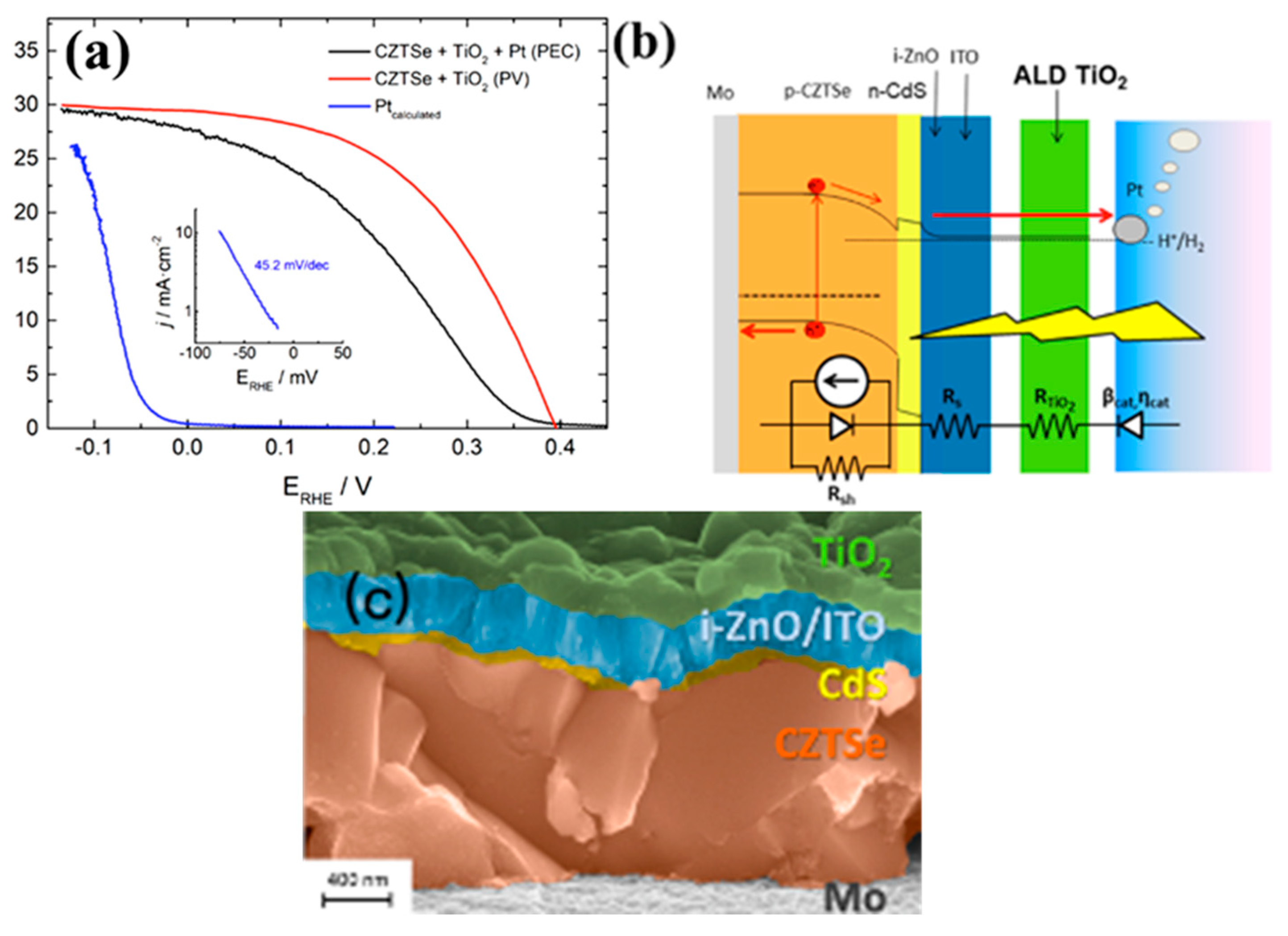
Recent important studies that employs CZTS photocathodes have been summarized in Table 2. In 2010, Yokoyama et al. first demonstrated the application of CZTS as a photocathode. In their work, a series of surface modification works was done to improve the performance of CZTS photocathode. Firstly, in order to increase the charge separation, CdS and TiO2 were deposited on top of CZTS thin-films for surface modification to accelerate charge transfer [89]. N-type CdS can form heterojunction with CZTS, and TiO2 can protect the lower layer from corrosion in acid/alkaline solution. Secondly, in order to promote the H2 evolution reaction, Platinum (Pt) was deposited as a catalyst for the CZTS photocathode. A type-II band structure was formed in the CZTS/CdS/TiO2/Pt photoathode, so the photogenerated electrons facilely transferred from the CZTS to the CdS, and then, through TiO2, migrated into the Pt counter electrode where they were consumed to successfully generate H2 gases. After optimization of the PEC system in electrolyte of different pH values, CZTS photocathode shows the best H2 production to solar energy efficiency of around 1.2% and the highest photocurrent density of around 9 mA/cm2. Yang et al. improved the photocurrent of the device with a similar structure to 13 mA/cm2 through improving the quality of the CZTS layer [90]. In their work, the preparation procedure of the precursor solution containing the metal salts and thiourea was carefully controlled through the addition sequence of each chemical with the characterization of the Liquid Raman Spectra. Ros et al. further improved the solar energy to H2 generation efficiency to 7% by optimizing the thickness of the atomic layer deposited (ALD) TiO2 protecting layer and proceeded the test under highly acidic conditions (PH < 1) [91]. The ALD deposited TiO2 layer plays the role of both an intermediate for electron transfer and a protection layer for the photocathode. A schematic of the system is given in Figure 10b. As shown in the J-V curve in Figure 10a, the Pt catalyst accelerates the H2 reduction kinetics and increases the photocurrent at the photocathode. Due to the toxicity of Cd and the instability problem of CdS, Jiang et al. employed a novel In2S3/CdS double layer on top of the CZTS film [92]. Combined with a Pt catalyst, the designed photocathode showed a significant improvement of stability during photoirradiation for PEC water splitting. The CZTS-based photocathode with novel surface modification achieved a half-cell solar-to-hydrogen efficiency (HC-STH) of 1.63%. The authors further demonstrated a bias-free PEC water splitting system by combining the above CZTS cathodes with a BiVO4 counter photocathode. This was the first published bias free system based on a CZTS photocathode; the full cell power conversion efficiency (PCE) in the designed system was estimated to be 0.28%.
Adjusting the bandgap and CB/VB position is another efficient way to improve the PEC performance of the CZTS photocathode. As we have discussed previously, in the solar cell part, cation doping in CZTS could lead to changes in the bandgap, grain sizes, carrier concentration and defect concentration of CZTS. For example, Cd doping of Zn led to an increased grain size and suppressed formation of the ZnS secondary phase, which resulted in an improved solar cell efficiency. Tay et al. designed a photocathode based on a solution-processed Cu2Cd0.4Zn0.6SnS4 (CCZTS) photoabsorber [93]. After being coated with CdS/TiMo/Pt, the Cu2Cd0.4Zn0.6SnS4 photocathode yielded a photocurrent of 17 mA/cm2 at 0 Vvs RHE, which is more than three times higher than pristine Cu2ZnSnS4. Hall measurement results revealed that CZTS have reduced carrier concentration and much higher carrier mobility after Cd doping, which could be caused by the reduction of CuZn anti-sites. The increased carrier mobility and lower carrier concentration leads to a wider space charge region and results in better charge collection. To further elucidate the reason for the lower onset potential and higher photocurrent for the CCZTS photocathode, an energy diagram based on X-ray photoelectron spectroscopy (XPS) and ultraviolet photoelectron spectroscopy (UPS) was studied. Because the Cd2+ ion is larger than Zn2+, substitution of Zn by Cd induces strain in the kesterite lattice of CZTS, which leads to a ‘spike-like’ conduction band offset at the CCZTS/CdS interface. The formation of a ‘spike-like’ interface plays a key role in reducing interface recombination.
A nanostructured CZTS photocathode has also been studied to enlarge the surface area of the Schottky junction that forms at the solid–electrolyte interface and so increase the separation of photo-generated carriers. In addition, the stronger light absorption and continuous shorter transport distance of photogenerated electrons in a nanostructured thin-film can also contribute to a higher photoelectrode performance than a dense sample. Wen et al. prepared porous nanocrystalline CZTS films by a facile metal organic decomposition (MOD) method through varying the amount of thiourea added in the precursor solution [94]. Compared with dense CZTS electrodes of similar crystallinity, composition and thickness, the porous CZTS photocathode yields much higher (three times) photocurrent. Results from capacitive currents under different scan rates shows that the porous CZTS film has a surface electrochemical area about four times larger than the dense film, which leads to a shorter transport distance of minority carriers and enhanced collected photocurrent in the porous structured CZTS. Instead of producing nanostructure in CZTS, Choi et al. applied CZTS onto a three-dimensional (3D) Cu2ZnSnS4 (CZTS)/CdS/ZnO@steel composite photoanode [95]. The 3D structural photoanode was fabricated by solution method on FTO/steel mesh. A ZnO nanorod was grown by the hydrothermal method onto substrate, followed by CdS deposition using successive ionic layer adsorption reaction (SILAR) and then the spin coating of a CZTS layer using the wet chemical method. A coating of CZTS in this work can act as an efficient light sensitizer to enhance the visible absorption of the composite photoelectrode. A cascade type-II band alignment in the estimated energy diagram of the ZnO/CdS/CZTS system enables efficient charge separation and efficient electron transport across the interfaces of ZnO/CdS and CdS/CZTS. The combination effect of the efficient visible light absorption of CZTS, the cascade bandgaps diagram of the CZTS/CdS/ZnO nanorods and effective light absorption through the 3D structure together lead to a high photocurrent density of 12.5 mA/cm2 at the 0.0 Vvs saturated calomel electrode (SCE).
6. Other Applications of CZTS
Thus far, we have summarized the mainstream application of CZTS in thin-film solar cells as well as two other promising applications as a charge-selective material and a photocathode in photoelectrochemical water splitting. However, there are other interesting applications where CZTS has been employed. In this section, wider potential applications are briefly summarized.
Thermoelectric devices are up-and-coming renewable energy technologies with huge potential that aim to convert heat waste into more useful electrical energy. CZTS can potentially be a thermoelectric material because of its highly distorted crystal structure, which results low thermal conductivity while having tuneable electrical properties. An important study showing that CZTS can exhibit good thermoelectrical properties was performed by Shi et al. in 2009 [96]. In that study, low thermal conductivity of CZTSe was combined with high electrical conductivity achieved by introducing indium impurities into a Cu2ZnSnSe4 lattice. An ideal composition was found at Cu2ZnSn0.9In0.1Se4, where the dimensionless figure of merit ZT reaches 0.37 at 700 K. Other studies employed Cu doping to achieve higher ZT values. Chen et al. reached ZT values of 0.7 at 450 °C thorough Cu doping [97]. Studies show that the thermoelectric properties of CZTSe increase with increasing temperatures [98], while stability issues become a problem at temperatures above 550 °C.
CZTS thin-films have been employed as photodetectors in a few studies [99,100,101], thanks to its appropriate optical properties. Singh et al. observed a significant improvement in the response rise time and photocurrent across near infrared to the visible region for Na doped CZTS photodetectors compared to un-doped CZTS [99]. Gour et al. fabricated rice-like nanostructured CZTS through sputtering in order to improve optical absorption, which resulted in a lower response rise time and decay times [100]. In a more recent study, Li et al. established a CZTS/ZnO heterojunction photodetector from vertically aligned ZnO nanorods and CZTS nanoparticles. The resulting photodetector exhibited high responsivity with fast rise and decay times [101].
CZTS can also be employed in a variety of sensors. Previously, CZTS-based liquefied petroleum gas (LPG) sensors with different heterojunction partners, such as polyaniline [102,103] and ZnO [104], have been presented. Studies have shown that the J-V characteristics of CZTS respond to LPG significantly differently than N2, O2, H2 and CO2, allowing detection. With its fast response time and high stability, CZTS could be a contestant to existing technologies in this area. Apart from LPG sensors, a novel biosensor for uric acid detection has been developed by Jain et al. based on uricase/CZTS/ITO/glass electrodes, which showed high sensitivity with a fast response time and a low detection limit towards uric acid [105].
7. Summary and Outlook
Kesterite CZTS, and its variants, has attracted great attention as a new absorber material for thin-film photovoltaic because of its earth-abundant, non-toxic and highly stable nature and the fact that it has similar properties to already commercial thin-film photovoltaic material CIGS. This makes it easier to develop higher performance CZTS-based devices by adapting concepts and know-how from CIGS. Since its introduction, the record device efficiency of CZTS increased steadily until it reached a stagnation point a few years ago. Despite this slowdown, important developments and progress have been made in the past few years in terms of understanding the material properties as well as developing new strategies to reach higher performances. The main problems that limit the efficiency of CZTS solar cells, including the Voc deficit, non-ideal junction interfaces and deep-level intrinsic defects in the bulk CZTS, are yet to be addressed and solved. One proposed method to overcome these challenges is alkali metal doping. Specifically, Li, Na and K doping have been proven by many researchers to be highly beneficial for device performance. Cation substitution and alloying also promise interesting options. As a fairly complicated material, the components of CZTS can be substituted by keeping an I2-II-IV-VI4 structure, which allows the fine tuning of optoelectrical properties. Current promising alternatives are Ag substitution for Cu, Cd substitution for Zn and Ge substitution for Sn. However, there are also many more that could be explored. On the other hand, the advantages and interesting properties of CZTS also make it viable for various other applications. One of these potential applications is the use of CZTS as a hole transport layer in perovskite solar cells. A handful of studies have already proven it as a concept, and in the near future, by finely tuning the material properties, high performance perovskite devices could be produced. Another alternative application is using CZTS as a photocathode in photoelectrochemical water splitting for green hydrogen production. CZTS could have a bright future in this area, specifically as a result of its highly tuneable valence and conduction band edges through cation/anion substitution. CZTS can also be used as a thermoelectric material. Its highly disorganized crystal lattice causes low heat conductivity while its electronic properties can be improved by extrinsic doping. Lastly, some studies have shown that CZTS can also be used in photodetectors and gas sensors.
Author Contributions
Writing—original draft preparation, review and editing A.S.N. and M.W.; Writing—review and editing K.L.C.; Supervision K.L.C. All authors have read and agreed to the published version of the manuscript
Funding
The support of the Innovate UK-High Prospect project (No. 102470) and the EU-SCALENANO Project (No. NMP4-LA-2011-284486) are gratefully acknowledged. A.S.N. would also like to thank the Republic of Turkey Ministry of National Education for sponsoring his PhD studies under the YLSY sponsorship scheme.
Conflicts of Interest
The authors declare no conflict of interest.
References
- International Energy Agency. World Energy Balances 2018: Overview; IEA: Paris, France, 2018; ISBN 978-92-64-30156-6.
- International Renewable Energy Agency. Global Energy Transformation: A Roadmap to 2050, 2019th ed.; IRENA: Abu Dhabi, UAE, 2019; ISBN 978-92-9260-121-8.
- Richter, A.; Hermle, M.; Glunz, S.W. Reassessment of the Limiting Efficiency for Crystalline Silicon Solar Cells. IEEE J. Photovolt. 2013, 3, 1184–1191. [Google Scholar] [CrossRef]
- Yoshikawa, K.; Hayato, K.; Wataru, Y.; Toru, I.; Katsunori, K.; Kunihiro, N.; Toshihiko, U.; Daisuke, A.; Masanori, K.; Hisashi, U.; et al. Silicon heterojunction solar cell with interdigitated back contacts for a photoconversion efficiency over 26%. Nat. Energy 2017, 2, 17032. [Google Scholar] [CrossRef]
- Green, M.A.; Dunlop, E.D.; Hohl-Ebinger, J.; Yoshita, M.; Kopidakis, N.; Ho-Baillie, A.W.Y. Solar cell efficiency tables (Version 55). Prog. Photovolt. Res. Appl. 2020, 28, 3–15. [Google Scholar] [CrossRef]
- Fraunhofer Institute for Solar Energy Systems. Photovoltaics Report 2018; Fraunhofer ISE: Freiberg, Germany, 2018. [Google Scholar]
- Yang, W.S.; Noh, J.H.; Jeon, N.J.; Kim, Y.C.; Ryu, S.; Seo, J.; Seok, S.I. High-performance photovoltaic perovskite layers fabricated through intramolecular exchange. Science 2015, 348, 1234–1237. [Google Scholar] [CrossRef] [PubMed]
- Kojima, A.; Teshima, K.; Shirai, Y.; Miyasaka, T. Organometal Halide Perovskites as Visible-Light Sensitizers for Photovoltaic Cells. J. Am. Chem. Soc. 2009, 131, 6050–6051. [Google Scholar] [CrossRef] [PubMed]
- Wang, W.; Winkler, M.T.; Gunawan, O.; Gokmen, T.; Todorov, T.K.; Zhu, Y.; Mitzi, D.B. Device Characteristics of CZTSSe Thin-Film Solar Cells with 12.6% Efficiency. Adv. Energy Mater. 2014, 4, 1301465. [Google Scholar] [CrossRef]
- Walsh, A.; Chen, S.; Wei, S.-H.; Gong, X.-G. Kesterite Thin-Film Solar Cells: Advances in Materials Modelling of Cu2ZnSnS4. Adv. Energy Mater. 2012, 2, 400–409. [Google Scholar] [CrossRef]
- Chang, J.; Waclawik, E.R. Colloidal semiconductor nanocrystals: Controlled synthesis and surface chemistry in organic media. RSC Adv. 2014, 4, 23505–23527. [Google Scholar] [CrossRef] [Green Version]
- Goodman, C.H.L. The prediction of semiconducting properties in inorganic compounds. J. Phys. Chem. Solids 1958, 6, 305–314. [Google Scholar] [CrossRef]
- Pamplin, B.R. A systematic method of deriving new semiconducting compounds by structural analogy. J. Phys. Chem. Solids 1964, 25, 675–684. [Google Scholar] [CrossRef]
- Romanyuk, Y.E.; Haass, S.G.; Giraldo, S.; Placidi, M.; Tiwari, D.; Fermin, D.J.; Hao, X.; Xin, H.; Schnabel, T.; Kauk-Kuusik, M.; et al. Doping and alloying of kesterites. J. Phys. Energy 2019, 1, 044004. [Google Scholar] [CrossRef] [Green Version]
- Schorr, S. The crystal structure of kesterite type compounds: A neutron and X-ray diffraction study. Sol. Energy Mater. Sol. Cells 2011, 95, 1482–1488. [Google Scholar] [CrossRef]
- Lafond, A.; Choubrac, L.; Guillot-Deudon, C.; Deniard, P.; Jobic, S. Crystal Structures of Photovoltaic Chalcogenides, an Intricate Puzzle to Solve: The Cases of CIGSe and CZTS Materials. Zeitschrift Für Anorganische und Allgemeine Chemie 2012, 638, 2571–2577. [Google Scholar] [CrossRef]
- Liu, X.; Feng, Y.; Cui, H.; Liu, F.; Hao, X.; Conibeer, G.; Mitzi, D.B.; Green, M. The current status and future prospects of kesterite solar cells: A brief review. Prog. Photovolt. Res. Appl. 2016, 24, 879–898. [Google Scholar] [CrossRef]
- Chen, S.; Gong, X.G.; Wei, S.-H. Band-structure anomalies of the chalcopyrite semiconductors CuGaX2 versus AgGaX2 (X = S and Se) and their alloys. Phys. Rev. B 2007, 75, 205209. [Google Scholar] [CrossRef] [Green Version]
- Chen, S.; Gong, X.G.; Walsh, A.; Wei, S.-H. Electronic structure and stability of quaternary chalcogenide semiconductors derived from cation cross-substitution of II-VI and I-III-VI2 compounds. Phys. Rev. B 2009, 79, 165211. [Google Scholar] [CrossRef]
- Chen, S.; Walsh, A.; Yang, J.-H.; Gong, X.G.; Sun, L.; Yang, P.-X.; Chu, J.-H.; Wei, S.-H. Compositional dependence of structural and electronic properties of Cu2ZnSn(S,Se)4 alloys for thin film solar cells. Phys. Rev. B 2011, 83, 125201. [Google Scholar] [CrossRef] [Green Version]
- Chen, S.; Yang, J.-H.; Gong, X.G.; Walsh, A.; Wei, S.-H. Intrinsic point defects and complexes in the quaternary kesterite semiconductor Cu2ZnSnS4. Phys. Rev. B 2010, 81, 245204. [Google Scholar] [CrossRef] [Green Version]
- Chen, S.; Walsh, A.; Gong, X.-G.; Wei, S.-H. Classification of Lattice Defects in the Kesterite Cu2ZnSnS4 and Cu2ZnSnSe4 Earth-Abundant Solar Cell Absorbers. Adv. Mater. 2013, 25, 1522–1539. [Google Scholar] [CrossRef]
- Kumar, M.; Dubey, A.; Adhikari, N.; Venkatesan, S.; Qiao, Q. Strategic review of secondary phases, defects and defect-complexes in kesterite CZTS–Se solar cells. Energy Environ. Sci. 2015, 8, 3134–3159. [Google Scholar] [CrossRef]
- Huang, T.J.; Yin, X.; Qi, G.; Gong, H. CZTS-based materials and interfaces and their effects on the performance of thin film solar cells. Phys. Status Solidi RRL Rapid Res. Lett. 2014, 8, 735–762. [Google Scholar] [CrossRef]
- Grossberg, M.; Krustok, J.; Raudoja, J.; Timmo, K.; Altosaar, M.; Raadik, T. Photoluminescence and Raman study of Cu2ZnSn(SexS1−x)4 monograins for photovoltaic applications. Thin Solid Film. 2011, 519, 7403–7406. [Google Scholar] [CrossRef]
- Gokmen, T.; Gunawan, O.; Todorov, T.K.; Mitzi, D.B. Band tailing and efficiency limitation in kesterite solar cells. Appl. Phys. Lett. 2013, 103, 103506. [Google Scholar] [CrossRef]
- Chen, S.; Gong, X.G.; Walsh, A.; Wei, S.-H. Defect physics of the kesterite thin-film solar cell absorber Cu2ZnSnS4. Appl. Phys. Lett. 2010, 96, 21902. [Google Scholar] [CrossRef]
- Malerba, C.; Biccari, F.; Azanza Ricardo, C.L.; Valentini, M.; Chierchia, R.; Müller, M.; Santoni, A.; Esposito, E.; Mangiapane, P.; Scardi, P.; et al. CZTS stoichiometry effects on the band gap energy. J. Alloys Compd. 2014, 582, 528–534. [Google Scholar] [CrossRef]
- Caballero, R.; Garcia-Llamas, E.; Merino, J.M.; León, M.; Babichuk, I.; Dzhagan, V.; Strelchuk, V.; Valakh, M. Non-stoichiometry effect and disorder in Cu2ZnSnS4 thin films obtained by flash evaporation: Raman scattering investigation. Acta Mater. 2014, 65, 412–417. [Google Scholar] [CrossRef] [Green Version]
- Yu, K.; Carter, E.A. Determining and Controlling the Stoichiometry of Cu2ZnSnS4 Photovoltaics: The Physics and Its Implications. Chem. Mater. 2016, 28, 4415–4420. [Google Scholar] [CrossRef]
- Paris, M.; Choubrac, L.; Lafond, A.; Guillot-Deudon, C.; Jobic, S. Solid-State NMR and Raman Spectroscopy to Address the Local Structure of Defects and the Tricky Issue of the Cu/Zn Disorder in Cu-Poor, Zn-Rich CZTS Materials. Inorg. Chem. 2014, 53, 8646–8653. [Google Scholar] [CrossRef]
- Katagiri, H.; Sasaguchi, N.; Hando, S.; Hoshino, S.; Ohashi, J.; Yokota, T. Preparation and evaluation of Cu2ZnSnS4 thin films by sulfurization of E B evaporated precursors. Sol. Energy Mater. Sol. Cells 1997, 49, 407–414. [Google Scholar] [CrossRef]
- Todorov, T.K.; Reuter, K.B.; Mitzi, D.B. High-Efficiency Solar Cell with Earth-Abundant Liquid-Processed Absorber. Adv. Mater. 2010, 22, E156–E159. [Google Scholar] [CrossRef]
- Barkhouse, D.; Aaron, R.; Gunawan, O.; Gokmen, T.; Todorov, T.K.; Mitzi, D.B. Device characteristics of a 10.1% hydrazine-processed Cu2ZnSn(Se,S)4 solar cell. Prog. Photovolt. Res. Appl. 2012, 20, 6–11. [Google Scholar] [CrossRef]
- Repins, I.; Beall, C.; Vora, N.; DeHart, C.; Kuciauskas, D.; Dippo, P.; To, B.; Mann, J.; Hsu, W.-C.; Goodrich, A.; et al. Co-evaporated Cu2ZnSnSe4 films and devices. Sol. Energy Mater. Sol. Cells 2012, 101, 154–159. [Google Scholar] [CrossRef]
- Todorov, T.K.; Gunawan, O.; Gokmen, T.; Mitzi, D.B. Solution-processed Cu(In,Ga)(S,Se)2 absorber yielding a 15.2% efficient solar cell. Prog. Photovolt. Res. Appl. 2013, 21, 82–87. [Google Scholar] [CrossRef]
- Mitzi, D.B. Solution Processing of Chalcogenide Semiconductors via Dimensional Reduction. Adv. Mater. 2009, 21, 3141–3158. [Google Scholar] [CrossRef]
- Kim, J.; Hiroi, H.; Todorov, T.K.; Gunawan, O.; Kuwahara, M.; Gokmen, T.; Nair, D.; Hopstaken, M.; Shin, B.; Lee, Y.S.; et al. High Efficiency Cu2ZnSn(S,Se)4 Solar Cells by Applying a Double In2S3/CdS Emitter. Adv. Mater. 2014, 26, 7427–7431. [Google Scholar] [CrossRef]
- Todorov, T.K.; Tang, J.; Bag, S.; Gunawan, O.; Gokmen, T.; Zhu, Y.; Mitzi, D.B. Beyond 11% Efficiency: Characteristics of State-of-the-Art Cu2ZnSn(S,Se)4 Solar Cells. Adv. Energy Mater. 2013, 3, 34–38. [Google Scholar] [CrossRef]
- Todorov, T.; Sugimoto, H.; Gunawan, O.; Gokmen, T.; Mitzi, D.B. High-Efficiency Devices With Pure Solution-Processed Cu2ZnSn(S,Se)4 Absorbers. IEEE J. Photovolt. 2014, 4, 483–485. [Google Scholar] [CrossRef]
- Su, Z.; Sun, K.; Han, Z.; Cui, H.; Liu, F.; Lai, Y.; Li, J.; Hao, X.; Liu, Y.; Green, M.A. Fabrication of Cu2ZnSnS4 solar cells with 5.1% efficiency via thermal decomposition and reaction using a non-toxic sol–gel route. J. Mater. Chem. A 2014, 2, 500–509. [Google Scholar] [CrossRef]
- Liu, F.; Zeng, F.; Song, N.; Jiang, L.; Han, Z.; Su, Z.; Yan, C.; Wen, X.; Hao, X.; Liu, Y. Kesterite Cu2ZnSn(S,Se)4 Solar Cells with beyond 8% Efficiency by a Sol–Gel and Selenization Process. ACS Appl. Mater. Interfaces 2015, 7, 14376–14383. [Google Scholar] [CrossRef]
- Ki, W.; Hillhouse, H.W. Earth-Abundant Element Photovoltaics Directly from Soluble Precursors with High Yield Using a Non-Toxic Solvent. Adv. Energy Mater. 2011, 1, 732–735. [Google Scholar] [CrossRef]
- Xin, H.; Katahara, J.K.; Braly, I.L.; Hillhouse, H.W. 8% Efficient Cu2ZnSn(S,Se)4 Solar Cells from Redox Equilibrated Simple Precursors in DMSO. Adv. Energy Mater. 2014, 4, 1301823. [Google Scholar] [CrossRef]
- Xin, H.; Vorpahl, S.M.; Collord, A.D.; Braly, I.L.; Uhl, A.R.; Krueger, B.W.; Ginger, D.S.; Hillhouse, H.W. Lithium-doping inverts the nanoscale electric field at the grain boundaries in Cu2ZnSn(S,Se)4 and increases photovoltaic efficiency. Phys. Chem. Chem. Phys. 2015, 17, 23859–23866. [Google Scholar] [CrossRef] [PubMed]
- Haass, S.G.; Diethelm, M.; Werner, M.; Bissig, B.; Romanyuk, Y.E.; Tiwari, A.N. 11.2% Efficient Solution Processed Kesterite Solar Cell with a Low Voltage Deficit. Adv. Energy Mater. 2015, 5, 1500712. [Google Scholar] [CrossRef]
- Schnabel, T.; Abzieher, T.; Friedlmeier, T.M.; Ahlswede, E. Solution-Based Preparation of Cu2ZnSn(S,Se)4 for Solar Cells—Comparison of SnSe2 and Elemental Se as Chalcogen Source. IEEE J. Photovolt. 2015, 5, 670–675. [Google Scholar] [CrossRef]
- Calvet, I.; Barrachina, E.; Martí, R.; Fraga, D.; Stoyanova Lyubenova, T.; Carda, J.B. Development of photovoltaic ceramic tile based on CZTSSe absorber. Mater. Lett. 2015, 161, 636–639. [Google Scholar] [CrossRef]
- Giraldo, S.; Jehl, Z.; Placidi, M.; Izquierdo-Roca, V.; Pérez-Rodríguez, A.; Saucedo, E. Progress and Perspectives of Thin Film Kesterite Photovoltaic Technology: A Critical Review. Adv. Mater. 2019, 31, 1806692. [Google Scholar] [CrossRef] [Green Version]
- Granath, K.; Bodegrd, M.; Stolt, L. The effect of NaF on Cu(In,Ga)Se2 thin film solar cells. Sol. Energy Mater. Sol. Cells 2000, 60, 279–293. [Google Scholar] [CrossRef]
- Gershon, T.; Shin, B.; Bojarczuk, N.; Hopstaken, M.; Mitzi, D.B.; Guha, S. The Role of Sodium as a Surfactant and Suppressor of Non-Radiative Recombination at Internal Surfaces in Cu2ZnSnS4. Adv. Energy Mater. 2015, 5, 1400849. [Google Scholar] [CrossRef]
- Sutter-Fella, C.M.; Stckelberger, J.A.; Hagendorfer, H.; La Mattina, F.; Kranz, L.; Nishiwaki, S.; Uhl, A.R.; Romanyuk, Y.E.; Tiwari, A.N. Sodium Assisted Sintering of Chalcogenides and Its Application to Solution Processed Cu2ZnSn(S,Se)4 Thin Film Solar Cells. Chem. Mater. 2014, 26, 1420–1425. [Google Scholar] [CrossRef]
- Zhou, H.; Song, T.-B.; Hsu, W.-C.; Luo, S.; Ye, S.; Duan, H.-S.; Hsu, C.-J.; Yang, W.; Yang, Y. Rational Defect Passivation of Cu2ZnSn(S,Se)4 Photovoltaics with Solution-Processed Cu2ZnSnS4:Na Nanocrystals. J. Am. Chem. Soc. 2013, 135, 15998–16001. [Google Scholar] [CrossRef]
- Gershon, T.; Lee, Y.S.; Mankad, R.; Gunawan, O.; Gokmen, T.; Bishop, D.; McCandless, B.; Guha, S. The impact of sodium on the sub-bandgap states in CZTSe and CZTS. Appl. Phys. Lett. 2015, 106, 123905. [Google Scholar] [CrossRef]
- Cabas-Vidani, A.; Haass, S.G.; Andres, C.; Caballero, R.; Figi, R.; Schreiner, C.; Márquez, J.A.; Hages, C.; Unold, T.; Bleiner, D.; et al. High-Efficiency (LixCu1−x)2ZnSn(S,Se)4 Kesterite Solar Cells with Lithium Alloying. Adv. Energy Mater. 2018, 8, 1801191. [Google Scholar] [CrossRef]
- Altamura, G.; Wang, M.; Choy, K.-L. Influence of alkali metals (Na, Li, Rb) on the performance of electrostatic spray-assisted vapor deposited Cu2ZnSn(S,Se)4 solar cells. Sci. Rep. 2016, 6, 22109. [Google Scholar] [CrossRef] [PubMed]
- Tong, Z.; Yan, C.; Su, Z.; Zeng, F.; Yang, J.; Li, Y.; Jiang, L.; Lai, Y.; Liu, F. Effects of potassium doping on solution processed kesterite Cu2ZnSnS4 thin film solar cells. Appl. Phys. Lett. 2014, 105, 223903. [Google Scholar] [CrossRef]
- Wang, C.; Chen, S.; Yang, J.-H.; Lang, L.; Xiang, H.-J.; Gong, X.-G.; Walsh, A.; Wei, S.-H. Design of I2–II–IV–VI4 Semiconductors through Element Substitution: The Thermodynamic Stability Limit and Chemical Trend. Chem. Mater. 2014, 26, 3411–3417. [Google Scholar] [CrossRef] [Green Version]
- Zhu, T.; Huhn, W.P.; Wessler, G.C.; Shin, D.; Saparov, B.; Mitzi, D.B.; Blum, V. I2–II–IV–VI4 (I = Cu, Ag; II = Sr, Ba; IV = Ge, Sn; VI = S, Se): Chalcogenides for Thin-Film Photovoltaics. Chem. Mater. 2017, 29, 7868–7879. [Google Scholar] [CrossRef]
- Yuan, Z.-K.; Chen, S.; Xiang, H.; Gong, X.-G.; Walsh, A.; Park, J.-S.; Repins, I.; Wei, S.-H. Engineering Solar Cell Absorbers by Exploring the Band Alignment and Defect Disparity: The Case of Cu- and Ag-Based Kesterite Compounds. Adv. Funct. Mater. 2015, 25, 6733–6743. [Google Scholar] [CrossRef]
- Chagarov, E.; Sardashti, K.; Kummel, A.C.; Lee, Y.S.; Haight, R.; Gershon, T.S. Ag2ZnSn(S,Se)4: A highly promising absorber for thin film photovoltaics. J. Chem. Phys. 2016, 144, 104704. [Google Scholar] [CrossRef] [PubMed]
- Gershon, T.; Sardashti, K.; Gunawan, O.; Mankad, R.; Singh, S.; Lee, Y.S.; Ott, J.A.; Kummel, A.; Haight, R. Photovoltaic Device with over 5% Efficiency Based on an n-Type Ag2ZnSnSe4 Absorber. Adv. Energy Mater. 2016, 6, 1601182. [Google Scholar] [CrossRef]
- Guchhait, A.; Su, Z.; Tay, Y.F.; Shukla, S.; Li, W.; Leow, S.W.; Tan, J.M.R.; Lie, S.; Gunawan, O.; Wong, L.H. Enhancement of Open-Circuit Voltage of Solution-Processed Cu2ZnSnS4 Solar Cells with 7.2% Efficiency by Incorporation of Silver. ACS Energy Lett. 2016, 1, 1256–1261. [Google Scholar] [CrossRef] [Green Version]
- Guo, H.; Ma, C.; Zhang, K.; Jia, X.; Li, Y.; Yuan, N.; Ding, J. The fabrication of Cd-free Cu2ZnSnS4-Ag2ZnSnS4 heterojunction photovoltaic devices. Sol. Energy Mater. Sol. Cells 2018, 178, 146–153. [Google Scholar] [CrossRef]
- Ma, C.; Guo, H.; Zhang, K.; Li, Y.; Yuan, N.; Ding, J. The preparation of Ag2ZnSnS4 homojunction solar cells. Mater. Lett. 2017, 207, 209–212. [Google Scholar] [CrossRef]
- Kumar, J.; Ingole, S. Structural and optical properties of (AgxCu1-x)2ZnSnS4 thin films synthesised via solution route. J. Alloys Compd. 2017, 727, 1089–1094. [Google Scholar] [CrossRef]
- Gershon, T.; Sardashti, K.; Lee, Y.S.; Gunawan, O.; Singh, S.; Bishop, D.; Kummel, A.C.; Haight, R. Compositional effects in Ag2ZnSnSe4 thin films and photovoltaic devices. Acta Mater. 2017, 126, 383–388. [Google Scholar] [CrossRef] [Green Version]
- Xiao, Z.-Y.; Li, Y.-F.; Yao, B.; Deng, R.; Ding, Z.-H.; Wu, T.; Yang, G.; Li, C.-R.; Dong, Z.-Y.; Liu, L.; et al. Bandgap engineering of Cu2CdxZn1−xSnS4 alloy for photovoltaic applications: A complementary experimental and first-principles study. J. Appl. Phys. 2013, 114, 183506. [Google Scholar] [CrossRef] [Green Version]
- Su, Z.; Tan, J.M.R.; Li, X.; Zeng, X.; Batabyal, S.K.; Wong, L.H. Cation Substitution of Solution-Processed Cu2ZnSnS4 Thin Film Solar Cell with over 9% Efficiency. Adv. Energy Mater. 2015, 5, 1500682. [Google Scholar] [CrossRef]
- Chatterjee, S.; Pal, A.J. A solution approach to p-type Cu2FeSnS4 thin-films and pn-junction solar cells: Role of electron selective materials on their performance. Sol. Energy Mater. Sol. Cells 2017, 160, 233–240. [Google Scholar] [CrossRef]
- Chen, L.; Deng, H.; Cui, J.; Tao, J.; Zhou, W.; Cao, H.; Sun, L.; Yang, P.; Chu, J. Composition dependence of the structure and optical properties of Cu2MnxZn1−xSnS4 thin films. J. Alloys Compd. 2015, 627, 388–392. [Google Scholar] [CrossRef]
- Hages, C.J.; Levcenco, S.; Miskin, C.K.; Alsmeier, J.H.; Abou-Ras, D.; Wilks, R.G.; Bär, M.; Unold, T.; Agrawal, R. Improved performance of Ge-alloyed CZTGeSSe thin-film solar cells through control of elemental losses. Prog. Photovolt. Res. Appl. 2015, 23, 376–384. [Google Scholar] [CrossRef]
- Collord, A.D.; Hillhouse, H.W. Germanium Alloyed Kesterite Solar Cells with Low Voltage Deficits. Chem. Mater. 2016, 28, 2067–2073. [Google Scholar] [CrossRef]
- Kim, S.; Kim, K.M.; Tampo, H.; Shibata, H.; Niki, S. Improvement of voltage deficit of Ge-incorporated kesterite solar cell with 12.3% conversion efficiency. Appl. Phys. Express 2016, 9, 102301. [Google Scholar] [CrossRef]
- Choubrac, L.; Brammertz, G.; Barreau, N.; Arzel, L.; Harel, S.; Meuris, M.; Vermang, B. 7.6% CZGSe Solar Cells Thanks to Optimized CdS Chemical Bath Deposition. Phys. Status Solidi A 2018, 215, 1800043. [Google Scholar] [CrossRef] [Green Version]
- Wu, Q.; Xue, C.; Li, Y.; Zhou, P.; Liu, W.; Zhu, J.; Dai, S.; Zhu, C.; Yang, S. Kesterite Cu2ZnSnS4 as a Low-Cost Inorganic Hole-Transporting Material for High-Efficiency Perovskite Solar Cells. ACS Appl. Mater. Interfaces 2015, 7, 28466–28473. [Google Scholar] [CrossRef] [PubMed]
- Khanzada, L.S.; Levchuk, I.; Hou, Y.; Azimi, H.; Osvet, A.; Ahmad, R.; Brandl, M.; Herre, P.; Distaso, M.; Hock, R.; et al. Effective Ligand Engineering of the Cu2ZnSnS4 Nanocrystal Surface for Increasing Hole Transport Efficiency in Perovskite Solar Cells. Adv. Funct. Mater. 2016, 26, 8300–8306. [Google Scholar] [CrossRef]
- Yuan, M.; Zhang, X.; Kong, J.; Zhou, W.; Zhou, Z.; Tian, Q.; Meng, Y.; Wu, S.; Kou, D. Controlling the Band Gap to Improve Open-Circuit Voltage in Metal Chalcogenide based Perovskite Solar Cells. Electrochim. Acta 2016, 215, 374–379. [Google Scholar] [CrossRef]
- Nan, H.; Han, J.; Yin, X.; Zhou, Y.; Yao, Z.; Li, X.; Lin, H. Reduced Graphene Oxide/CZTSxSe1-x Composites as a Novel Hole-Transport Functional Layer in Perovskite Solar Cells. ChemElectroChem 2019, 6, 1500–1507. [Google Scholar] [CrossRef]
- Patel, S.B.; Patel, A.H.; Gohel, J.V. A novel and cost effective CZTS hole transport material applied in perovskite solar cells. CrystEngComm 2018, 20, 7677–7687. [Google Scholar] [CrossRef]
- Ashebir, G.Y.; Dong, C.; Wan, Z.; Qi, J.; Chen, J.; Zhao, Q.; Chen, W.; Wang, M. Solution-processed Cu2ZnSnS4 nanoparticle film as efficient hole transporting layer for stable perovskite solar cells. J. Phys. Chem. Solids 2019, 129, 204–208. [Google Scholar] [CrossRef]
- Zhou, Z.-J.; Deng, Y.-Q.; Zhang, P.-P.; Kou, D.-X.; Zhou, W.-H.; Meng, Y.-N.; Yuan, S.-J.; Wu, S.-X. Cu2ZnSnS4 Quantum Dots as Hole Transport Material for Enhanced Charge Extraction and Stability in All-Inorganic CsPbBr3 Perovskite Solar Cells. Sol. RRL 2019, 3, 1800354. [Google Scholar] [CrossRef]
- Khattak, Y.H.; Baig, F.; Toura, H.; Beg, S.; Soucase, B.M. CZTSe Kesterite as an Alternative Hole Transport Layer for MASnI3 Perovskite Solar Cells. J. Electron. Mater. 2019, 48, 5723–5733. [Google Scholar] [CrossRef]
- Lingyan, L.; Linqin, J.; Ping, L.; Xiaoyan, L.; Yu, Q. Numerical modeling of inverted perovskite solar cell based on CZTSSe hole transport layer for efficiency improvement. J. Photonics Energy 2019, 9, 1–11. [Google Scholar] [CrossRef]
- Sanad, M.M.S.; Elseman, A.M.; Elsenety, M.M.; Rashad, M.M.; Elsayed, B.A. Facile synthesis of sulfide-based chalcogenide as hole-transporting materials for cost-effective efficient perovskite solar cells. J. Mater. Sci. Mater. Electron. 2019, 30, 6868–6875. [Google Scholar] [CrossRef]
- Shadrokh, Z.; Sousani, S.; Gholipour, S.; Abdi, Y. Enhanced stability and performance of poly(4-vinylpyridine) modified perovskite solar cell with quaternary semiconductor Cu2MSnS4 (M = Co2+, Ni2+, Zn2+) as hole transport materials. Sol. Energy Mater. Sol. Cells 2020, 211, 110538. [Google Scholar] [CrossRef]
- Cao, Y.; Wu, H.; Li, W.; Zhao, Z.; Xiao, Z.; Zi, W.; Cheng, N.; Liu, J.; Tu, Y. Cu2ZnSnS4 as an efficient hole transporting material for low temperature paintable carbon electrode based perovskite solar cells. Org. Electron. 2020, 76, 105455. [Google Scholar] [CrossRef]
- Patel, S.; Gohel, J. Recent Developments in Cu2ZnSnS4 (CZTS) Preparation, Optimization and its Application in Solar Cell Development and Photocatalytic Applications. In Photocatalytic Nanomaterials for Environmental Applications; Materials Research Forum LLC: Millersville, PA, USA, 2018; pp. 370–404. [Google Scholar] [CrossRef]
- Yokoyama, D.; Minegishi, T.; Jimbo, K.; Hisatomi, T.; Ma, G.; Katayama, M.; Kubota, J.; Katagiri, H.; Domen, K. H2 Evolution from Water on Modified Cu2ZnSnS4 Photoelectrode under Solar Light. Appl. Phys. Express 2010, 3, 101202. [Google Scholar] [CrossRef]
- Yang, W.; Oh, Y.; Kim, J.; Jeong, M.J.; Park, J.H.; Moon, J. Molecular Chemistry-Controlled Hybrid Ink-Derived Efficient Cu2ZnSnS4 Photocathodes for Photoelectrochemical Water Splitting. ACS Energy Lett. 2016, 1, 1127–1136. [Google Scholar] [CrossRef]
- Ros, C.; Andreu, T.; Giraldo, S.; Izquierdo-Roca, V.; Saucedo, E.; Morante, J.R. Turning Earth Abundant Kesterite-Based Solar Cells Into Efficient Protected Water-Splitting Photocathodes. ACS Appl. Mater. Interfaces 2018, 10, 13425–13433. [Google Scholar] [CrossRef]
- Jiang, F.; Gunawan; Harada, T.; Kuang, Y.; Minegishi, T.; Domen, K.; Ikeda, S. Pt/In2S3/CdS/Cu2ZnSnS4 Thin Film as an Efficient and Stable Photocathode for Water Reduction under Sunlight Radiation. J. Am. Chem. Soc. 2015, 137, 13691–13697. [Google Scholar] [CrossRef]
- Tay, Y.F.; Kaneko, H.; Chiam, S.Y.; Lie, S.; Zheng, Q.; Wu, B.; Hadke, S.S.; Su, Z.; Bassi, P.S.; Bishop, D.; et al. Solution-Processed Cd-Substituted CZTS Photocathode for Efficient Solar Hydrogen Evolution from Neutral Water. Joule 2018, 2, 537–548. [Google Scholar] [CrossRef] [Green Version]
- Wen, X.; Luo, W.; Zou, Z. Photocurrent improvement in nanocrystalline Cu2ZnSnS4 photocathodes by introducing porous structures. J. Mater. Chem. A 2013, 1, 15479–15485. [Google Scholar] [CrossRef]
- Choi, Y.; Baek, M.; Zhang, Z.; Dao, V.-D.; Choi, H.-S.; Yong, K. A two-storey structured photoanode of a 3D Cu2ZnSnS4/CdS/ZnO@steel composite nanostructure for efficient photoelectrochemical hydrogen generation. Nanoscale 2015, 7, 15291–15299. [Google Scholar] [CrossRef] [PubMed]
- Shi, X.Y.; Huang, F.Q.; Liu, M.L.; Chen, L.D. Thermoelectric properties of tetrahedrally bonded wide-gap stannite compounds Cu2ZnSn1−xInxSe4. Appl. Phys. Lett. 2009, 94, 122103. [Google Scholar] [CrossRef]
- Chen, D.; Zhao, Y.; Chen, Y.; Wang, B.; Wang, Y.; Zhou, J.; Liang, Z. Hot-Injection Synthesis of Cu-Doped Cu2ZnSnSe4 Nanocrystals to Reach Thermoelectric zT of 0.70 at 450 °C. ACS Appl. Mater. Interfaces 2015, 7, 24403–24408. [Google Scholar] [CrossRef] [PubMed]
- Yang, H.; Jauregui, L.A.; Zhang, G.; Chen, Y.P.; Wu, Y. Nontoxic and Abundant Copper Zinc Tin Sulfide Nanocrystals for Potential High-Temperature Thermoelectric Energy Harvesting. Nano Lett. 2012, 12, 540–545. [Google Scholar] [CrossRef] [PubMed] [Green Version]
- Singh, O.P.; Sharma, A.; Gour, K.S.; Husale, S.; Singh, V.N. Fast switching response of Na-doped CZTS photodetector from visible to NIR range. Sol. Energy Mater. Sol. Cells 2016, 157, 28–34. [Google Scholar] [CrossRef]
- Gour, K.S.; Bhattacharyya, B.; Singh, O.P.; Yadav, A.K.; Husale, S.; Singh, V.N. Nanostructured Cu2ZnSnS4 (CZTS) thin film for self-powered broadband photodetection. J. Alloys Compd. 2018, 735, 285–290. [Google Scholar] [CrossRef]
- Li, W.; Xiong, D.; Xie, M.; Luo, C.; Zeng, X.; Gao, Y.; Guo, B.; Yan, C.; Chun, F.; Zhu, Z.; et al. Coaxially enhanced photocarrier transport of a highly oriented Cu2ZnSnS4/ZnO photodetector through the nanoconfinement effect. J. Mater. Chem. C 2020, 8, 3491–3497. [Google Scholar] [CrossRef]
- Patil, S.J.; Bulakhe, R.N.; Lokhande, C.D. Liquefied petroleum gas (LPG) sensing using spray deposited Cu2ZnSnS4 thin film. J. Anal. Appl. Pyrolysis 2016, 117, 310–316. [Google Scholar] [CrossRef]
- Shinde, N.M.; Deshmukh, P.R.; Patil, S.V.; Lokhande, C.D. Development of polyaniline/Cu2ZnSnS4 (CZTS) thin film based heterostructure as room temperature LPG sensor. Sens. Actuators A Phys. 2013, 193, 79–86. [Google Scholar] [CrossRef]
- Gurav, K.V.; Shin, S.W.; Patil, U.M.; Deshmukh, P.R.; Suryawanshi, M.P.; Agawane, G.L.; Pawar, S.M.; Patil, P.S.; Lee, J.Y.; Lokhande, C.D.; et al. Cu2ZnSnS4 (CZTS)-based room temperature liquefied petroleum gas (LPG) sensor. Sens. Actuators B Chem. 2014, 190, 408–413. [Google Scholar] [CrossRef]
- Jain, S.; Verma, S.; Singh, S.P.; Sharma, S.N. An electrochemical biosensor based on novel butylamine capped CZTS nanoparticles immobilized by uricase for uric acid detection. Biosens. Bioelectron. 2019, 127, 135–141. [Google Scholar] [CrossRef] [PubMed]
Figure 1.
Crystal structures of Zinc blende derivatives showing the transformation from ZnS to CuInS2 to Cu2ZnSnS4 (reused from [11] with permission, licensed by RSC).
Figure 1.
Crystal structures of Zinc blende derivatives showing the transformation from ZnS to CuInS2 to Cu2ZnSnS4 (reused from [11] with permission, licensed by RSC).

Figure 2.
(a) Formation energies of intrinsic defects in Cu2ZnSnS4 (CZTS) (reused from [21] with permission, licensed by the American Physical Society), (b) Ionisation levels of these defects in the bandgap of CZTS (Red bars for acceptor defects, blue bars for donor defects) (reused from [22] with permission, licensed by John Wiley and Sons), (c) Low temperature photoluminescence spectra of Cu2ZnSn(SxSe1-x)4 with different S/Se ratios (reused from [25] with permission, licensed by Elsevier).
Figure 3.
Schematic drawing of dimensional reduction process (reused from [37] with permission, licensed by John Wiley and Sons).
Figure 3.
Schematic drawing of dimensional reduction process (reused from [37] with permission, licensed by John Wiley and Sons).

Figure 4.
Redox equilibrium can be achieved by adding precursors in a specific order. Adding precursors simultaneously usually results in a light-yellow solution while step by step addition results in a colourless solution (reused from [44] with permission, licensed by John Wiley and Sons).
Figure 4.
Redox equilibrium can be achieved by adding precursors in a specific order. Adding precursors simultaneously usually results in a light-yellow solution while step by step addition results in a colourless solution (reused from [44] with permission, licensed by John Wiley and Sons).
Figure 5.
Close substitutes for components of Cu2ZnSnS4 represented in a reduced periodic table (reused from [49] with permission, licensed by John Wiley and Sons).
Figure 5.
Close substitutes for components of Cu2ZnSnS4 represented in a reduced periodic table (reused from [49] with permission, licensed by John Wiley and Sons).
Figure 6.
(left) Valance band maximum and conduction band minimum of perovskite solar cell (PSC) device components, (right) Device characteristics of PSCs with CZTS and CZTSe HTLs (reused from [78] with permission, licensed by Elsevier).
Figure 6.
(left) Valance band maximum and conduction band minimum of perovskite solar cell (PSC) device components, (right) Device characteristics of PSCs with CZTS and CZTSe HTLs (reused from [78] with permission, licensed by Elsevier).

Figure 7.
Schematic representation of oleylamine ligand removal from the CZTS NP surface (reused from [77] with permission, licensed by John Wiley and Sons).
Figure 7.
Schematic representation of oleylamine ligand removal from the CZTS NP surface (reused from [77] with permission, licensed by John Wiley and Sons).

Figure 8.
Energy level diagram of the CsPbBr3 perovskite solar cells (reused from [82] with permission, licensed by John Wiley and Sons).
Figure 8.
Energy level diagram of the CsPbBr3 perovskite solar cells (reused from [82] with permission, licensed by John Wiley and Sons).
Figure 9.
Scheme of (a) photovoltaic assisted electrolysis (PV-E) system, (b) photochemical (PC) system, (c) Photoelectrochemical (PEC) system and (d) the energy diagram in a single material PEC system.
Figure 9.
Scheme of (a) photovoltaic assisted electrolysis (PV-E) system, (b) photochemical (PC) system, (c) Photoelectrochemical (PEC) system and (d) the energy diagram in a single material PEC system.

Figure 10.
(a) J-V curve, (b) energy diagram, and (c) cross section SEM of TiO2 / i-ZnO:ITO / CdS / CZTS / Mo photocathode (reused from [91] with permission, licensed by American Chemical Society).
Figure 10.
(a) J-V curve, (b) energy diagram, and (c) cross section SEM of TiO2 / i-ZnO:ITO / CdS / CZTS / Mo photocathode (reused from [91] with permission, licensed by American Chemical Society).

Table 1.
Performance of Perovskite solar cells with CZTS hole transport layers.
| Perovskite | Arch. | HTL | Efficiency | Year | Study Type | Ref. |
|---|---|---|---|---|---|---|
| MAPbI3 | n-i-p | CZTS NPs | 12.75% | 2015 | Experimental | [76] |
| MAPbI3 | p-i-n | CZTS NPs | 15.4% | 2016 | Experimental | [77] |
| MAPbI3 | n-i-p | CZTSSe NPs | 10.72% | 2016 | Experimental | [78] |
| MAPbI3 | n-i-p | RGO/CZTSSe | 10.08% | 2018 | Experimental | [79] |
| MAPb1−xSnxI3−yCly | n-i-p | CZTS NPs | 9.66% | 2018 | Experimental | [80] |
| MAPbI3 | p-i-n | CZTS NPs | 6.02% | 2019 | Experimental | [81] |
| CsPbBr3 | n-i-p | CZTS NPs | 4.84% | 2019 | Experimental | [82] |
| MASnI3 | n-i-p | CZTSSe | 19.52% | 2019 | Simulation | [83] |
| MAPbI3 | p-i-n | CZTSSe | 16.75% | 2019 | Simulation | [84] |
| MAPbI3 | n-i-p | Cu2MnSnS4 | 8.35% | 2019 | Experimental | [85] |
| Cu2ZnSnS4 | 6.24% | |||||
| Cu2CoSnS4 | 7.55% | |||||
| Cu2NiSnS4 | 4.16% | |||||
| MAPbI3 | n-i-p | Cu2CoSnS4 | 7.95% | 2020 | Experimental | [86] |
| Cu2NiSnS4 | 9.94% | |||||
| Cu2ZnSnS4 | 11.17% | |||||
| MAPbI3 | n-i-p | Carbon/CZTS | 12.53% | 2020 | Experimental | [87] |
Table 2.
Performance of a CZTS photoelectrode in PEC water splitting (under AM1.5 simulated sunlight without specific illustration).
Table 2.
Performance of a CZTS photoelectrode in PEC water splitting (under AM1.5 simulated sunlight without specific illustration).
| Photoelectrode | Preparation | Test Condition | PEC Performance | Ref. |
|---|---|---|---|---|
| Pt/TiO2/CdS/CZTS | Sputtering | 0.1M Na2SO4 (pH adjusted to 4.5 or 9.5) | HC-STC of 1.2%. | [89] |
| Pt/s-TiO2/CdS/CZTS | Spin coating | Phosphate-buffered aqueous solution (pH = 6.85) | 13 mA/cm2 at −0.2 V vs reversable hydrogen electrode (RHE) | [90] |
| Pt/TiO2/i-ZnO:ITO/CdS/CZTS | Sputtering | 0.5 M H2SO4 (pH = 0.3) | HC-STC of 7% | [91] |
| Pt/In2S3/CdS/Cu2ZnSnS4 | Electrodeposition | Phosphate buffer solution (pH = 6.5) | HC-STC of 1.6% | [92] |
| Pt/TiMo//CdS/Cd-CZTS | Spin coating | 1 M K2HPO4/KH2PO4 solution (pH = 7) | 17 mA /cm2 at 0 V vs RHE | [93] |
© 2020 by the authors. Licensee MDPI, Basel, Switzerland. This article is an open access article distributed under the terms and conditions of the Creative Commons Attribution (CC BY) license (http://creativecommons.org/licenses/by/4.0/).
Share and Cite
MDPI and ACS Style
Nazligul, A.S.; Wang, M.; Choy, K.L. Recent Development in Earth-Abundant Kesterite Materials and Their Applications. Sustainability 2020, 12, 5138. https://doi.org/10.3390/su12125138
AMA Style
Nazligul AS, Wang M, Choy KL. Recent Development in Earth-Abundant Kesterite Materials and Their Applications. Sustainability. 2020; 12(12):5138. https://doi.org/10.3390/su12125138
Chicago/Turabian StyleNazligul, Ahmet Sencer, Mingqing Wang, and Kwang Leong Choy. 2020. "Recent Development in Earth-Abundant Kesterite Materials and Their Applications" Sustainability 12, no. 12: 5138. https://doi.org/10.3390/su12125138
Note that from the first issue of 2016, this journal uses article numbers instead of page numbers. See further details here.