Etch Characteristics and Morphology of Al2O3/TiO2 Stacks for Silicon Surface Passivation


Division of Chemical Engineering, Hoseo University, Asan 31499, Korea
Sustainability 2019, 11(14), 3857; https://doi.org/10.3390/su11143857
Submission received: 19 June 2019
/
Revised: 10 July 2019
/
Accepted: 11 July 2019
/
Published: 16 July 2019
(This article belongs to the Special Issue Emerging Photovoltaic Materials for High-Performance and High-Stable Photovoltaic Applications)
Abstract
:Chemical processes are very important for the development of high-efficiency crystalline solar cells, mainly for surface texturing to improve light absorption and cleaning processes to reduce surface recombination. Recently, research has been focusing on the impact of chemical polishing on the performance of a passivated emitter and rear cells (PERC), with particular emphasis on the dielectric passivation layers on the front side. This study examined the influence of etching on the passivation of Al2O3/TiO2 stacks, where the films may each be deposited using a range of deposition and post-annealing parameters. Most TiO2 films deposited at 300 °C were resistant to chemical etching, and higher temperature deposition and annealing produced more chemical-resistant films. TiO2 films deposited at 100 °C were etched slightly by SC1 and SC2 solutions at room temperature, whereas they were etched at a relatively high rate in an HF solution, even when capped with a thick TiO2 layer (up to 50 nm in thickness); blistering occurred in 20-nm-thick Al2O3 films. In contrast to the as-deposited films, the annealed films showed a lower level of passivation as 1% HF etching proceeded. The implied open circuit voltage of the samples annealed at 300 °C after HF etching decreased more than those annealed at 400 °C. The dark area in the photoluminescence images was not resistant to the HF solution and showed more etch pits. The etching strategies developed in this study are expected to help setup integration processes and increase the applicability of this stack to solar cells.
1. Introduction
One of methods to avoid the corrosion of chemically active surfaces is to use seal coatings on the surface. Thin inorganic films can be used as corrosion protection coatings of this type provided that they meet all the required sealing properties, such as high chemical inertness, low gas diffusion and good adhesion to the substrate surface. The coatings should have no defects and a uniform surface coverage. Moreover, the coating should act as a gas barrier to avoid surface corrosion. Atomic layer deposition can produce films with a high density and low defect concentration, ensuring ideal surface coverage. Therefore, this method should clarify the application viewpoint when preparing anti-corrosion coatings.
Chemical processes are very important for the development of high-efficiency crystalline solar cells, mainly for surface texturing to improve light absorption and cleaning processes to reduce the rate of surface recombination. Over-etching results in undercutting and possible emitter damage that produces openings in the silicon nitride antireflection coating layer prior to metallization such as light-induced plating [1]. The etching method consists of an oxidation step in HNO3 and an oxide removal step in HF, which does not alter the structure and optical properties of the hydrogenated amorphous Si passivation layer [2]. Significant improvements in the lifetime of interdigitated back-contact silicon solar cells with holes opened in the oxide for the local back surface field have been achieved by wet etching compared to dry etching processes [3].
The impact of chemical polishing on the performance of passivated emitter and rear cells (PERC) has attracted considerable research attention, with emphasis on the dielectric passivation layers on the front side [4]. An in-line wet bench with a single side treatment becomes remarkable because of the high throughput and low breakdown rates as the thickness of the process wafer decreases, which can isolate the front and rear sides for manufacturing. These processes can be used to eliminate the doped region selectively from one side of the solar cell as well as produce a single side front texture with a rear side-polishing step [5]. Aluminum oxide/silicon nitride (Al2O3/SiNx) stacks are suitable for the passivation of industrial-type silicon solar cells where the SiNx helps increase the protection of Al2O3 from damage by a screen-printed Al paste [6]. As an attractive candidate for this purpose, Al2O3/TiO2 stack layers show substantial improvement in passivation [7]. On the other hand, a thickness-dependent phase transition of TiO2 on amorphous Al2O3 begins during anneal at 300 °C, suggesting that grain growth is suppressed by the Al2O3 layer during deposition and annealing [8].
During capping with PECVD (plasma-enhanced chemical vapor deposition) SiNx on Al2O3, blisters can also form when annealing a thick Al2O3 layer or a stack of Al2O3/SiNx [9]. Blistering is the partial stripping of a sufficiently thick Al2O3 layer due to gas desorption of the Al2O3 layer during heat treatment above a critical temperature [10]. This post-deposition annealing causes the production of H2O or H2 from hydroxyl bonds, which diffuses out to the interface between the Si and Al2O3 layer and passivates the dangling bonds. The blistering of Al2O3, which acts as a gas barrier, occurs in thin film deposition methods such as ALD and PECVD [11,12,13]. The blistering and delamination of deposited thin films is also related to the relaxation of compressive thermal stress [14].
Therefore, it is important to identify the etch characteristics of a potential passivation stack, such as Al2O3/TiO2 for integration in the manufacturing process. Moreover, it is necessary to verify in more detail the material properties of TiO2 on amorphous Al2O3 for the fabrication of solar cells. This study examined the influence of the dry and wet etching on the morphology and passivation of Al2O3/TiO2 stacks, where the films may be deposited using a range of deposition and post-anneal parameters. In addition, blistering caused by TiO2 capping on Al2O3 was investigated in comparison with Al2O3 single layers.
2. Materials and Methods
To evaluate the level of surface passivation, 100 Ωcm n-type float zone <100> crystalline Si (c-Si) wafers were used to measure the emitter saturation current density. A p+np+ structure with a sheet resistance of 230 Ω/sq was obtained after a boron diffusion and drive in processes, and was coated with Al2O3/TiO2 stack layers on both sides. Prior to deposition, the Si substrates were cleaned with a standard RCA (Radio Corporation of America) process followed by rinsing in deionized water and a dipping in a dilute HF solution at room temperature. The Al2O3/TiO2 stack films were deposited by thermal ALD, and the substrate temperature was maintained over the temperature range of 100–300 °C using H2O as the oxidant source. The feeding and purge times were controlled to achieve a self-limiting ALD process at each deposition temperature. To measure the wet etch rate, the film thicknesses were measured by spectroscopic ellipsometry using a HORIBA Scientific UVISEL system. The measurements were taken with an incident angle of 70° over an illumination wavelength range of 200–1000 nm. From the ellipsometric data to a model given by HORIBA Scientific, both film thicknesses which are the real part of the refractive index were determined, while the imaginary part of the refractive index was fixed to the parameters of the model. Unless otherwise stated, all Al2O3 and TiO2 films had a thickness of 10 nm and 50 nm, respectively. Because the growth rate of thermal ALD is generally dependent on the deposition temperature, the number of cycles was optimized to reach a self-limiting ALD process and target thickness at different deposition temperatures [15]. Surface passivation was evaluated in the as-deposited state and after 30 min post-deposition annealing at 300–730 °C in an O2 environment.
The plasma etching experiments were performed in a chamber utilizing an inductively-coupled plasma source operating at 2 MHz and 500 W as well as a radio frequency of 13.56 MHz of at a power of 100 W. Each sample was etched using 50 sccm CHF3 and 10 sccm Ar at a low pressure of 5 mTorr. The SC2 cleaning methodology developed at RCA laboratories is a procedure for removing metal impurities from a silicon surface. The cleaning process is based on the sequential oxidative desorption and complexing with H2O2:HCl:H2O (volumetric ratio 1:1:5). This process is generally preceded by an SC1 clean using a H2O2:NH4OH:H2O (volumetric ratio 1:1:5) solution to remove any organic residues [16]. In the meantime, the chemical oxide is removed without damaging the surface using a HF etchant followed by rinsing in de-ionized water. RCA and HF etching were used to examine the etching characteristics of TiO2 on amorphous Al2O3. The blistering phenomenon as well as the morphology of the thin film surface before and after etching were examined by optical microscopy (Olympus BX 40), scanning electron microscope (SEM), and atomic force microscopy (AFM). The passivation properties of the stacks after etching were evaluated by measuring the photoluminescence by LIS-R (BT imaging) and the implied open circuit voltage using the photoconductance decay method [17,18].
3. Results and Discussion
3.1. Dry Etching
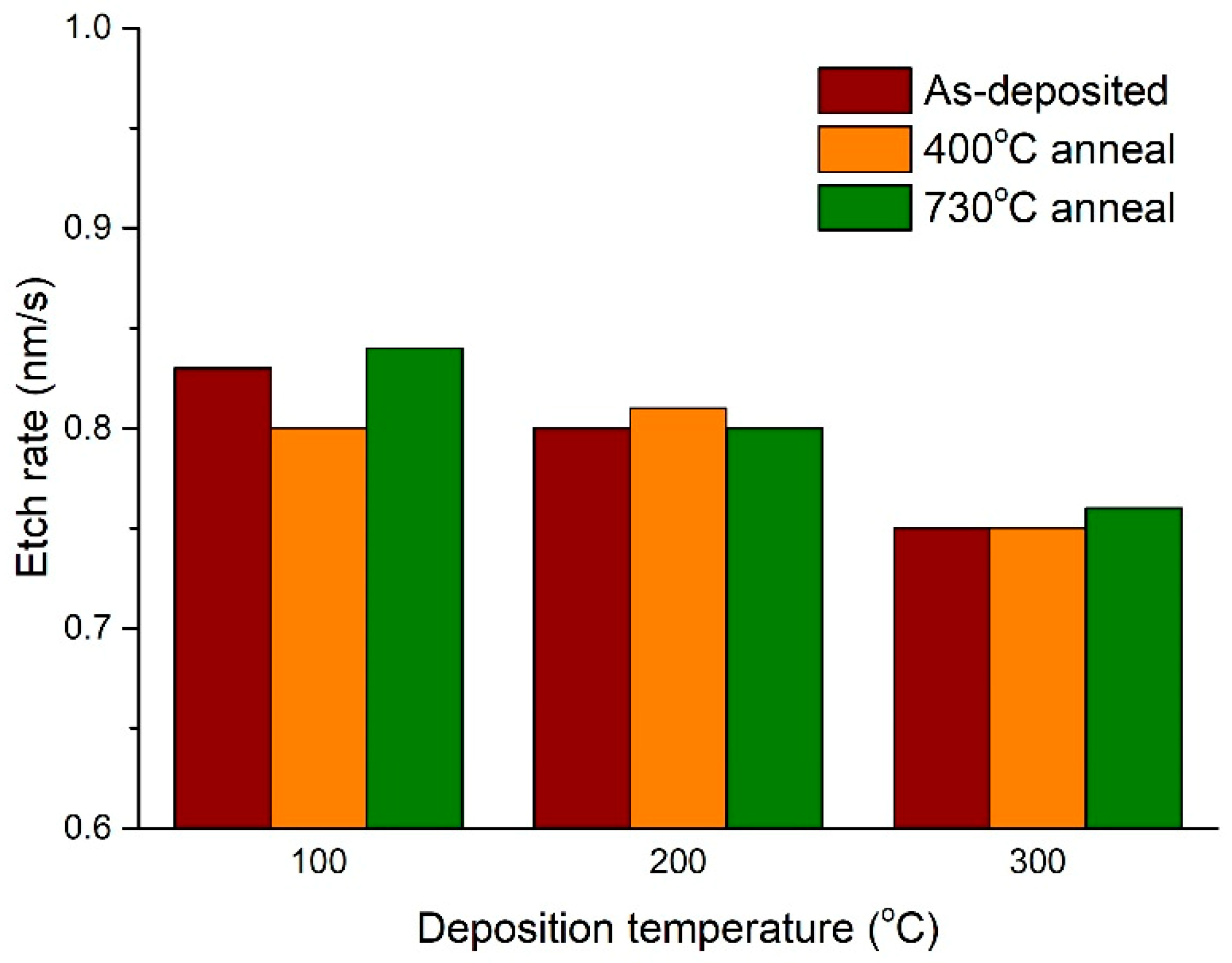
Figure 1 presents the TiO2 dry etch rates on amorphous Al2O3 under different deposition and annealing conditions. The etch rates of samples deposited at 200–300 °C were almost independent of the post-deposition annealing step regardless of the annealing temperature. This indicates that polycrystalline TiO2 deposited over 200 °C is more resistant to reactive species during dry etching than amorphous TiO2 deposited at 100 °C [19]. As a result, the deposition temperature is more important for determining the etch resistance than post-heat treatment. In the case of TiO2 samples deposited at 100 °C, the minimum etch rate was obtained from 400 °C annealing.
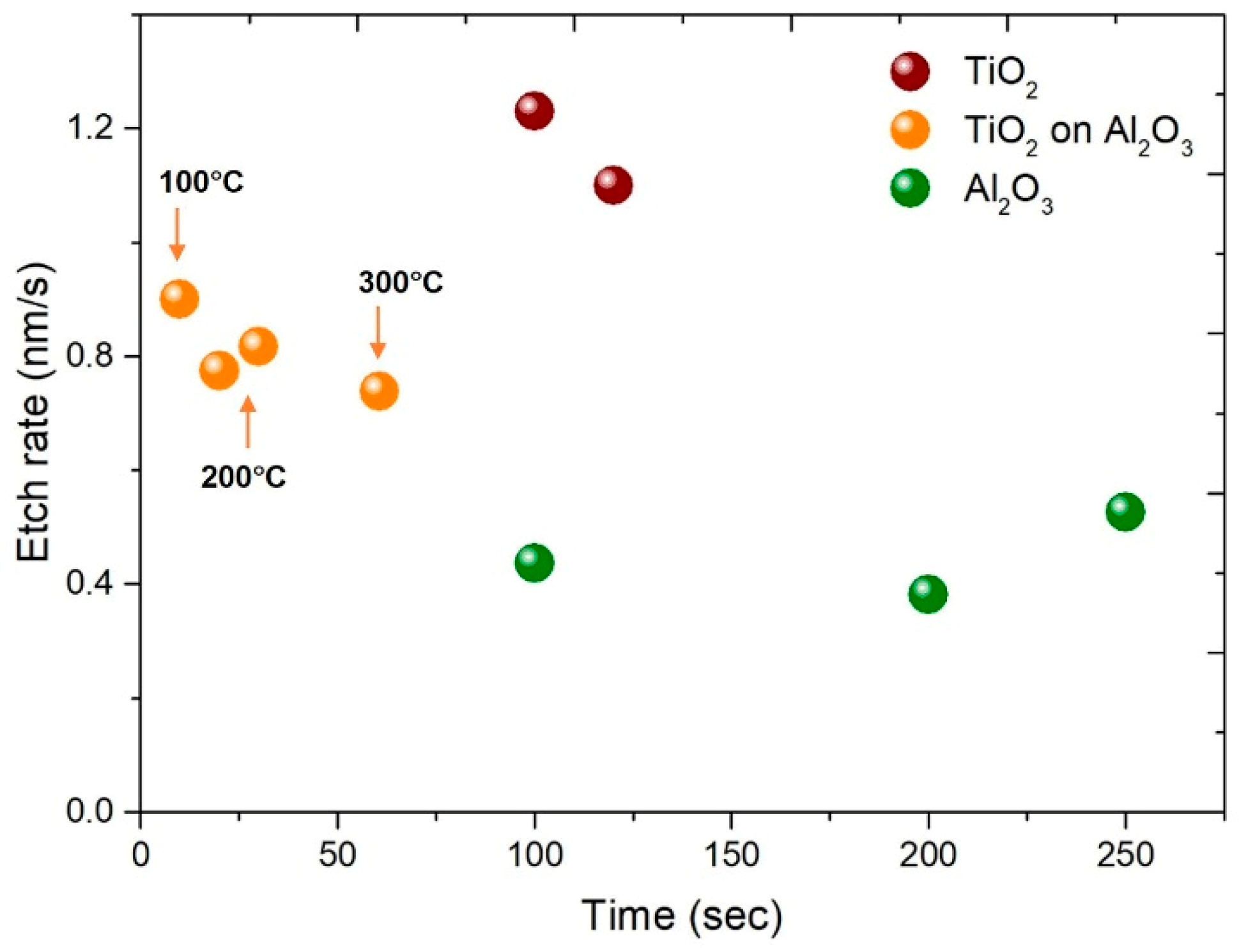
Figure 2 presents the dry etch rates of TiO2 and Al2O3 films as a function of the etch time and deposition temperature. TiO2 and Al2O3 single layers with a thickness of 200 nm were deposited at 200 °C without a post-deposition annealing step, and Figure 2 shows TiO2 layers on Al2O3 deposited at a deposition temperature of 100–300 °C. The selectivity for etching TiO2 over Al2O3 in CHF3 and Ar gas was not remarkable, compared to chemical etching. The dry etch rates of the TiO2 films on Al2O3 were approximately double those of Al2O3 in all samples deposited at different temperature ranges. The etch rates tended to decrease slightly with increasing TiO2 deposition temperature. In the case of a 200-nm-thick TiO2 single layer, the etch rates were 1.1–1.2 nm/s, which were higher than those of the 50 nm-thick TiO2 films on Al2O3. This is because the film density increases with an increasing number of deposition cycles during the ALD process, i.e., with increasing film thickness [20]. Therefore, thicker TiO2 films are more resistant than thinner films. The etch rate of the Al2O3 single layer was almost independent of the etch time.
3.2. Wet Etching
The wet chemical etching process is currently the standard procedure for mass production lines of crystalline silicon solar cells. For example, an alkaline or acidic etching mixture is commonly used for surface texturing; a low concentrated HF solution is used for phosphorus silicon glass removal; an acidic mixture is utilized for edge isolation by single-side etching [21,22]. The pre-cleaning of crystalline silicon wafers is also essential for the elimination of residue and subsequent process homogeneity. Most alkaline cleaning solutions are similar to SC1 in semiconductor processes, and HF dipping is used to clean hydrophilic wafer surfaces. Several cleaning steps have been introduced to further optimize the efficiency potential of PERC-based screen-printed silicon solar cells. Nevertheless, it is important to investigate the etching characteristics because a range of chemical solutions have been developed for these cleaning processes.
Table 1 lists the variation of the etch rates of the TiO2 layer on amorphous Al2O3 in HF, SC1, and SC2 with different concentrations and temperatures. Most films deposited at 300 °C generally showed extremely low etch rates exhibiting overall resistance to chemical etching. The maximum etch rate of TiO2 deposited at 100 °C was 90 nm/min using a 10% HF solution at room temperature. The TiO2 etch rate decreased with decreasing HF concentration, and increased with decreasing deposition and annealing temperature as well as etching temperature. The etch rate in SC1 was half and five times at an etching temperature of 25 °C and 65 °C, respectively, than that in SC2.
3.3. Morphology
For better control and characterization of wet chemical processes, it is important to know not only the etch rate of the solutions, but also the morphological information about the resulting surface as well as its electrical quality. Unlike microelectronics, industrial solar cells commonly have rough surfaces due to anisotropic damage removal or texturing steps. Therefore, it is necessary to examine whether the rough surface restricts the electrical properties compared to a smooth surface [23].
Figure 3 shows top view optical microscopy images of 10-nm-thick Al2O3/40 nm-thick TiO2 stacks deposited at 200–300 °C and annealed in O2 ambient at 400 °C for 30 min before and after etching. From the viewpoint of morphology, there was little difference between the samples deposited at 100 °C and 200 °C (data not shown), but a distinguishable difference was noted at temperatures ranging from 200 °C to 300 °C. This is why Figure 3 related to morphology is focused on the data measured at 200–300 °C. An optical investigation of the stacks examined under a range of conditions suggested that there was no blistering for Al2O3 layers with a thickness of 10 nm. Prior to etching, the sample deposited at 300 °C (Figure 3c) had a rougher surface than any of the other samples and contained non-homogeneous sites caused by surface defects. This layer would not act as a good barrier to prevent etching of the underlying substrate due to the high pinhole density. The smoothest surface was obtained from the sample deposited at 200 °C as shown in Figure 3a.
Wet chemical etching has been used as a tool to produce crystal defects such as dislocations and grain boundaries. Various etching solutions which generate etch pits at dislocations sites have been proven for inorganic materials, allowing an estimation of the dislocation density in the crystal [24]. For this purpose, a 1 wt.% HF solution was used for 2 min at room temperature and yielded different results depending on the deposition temperature.
TiO2 film deposited at 200 °C showed a uniform morphology (Figure 3a), but more small dots with different colors were observed after etching, indicating that the non-uniform thickness of TiO2 results from different local etch rates on the microscale. AFM of the sample deposited at 300 °C (Figure 3c,f) revealed an average roughness, Ra, before HF etching of 0.214 μm, which increased slightly to 0.232 μm after etching. This indicates that the sample deposited at 300 °C in Figure 3c has more inhomogeneity than that at 250 °C, which is likely to have more grain boundaries and a number of etch pits after HF etching as shown in Figure 3f.
3.4. Blistering
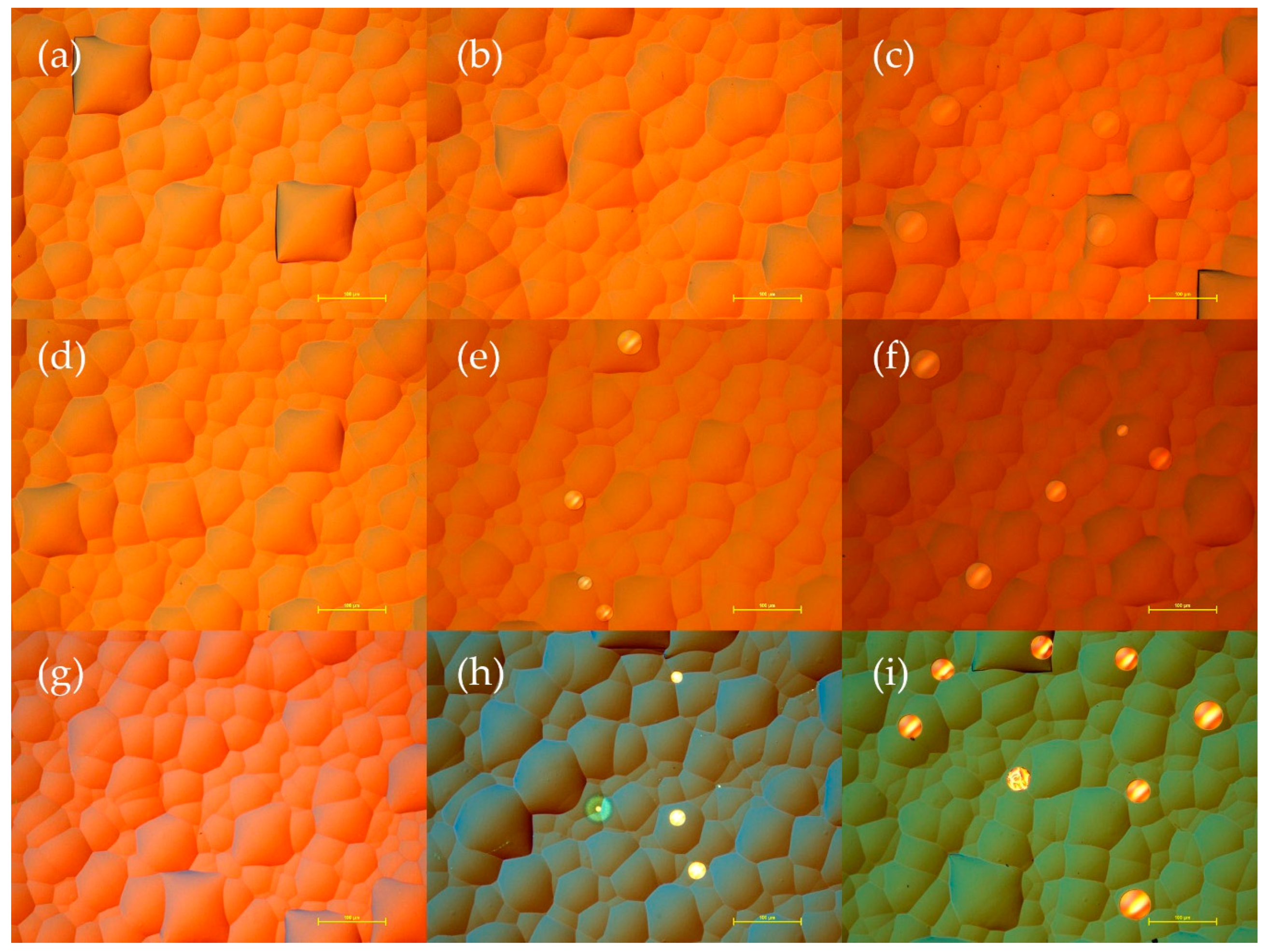
After the post-deposition annealing step, blistering was observed on several samples deposited with a thick Al2O3 single layer or Al2O3/TiO2 stacks. Blisters form when exposed to heat treatment as a result of the accumulation of hydrogen at the Si/Al2O3 interface. Although this has not been fully resolved, the minority carrier lifetime of films exposed to high temperatures is not related directly to the occurrence of macroscopic defects, which are generally known as blisters [25]. These features are located primarily but not exclusively in the grain boundaries as shown in Figure 4. All samples composed of an Al2O3 single layer or Al2O3/TiO2 stacks were deposited at 200 °C and annealed at 400 °C as shown in Figure 4. Figure 5a,b presents SEM images of blistering obtained from Figure 4h,i, respectively.
Typically, depending on the Al2O3 film thickness, the blisters appear as almost perfect circles with a diameter in the range of 1–30 μm, which is much larger than the film thickness. When the Al2O3 film is capped with the TiO2 film, blister formation becomes more prominent. The diameter of the blisters is, however, more dependent on the Al2O3 film thickness rather than TiO2. Several blister size distributions were observed on the samples with the thicker layers. The blisters were similar in size in some cases, but there were different sizes in other cases. Despite this, it was difficult to find a clear correlation between the size distribution and processing conditions. Blisters are present mainly in crystalline grain boundaries, and blister formation is strongly dependent on the surface topology.
For Al2O3 films with thicknesses of less than 10 nm, there were no blisters even when capped with a thick TiO2 layer with a thickness of up to 50 nm. For stacks capped with TiO2, blisters appear in 20-nm-thick Al2O3 films. For example, an Al2O3 single layer more than 30 nm in thickness contained blisters, as did a stack composed of a relatively thinner 20-nm-thick Al2O3 layer capped with a 50-nm-thick TiO2 layer. When an Al2O3 film is thick, the blisters will coalesce and grow over a longer period of time. At a temperature of 200 °C, where atomic layer deposition takes place, the Al2O3 film contains a considerable quantity of hydrogen in the form of OH bonds. After annealing above 500 °C, the hydrogen concentration of the film decreases from an initial value of 10% to 2–3% [26]. This annealing causes the out-diffusion of excessive hydrogen included by atomic layer deposition, which is more predominant in a thin film. In addition, hydrogen may be released during atomic layer deposition due to a reaction between the hydroxyl group in H2O and the titanium precursor, TiCl4, despite the low hydrogen content of approximately 0.4 atom% in the TiO2 film deposited at approximately 200 °C [27,28]. When the TiO2 layer lies on top of the Al2O3 film, the hydrogen is unlikely to diffuse out and accumulates at the point of blister nucleation such as the grain boundaries. Chemical etching of the passivation layers Al2O3/TiO2 is possible, resulting in circular silicon voids approximately the size of the blister.
3.5. Passivation
When limited advanced solar cells among a range of potential cell concepts for commercialization have been introduced to industrial production, one of the major technical challenges is the minimization of passivation degradation after the cleaning processes as well as the preparation of a clean wafer surface prior to the passivation step. Clean surfaces are essential for the passivation of dielectric layers because impurities on the surface can move to the bulk in the subsequent heat treatment steps. The morphology of the samples coated with Al2O3/TiO2 stacks differs according to the post-deposition annealing step due to grain boundaries as shown in Figure 3. Therefore, it is important to examine whether wet chemical etching limits the electrical performance of the annealed samples compared to as-deposited samples.
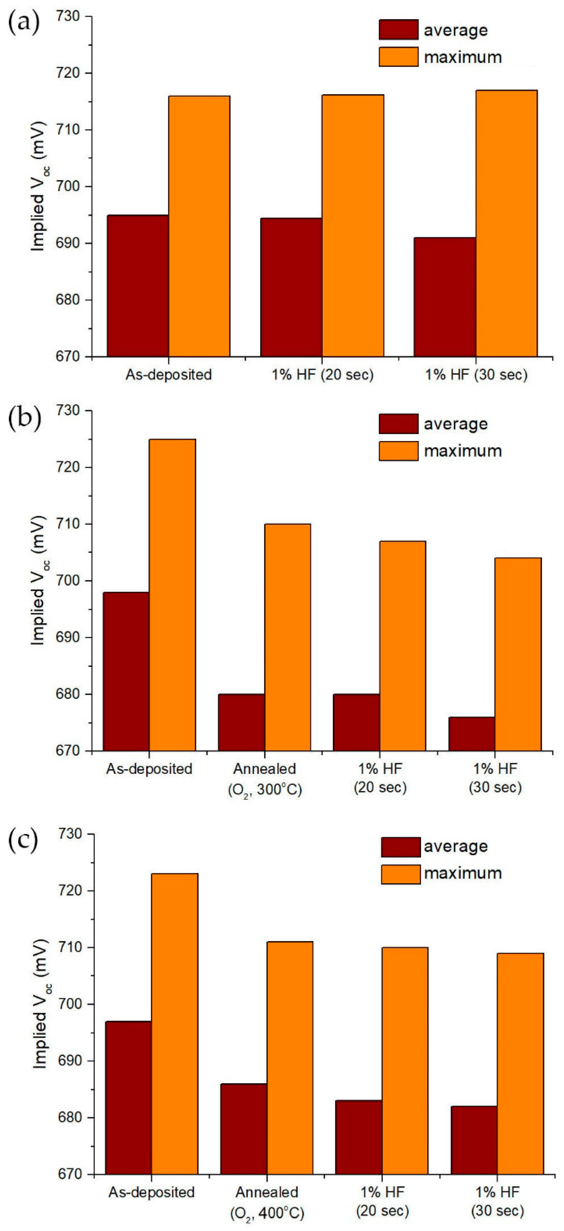
Based on the technique described above, 4 inch diameter wafers passivated with Al2O3/TiO2 stacks were prepared. By measuring the implied open circuit voltage (Voc) at five points including the center position, right and left edges relative to the center, and top and bottom edges, the maximum and average values illustrated the uniformity and quality of passivation over the entire wafer. The results implied open circuit voltage as an etch measure was determined using a quasi-steady state photoconductance (QSSPC) technique at an injection level of Δn = 1 × 1014 cm−3. Figure 6 shows the implied Voc measured on samples passivated by Al2O3/TiO2 stacks deposited at 200 °C after etching with a 1% HF solution in combination with heat treatment at 300–400 °C in O2 ambience. In the case of passivation, the Al2O3 layer in a thermal ALD process has excellent passivation because of the field-effect induced by negative charges when deposited at approximately 200 °C, but not at 100 °C and 300 °C [29]. Well-passivated Al2O3/TiO2 stacks are required because they can be sensitive enough to detect effectively the change in passivation caused by etching. Therefore, it is necessary to examine the effect of etching on the samples deposited at 200 °C with different post-deposition anneal steps in terms of passivation. Compared to the as-deposited sample, the passivation quality of the annealed samples deteriorated as 1% HF etching proceeded. The implied Voc value of the samples annealed at 300 °C decreased by 22 mV, which is more than that annealed at 400 °C after HF etching for 30 s (15 mV). The as-deposited TiO2 sample showed the same maximum implied Voc after wet etching for 30 s while the average values became slightly lower.
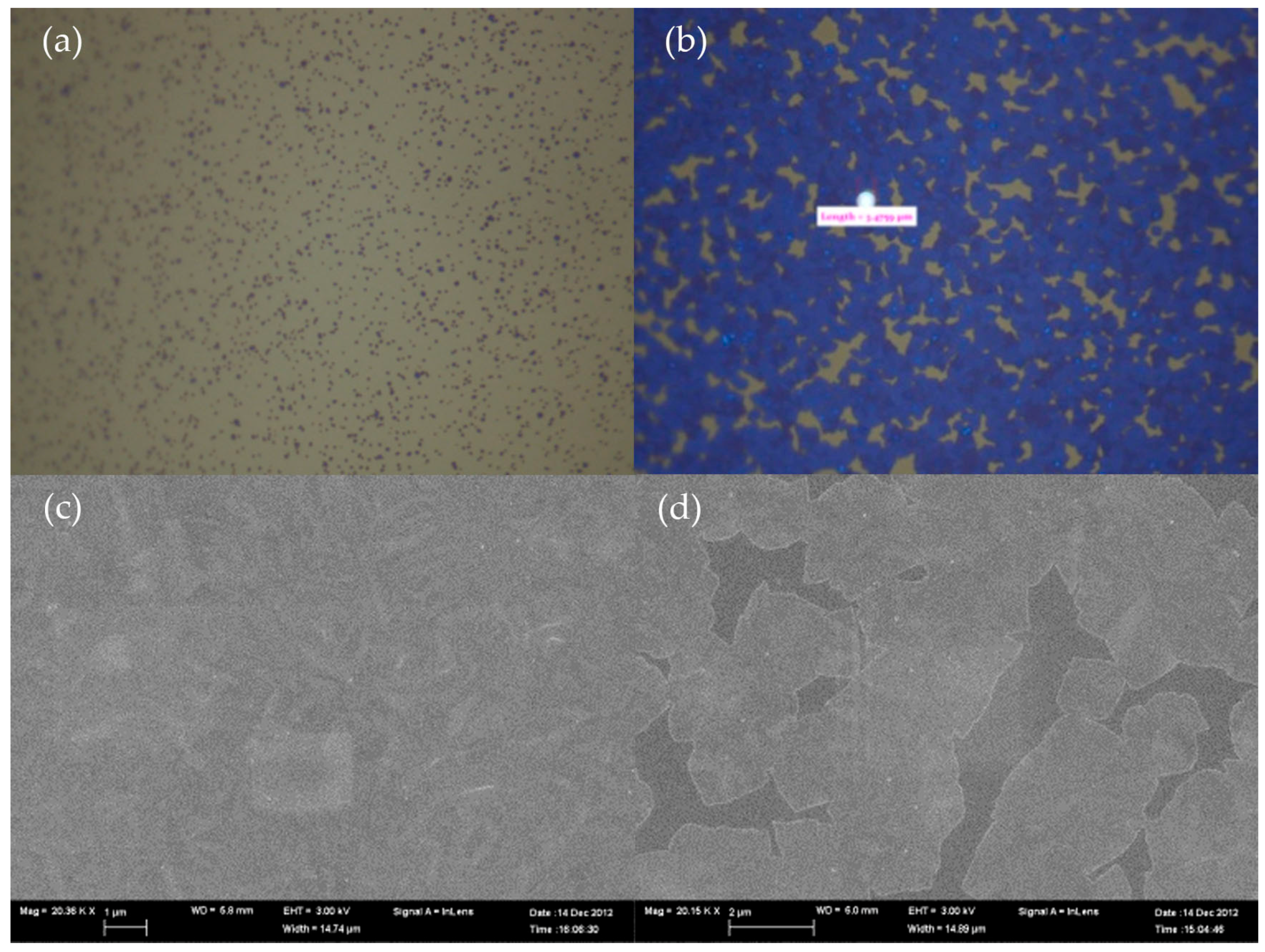
In luminescence imaging of silicon samples passivated by an Al2O3/TiO2 stack after etching with a 1% HF solution as shown in Figure 7, the surface of the sample was excited to emit luminescence and images of luminescent emission were acquired. The following images were calculated using 20 input PL images. Photoluminescence imaging is a fast and convenient method to measure the minority carrier lifetime with high spatial resolution [30]. The as-deposited sample had a relatively more uniform distribution and wider red area indicating a higher lifetime than the annealed samples. In addition, HF etching makes the passivation in the area of wafer edge worse than that in the center. For more information on passivation degradation, optical microscopy was performed on bright and dark areas in the photoluminescence images as shown in Figure 8. The former showed small dots which appear to be an etched area after 1% HF etching, and the latter showed larger dots with different colors, which are likely to have more grain boundaries. The etch resistance of the stack depends on whether the Al2O3 layer is etched at the edges, undercutting the stack, and whether the TiO2 layer contains pinholes (shown in Figure 8b as a white dot), allowing the etching of Al2O3 through the holes.
4. Conclusions
Knowledge of the etch characteristics of dielectric passivation materials is essential because of the integration problem for mass production processes. This paper presented the etch characteristics that modify the passivation quality by removing the capping layer from the Al2O3/TiO2 stacks and including its effects on the morphology. This can be verified by wet etching methods used widely for defect evaluation because of the low cost, simple experimental steps and unconstrained sample geometry.
The chemical etch rate depends mainly on the deposition and annealing temperature, and a higher deposition temperature is beneficial for resisting attack from chemicals including HF and SC solutions. Selecting the appropriate etchant and set of conditions reveals defects because the local etch rate in a defect is different from that in a defect-free region. Post-deposition etching produces etch pits on the solar cell surface due to the non-uniform nature of the defect, resulting in passivation degradation. In terms of the passivation quality, post-deposition heat treatment is ineffective compared to the as-deposited case. The photoluminescence and optical microscopy images showed that there were distinct areas attacked by chemical etching. Therefore, this analysis can be useful in the implementation of alternative passivation stacks for photovoltaic cells.
Funding
This work was supported by the New and Renewable Energy Core Technology Program of the Korea Institute of Energy Technology Evaluation and Planning (KETEP) granted financial from the Ministry of Trade, Industry and Energy, Republic of Korea (No. 20173010012970).
Conflicts of Interest
The author declares no conflict of interest.
References
- Lee, J.; Michaelson, L.; Munoz, K.; Tyson, T.; Gallegos, A.; Sullivan, J.; Buonassisi, T. In-situ photoluminescence imaging for passivation-layer etching process control for photovoltaics. Appl. Phys. Lett. 2014, 105, 043901. [Google Scholar] [CrossRef]
- Deligiannis, D.; Marioleas, V.; Vasudevan, R.; Visser, C.C.; van Swaaij, R.A.; Zeman, M. Understanding the thickness-dependent effective lifetime of crystalline silicon passivated with a thin layer of intrinsic hydrogenated amorphous silicon using a nanometer-accurate wet-etching method. J. Appl. Phys. 2016, 119, 235307. [Google Scholar] [CrossRef]
- Rahman, T.; To, A.; Pollard, M.E.; Grant, N.E.; Colwell, J.; Payne, D.N.; Murphy, J.D.; Bagnall, D.M.; Hoex, B.; Boden, S.A. Minimising bulk lifetime degradation during the processing of interdigitated back contact silicon solar cells. Prog. Photovolt. Res. Appl. 2018, 26, 38–47. [Google Scholar] [CrossRef]
- Dullweber, T.; Schmidt, J. Industrial silicon solar cells applying the passivated emitter and rear cell (PERC) concept—A review. IEEE J. Photovolt. 2016, 6, 1366–1381. [Google Scholar] [CrossRef]
- Cornagliotti, E.; Uruena, A.; Horzel, J. How much rear side polishing is required? A study on the impact of rear side polishing in PERC solar cells. In Proceedings of the 27th European Photovoltaic Solar Energy Conference and Exhibition, Frankfurt, Germany, 24–28 September 2012; pp. 561–566. [Google Scholar]
- Huang, H.; Lv, J.; Bao, Y.; Xuan, R.; Sun, S.; Sneck, S.; Li, S.; Modanese, C.; Savin, H.; Wang, A. 20.8% industrial PERC solar cell: ALD Al2O3 rear surface passivation, efficiency loss mechanisms analysis and roadmap to 24%. Sol. Energy Mater. Sol. Cells 2017, 161, 14–30. [Google Scholar] [CrossRef]
- Suh, D.; Weber, K. Effective silicon surface passivation by atomic layer deposited Al2O3/TiO2 stacks. Phys. Status Solidi (RRL) Rapid Res. Lett. 2014, 8, 40–43. [Google Scholar] [CrossRef]
- Suh, D.; Choi, D.-Y.; Weber, K.J. Al2O3/TiO2 stack layers for effective surface passivation of crystalline silicon. J. Appl. Phys. 2013, 114, 154107. [Google Scholar] [CrossRef]
- Vermang, B.; Goverde, H.; Uruena, A.; Lorenz, A.; Cornagliotti, E.; Rothschild, A.; John, J.; Poortmans, J.; Mertens, R. Blistering in ALD Al2O3 passivation layers as rear contacting for local Al BSF Si solar cells. Sol. Energy Mater. Sol. Cells 2012, 101, 204–209. [Google Scholar] [CrossRef]
- Vermang, B.; Goverde, H.; Lorenz, A.; Uruena, A.; Vereecke, G.; Meersschaut, J.; Cornagliotti, E.; Rothschild, A.; John, J.; Poortmans, J. On the blistering of atomic layer deposited Al2O3 as Si surface passivation. In Proceedings of the 2011 37th IEEE Photovoltaic Specialists Conference, Seattle, WA, USA, 13 June 2011; pp. 003562–003567. [Google Scholar]
- Richter, A.; Henneck, S.; Benick, J.; Hörteis, M.; Hermle, M.; Glunz, S. Firing stable Al2O3/SiNx layer stack passivation for the front side boron emitter of n-type silicon solar cells. In Proceedings of the 25th European Photovoltaic Solar Energy Conference and Exhibition, Valencia, Spain, 6–9 September 2010; pp. 1453–1456. [Google Scholar]
- Kania, D.; Saint-Cast, P.; Hofmann, M.; Rentsch, J.; Preu, R. High temperature stability of PECVD aluminium oxide layers applied as negatively charged passivation on c-Si surfaces. In Proceedings of the 25th European Photovoltaic Solar Energy Conference, Valencia, Spain, 6–9 September 2010; pp. 2292–2296. [Google Scholar]
- Sperlich, H.; Decker, D.; Saint-Cast, P.; Erben, E.; Peters, L. High productive Solar Cell Passivation on Roth&Rau MAiA® MW-PECVD inline machine—A comparison of Al2O3, SiO2 and SiNx-H process conditions and performance. In Proceedings of the 25th European Photovoltaic Solar Energy Conference and Exhibition, Valencia, Spain, 6–9 September 2010; pp. 1352–1357. [Google Scholar]
- Gardner, D.S.; Flinn, P.A. Mechanical stress as a function of temperature in aluminum films. IEEE Trans. Electron Devices 1988, 35, 2160–2169. [Google Scholar] [CrossRef]
- Dingemans, G.; Van de Sanden, M.; Kessels, W. Influence of the deposition temperature on the c-Si surface passivation by Al2O3 films synthesized by ALD and PECVD. Electrochem. Solid-State Lett. 2010, 13, H76–H79. [Google Scholar] [CrossRef]
- Kern, W. Handbook of Semiconductor Wafer Cleaning Technology; Noyes Publication: Saddle River, NJ, USA, 1993; pp. 111–196. [Google Scholar]
- Sinton, R.; Macdonald, D. WCT-120 Photoconductance Lifetime Tester: User Manual; Sinton Consulting: Boulder, CO, USA, 2006. [Google Scholar]
- Chen, D.; Edwards, M.; Wenham, S.; Abbott, M.; Hallam, B. Laser enhanced gettering of silicon substrates. Front. Energy 2017, 11, 23–31. [Google Scholar] [CrossRef]
- Aarik, J.; Aidla, A.; Kiisler, A.-A.; Uustare, T.; Sammelselg, V. Effect of crystal structure on optical properties of TiO2 films grown by atomic layer deposition. Thin Solid Films 1997, 305, 270–273. [Google Scholar] [CrossRef]
- Kim, S.K.; Choi, G.J.; Kim, J.H.; Hwang, C.S. Growth behavior of Al-doped TiO2 thin films by atomic layer deposition. Chem. Mater. 2008, 20, 3723–3727. [Google Scholar] [CrossRef]
- Vazsonyi, E.; De Clercq, K.; Einhaus, R.; Van Kerschaver, E.; Said, K.; Poortmans, J.; Szlufcik, J.; Nijs, J. Improved anisotropic etching process for industrial texturing of silicon solar cells. Sol. Energy Mater. Sol. Cells 1999, 57, 179–188. [Google Scholar] [CrossRef]
- Hauser, A.; Hahn, G.; Spiegel, M.; Fath, P.; Bucher, E.; Feist, H.; Breitenstein, O.; Rakotoniaina, J.P. Comparison of different techniques for edge isolation. In Proceedings of the 17th European photovoltaic solar energy conference, Munich, Germany, 22–26 October 2001; pp. 1739–1742. [Google Scholar]
- De Wolf, S.; Agostinelli, G.; Beaucarne, G.; Vitanov, P. Influence of stoichiometry of direct plasma-enhanced chemical vapor deposited SiNx films and silicon substrate surface roughness on surface passivation. J. Appl. Phys. 2005, 97, 063303. [Google Scholar] [CrossRef]
- Souriau, L.; Terzieva, V.; Meuris, M.; Caymax, M. A Wet Etching Technique to Reveal Threading Dislocations in Thin Germanium Layers. Solid State Phenomena 2008, 134, 83–86. [Google Scholar] [CrossRef]
- Hennen, L.; Granneman, E.; Kessels, W. Analysis of blister formation in spatial ALD Al2O3 for silicon surface passivation. In Proceedings of the 38th IEEE Photovoltaic Specialists Conference, Austin, TX, USA, 3–8 June 2012; pp. 001049–001054. [Google Scholar]
- Granneman, E.H.; Kuznetsov, V.I.; Vermont, P. Spatial ALD, Deposition of Al2O3 Films at Throughputs Exceeding 3000 Wafers per Hour. ECS Trans. 2014, 61, 3–16. [Google Scholar] [CrossRef]
- Matero, R.; Rahtu, A.; Ritala, M. In situ quadrupole mass spectrometry and quartz crystal microbalance studies on the atomic layer deposition of titanium dioxide from titanium tetrachloride and water. Chem. Mater. 2001, 13, 4506–4511. [Google Scholar] [CrossRef]
- Ferguson, J.; Yoder, A.; Weimer, A.; George, S. TiO2 atomic layer deposition on ZrO2 particles using alternating exposures of TiCl4 and H2O. Appl. Surf. Sci. 2004, 226, 393–404. [Google Scholar] [CrossRef]
- Puurunen, R.L. Surface chemistry of atomic layer deposition: A case study for the trimethylaluminum/water process. J. Appl. Phys. 2005, 97, 9. [Google Scholar] [CrossRef]
- Keller, P.; Zuschlag, A.; Karzel, P.; De Moro, F.; Hahn, G. Defect characterization and investigation of RST-silicon ribbon wafers. In Proceedings of the 28th European Photovoltaic Solar Energy Conference and Exhibition, Paris, France, 30 September–4 October 2013; pp. 1512–1517. [Google Scholar]
Figure 1.
TiO2 dry etch rates on amorphous Al2O3 as a function of the deposition temperature under different annealing conditions.
Figure 1.
TiO2 dry etch rates on amorphous Al2O3 as a function of the deposition temperature under different annealing conditions.

Figure 2.
Dry etch rates of TiO2 (in types of single layer and stack) and Al2O3 single layer as a function of the etching time. The TiO2 deposition temperatures of stack samples are also presented.
Figure 2.
Dry etch rates of TiO2 (in types of single layer and stack) and Al2O3 single layer as a function of the etching time. The TiO2 deposition temperatures of stack samples are also presented.

Figure 3.
Optical microscopy images of TiO2 layer deposited at (a,d) 200 °C, (b,e) 250 °C and (c,f) 300 °C on an amorphous Al2O3 layer: images (a–c) were obtained before etching and (d–f) after etching. The insets in (c) and (f) are AFM images used for the surface roughness measurements.
Figure 3.
Optical microscopy images of TiO2 layer deposited at (a,d) 200 °C, (b,e) 250 °C and (c,f) 300 °C on an amorphous Al2O3 layer: images (a–c) were obtained before etching and (d–f) after etching. The insets in (c) and (f) are AFM images used for the surface roughness measurements.
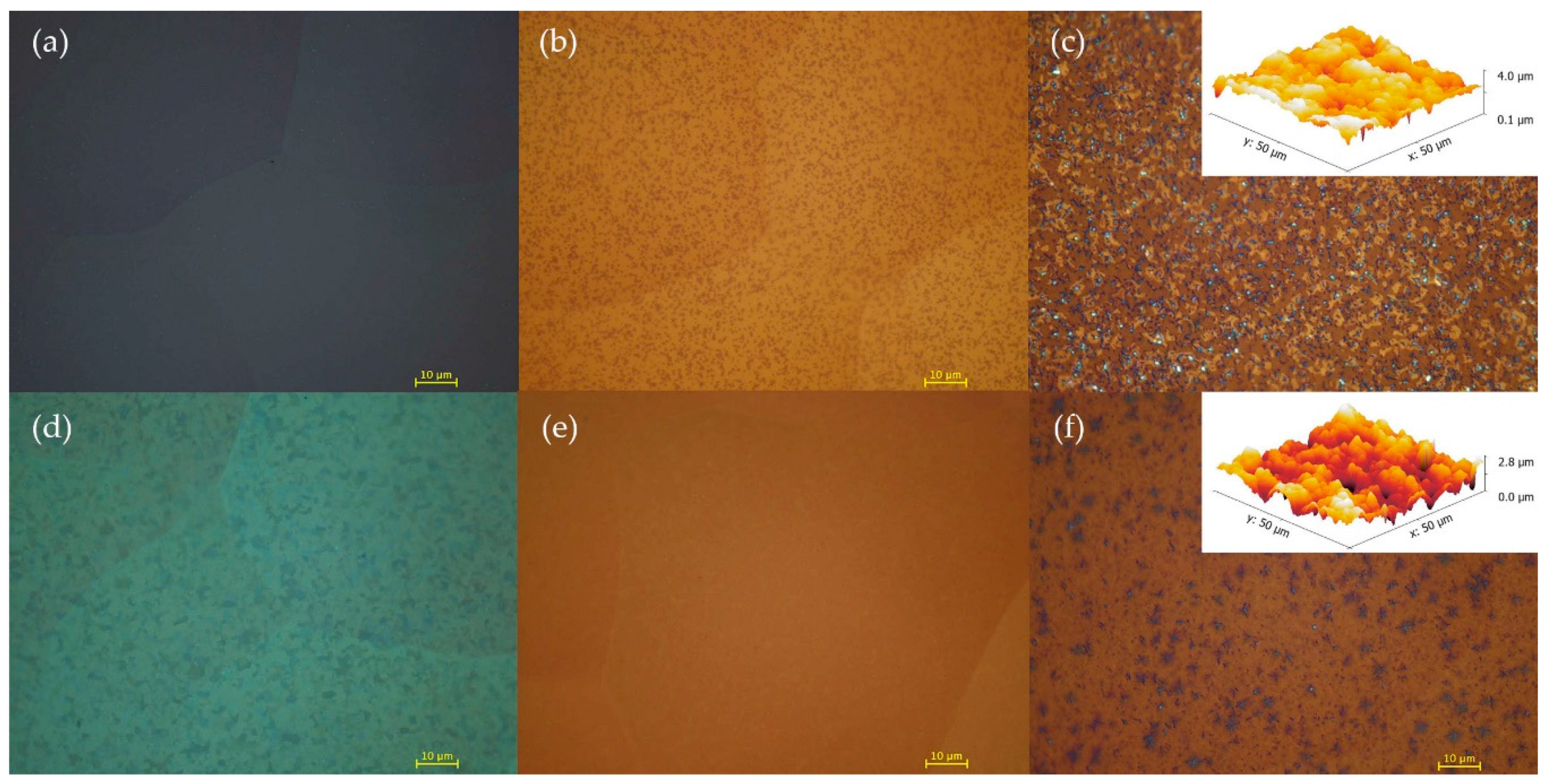
Figure 4.
Optical microscopy images of the samples passivated by Al2O3 and/or TiO2 layers: (a–c) Al2O3 single layer, (d–f) 20-nm-thick and (g–i) 50-nm-thick TiO2 on Al2O3 layer. Samples (a,d,g) have a 10-nm-thick Al2O3 layer, (b,e,h) 20-nm-thick layer and (c,f,i) 30-nm-thick layer. The scale bars represent 100 μm.

Figure 5.
SEM images of the samples passivated by Al2O3/TiO2: images (a) and (b) were obtained from Figure 4h,i, respectively. The scale bars represents 1 μm.
Figure 5.
SEM images of the samples passivated by Al2O3/TiO2: images (a) and (b) were obtained from Figure 4h,i, respectively. The scale bars represents 1 μm.
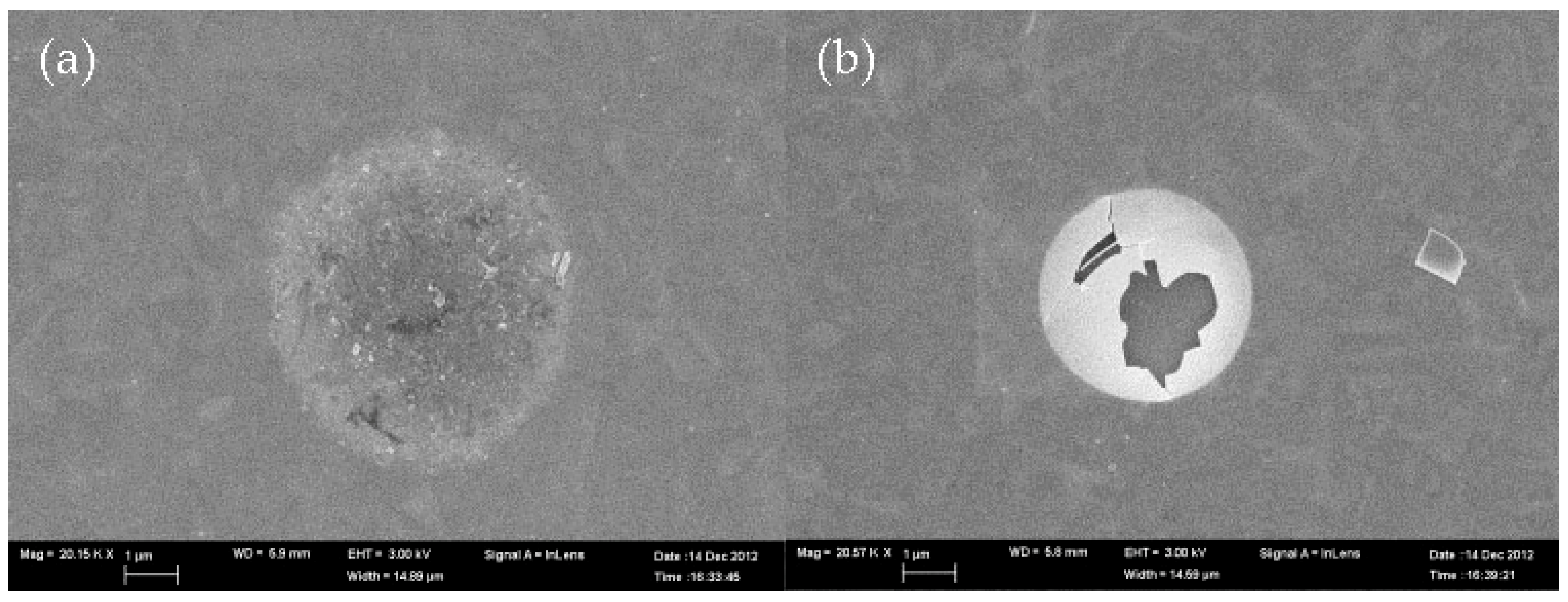
Figure 6.
Implied open circuit voltage of samples passivated by the Al2O3/TiO2 stack after etching with a 1% HF solution: (a) no annealing and (b,c) 300 °C and 400 °C annealing in O2 ambient.
Figure 6.
Implied open circuit voltage of samples passivated by the Al2O3/TiO2 stack after etching with a 1% HF solution: (a) no annealing and (b,c) 300 °C and 400 °C annealing in O2 ambient.

Figure 7.
Photoluminescence images of the samples passivated by Al2O3/TiO2 stack after 1% HF etching for 30 s: (a) no annealing and (b,c) 300 °C and 400 °C annealing in O2 ambient.
Figure 7.
Photoluminescence images of the samples passivated by Al2O3/TiO2 stack after 1% HF etching for 30 s: (a) no annealing and (b,c) 300 °C and 400 °C annealing in O2 ambient.
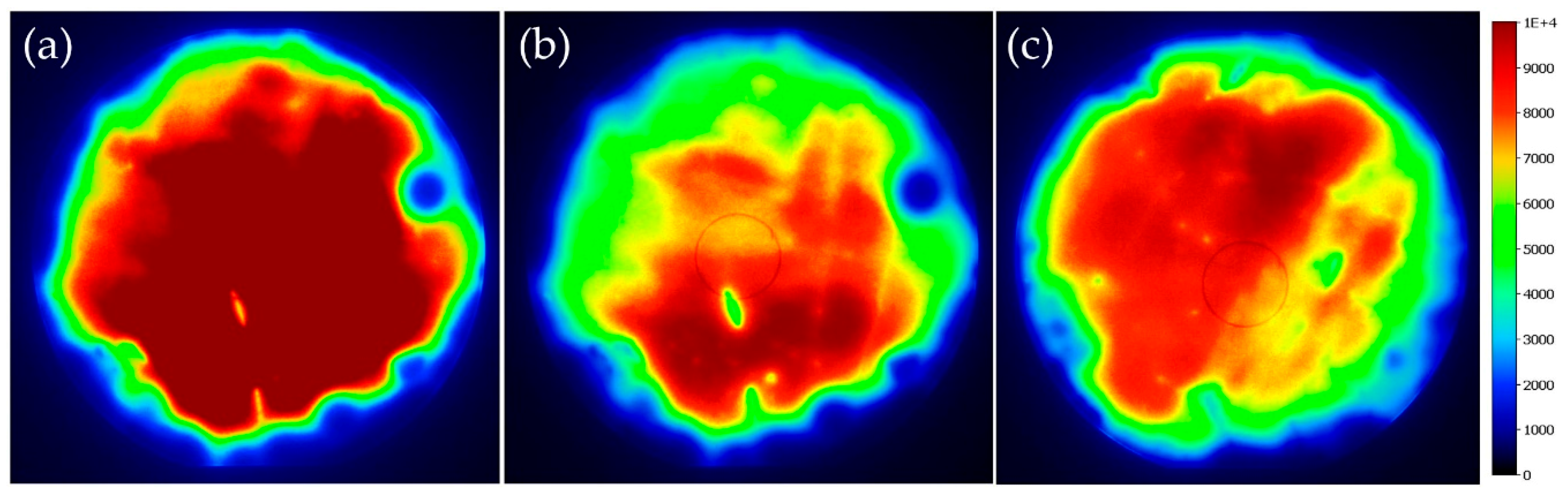
Figure 8.
Optical microscopy images of samples passivated by Al2O3/TiO2 stack after 1% HF etching for 30 s: (a) bright and (b) dark area in photoluminescence. (c,d) isSEM images of (a,b), respectively. (b) The pinhole has a diameter of 3.48 μm and (c,d) the scale bars represent 2 μm.
Figure 8.
Optical microscopy images of samples passivated by Al2O3/TiO2 stack after 1% HF etching for 30 s: (a) bright and (b) dark area in photoluminescence. (c,d) isSEM images of (a,b), respectively. (b) The pinhole has a diameter of 3.48 μm and (c,d) the scale bars represent 2 μm.


Table 1.
Wet etch rate to several chemical solutions as a function of the deposition temperature under different annealing conditions.
Table 1.
Wet etch rate to several chemical solutions as a function of the deposition temperature under different annealing conditions.
| Tdep (°C) | Tann (°C) | Etch Rate (nm/min) | |||||
|---|---|---|---|---|---|---|---|
| HF (25 °C) | SC1 | SC2 | |||||
| 1% | 10% | 25 °C | 65 °C | 25 °C | 65 °C | ||
| 100 | - | 1.1 ± 0.17 | 90.0 ± 13 | 0.29 ± 0.09 | 15.0 ± 1.4 | 0.56 ± 0.04 | 3.0 ± 1.4 |
| 400 | no etch | scratched | no etch | no etch | no etch | no etch | |
| 730 | no etch | no etch | no etch | no etch | no etch | no etch | |
| 200 | - | 1.0 ± 0.07 | 87.0 ± 7.8 | 0.1 ± 0.01 | 13.0 ± 1.0 | 0.52 ± 0.13 | 2.8 ± 0.8 |
| 400 | no etch | no etch | no etch | no etch | no etch | no etch | |
| 730 | |||||||
| 300 | - | no etch | no etch | no etch | no etch | no etch | no etch |
| 400 | |||||||
| 730 | |||||||
© 2019 by the author. Licensee MDPI, Basel, Switzerland. This article is an open access article distributed under the terms and conditions of the Creative Commons Attribution (CC BY) license (http://creativecommons.org/licenses/by/4.0/).
Share and Cite
MDPI and ACS Style
Suh, D. Etch Characteristics and Morphology of Al2O3/TiO2 Stacks for Silicon Surface Passivation. Sustainability 2019, 11, 3857. https://doi.org/10.3390/su11143857
AMA Style
Suh D. Etch Characteristics and Morphology of Al2O3/TiO2 Stacks for Silicon Surface Passivation. Sustainability. 2019; 11(14):3857. https://doi.org/10.3390/su11143857
Chicago/Turabian StyleSuh, Dongchul. 2019. "Etch Characteristics and Morphology of Al2O3/TiO2 Stacks for Silicon Surface Passivation" Sustainability 11, no. 14: 3857. https://doi.org/10.3390/su11143857
Note that from the first issue of 2016, this journal uses article numbers instead of page numbers. See further details here.