
Reactions in Electrodeposited Cu/Sn and Cu/Ni/Sn Nanoscale Multilayers for Interconnects

Abstract
:1. Introduction
2. Results
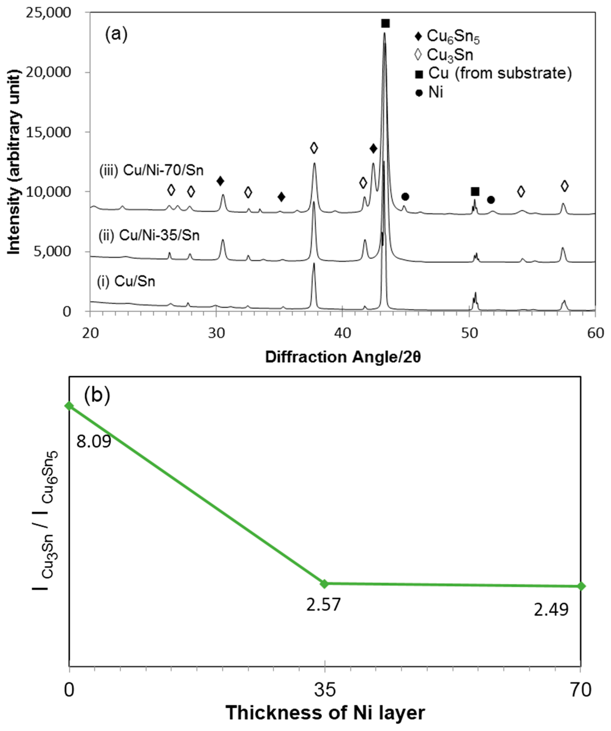
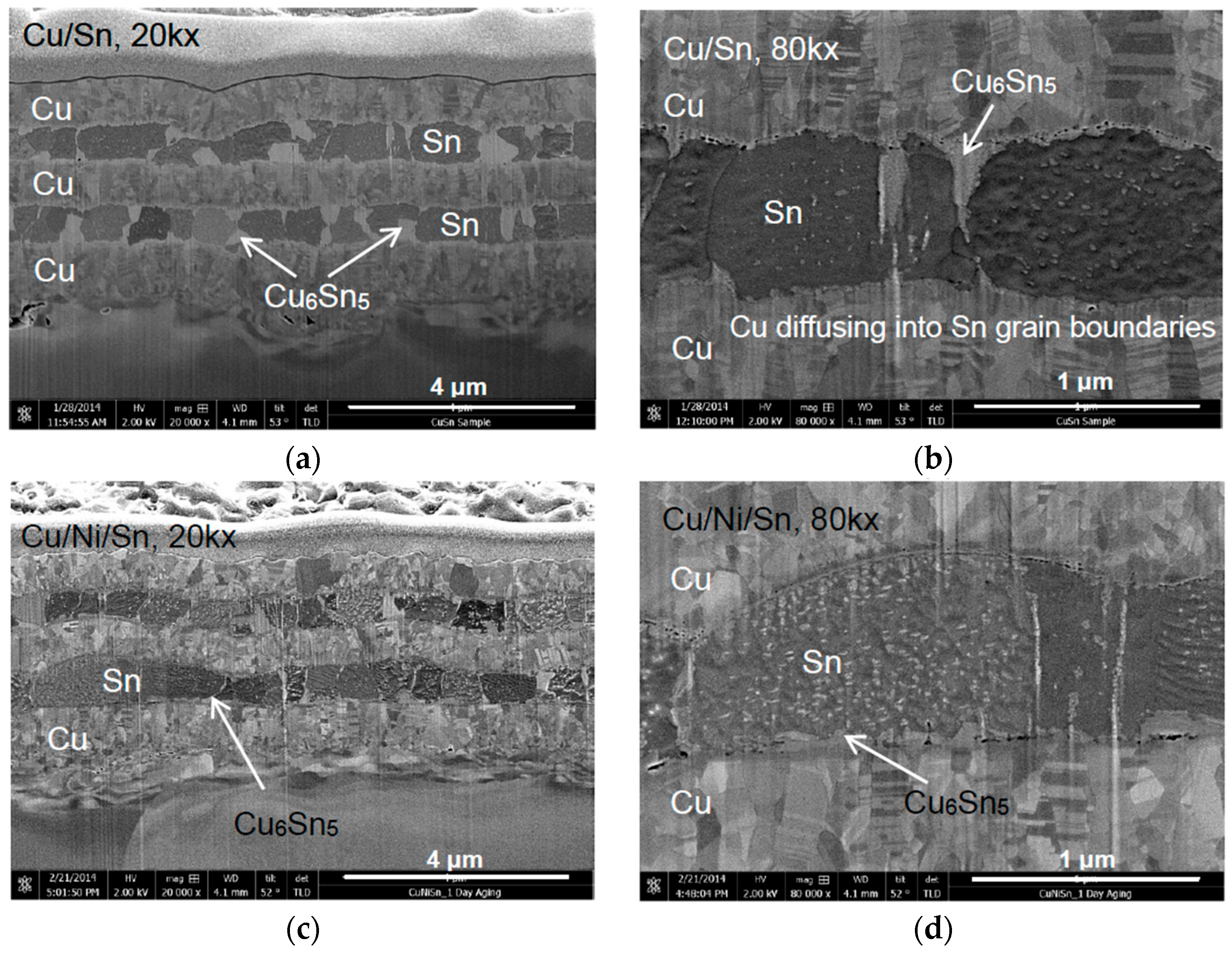
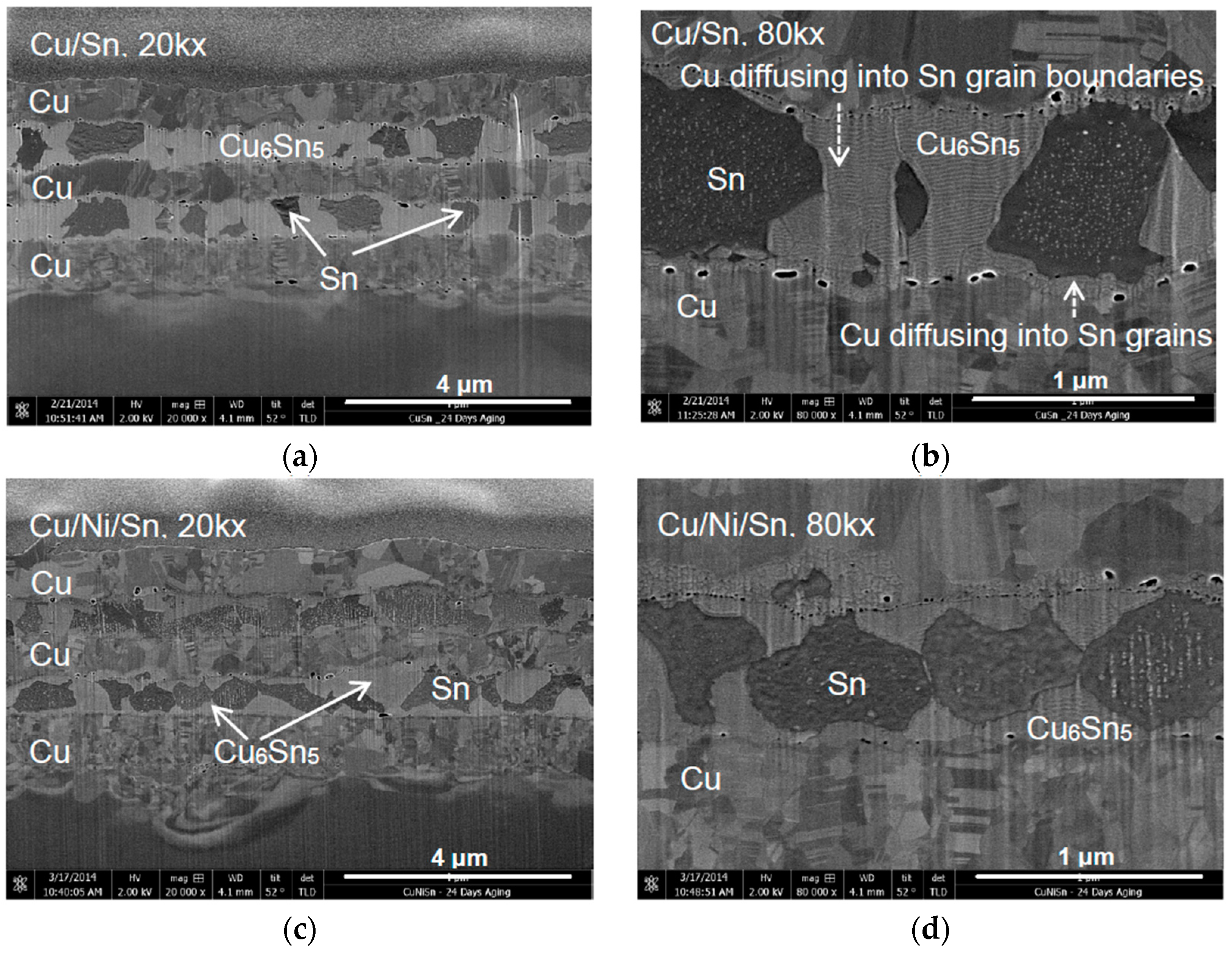
2.1. Solid State Reactions of Cu/Sn and Cu/Ni/Sn Multilayers
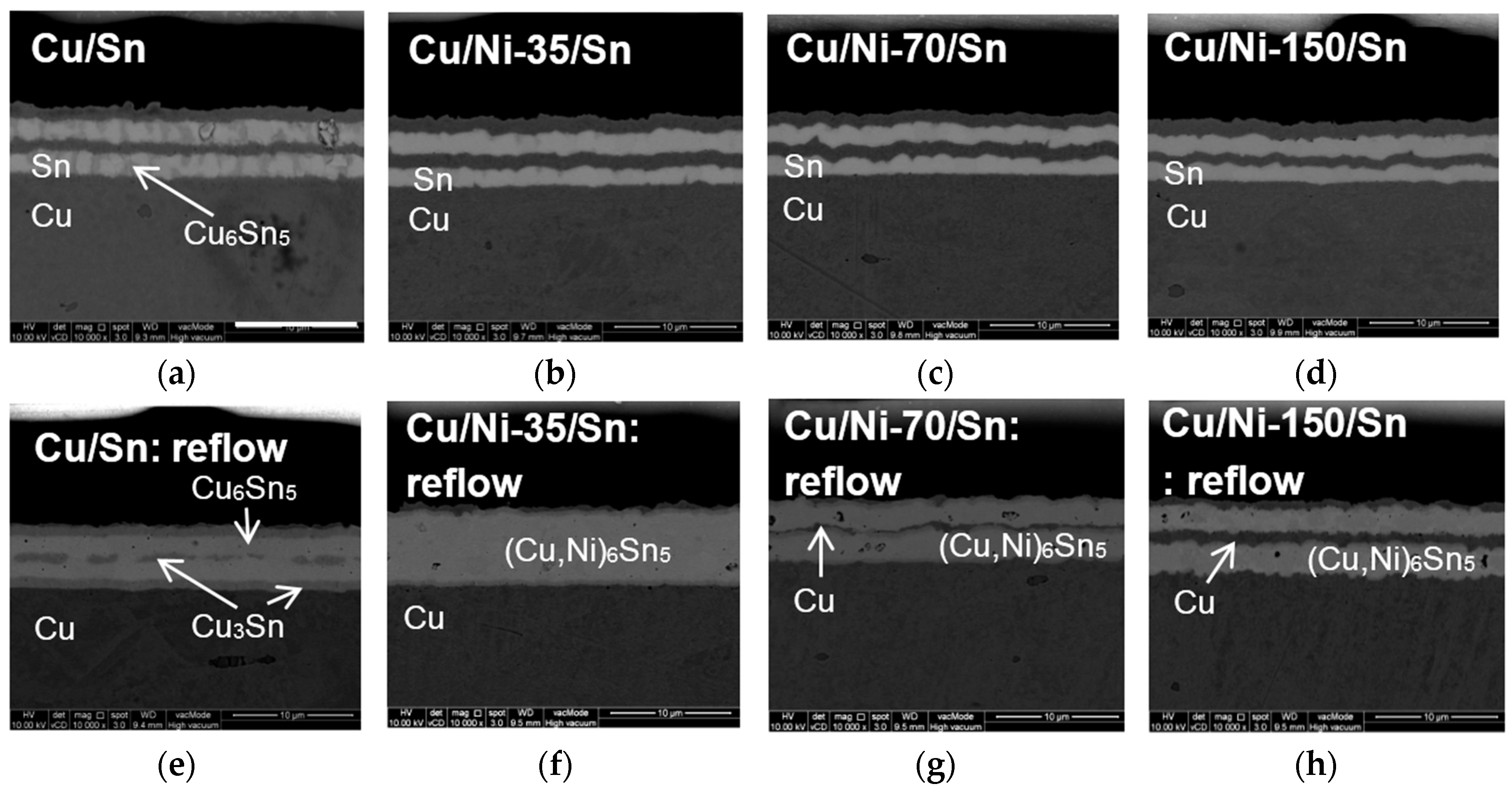
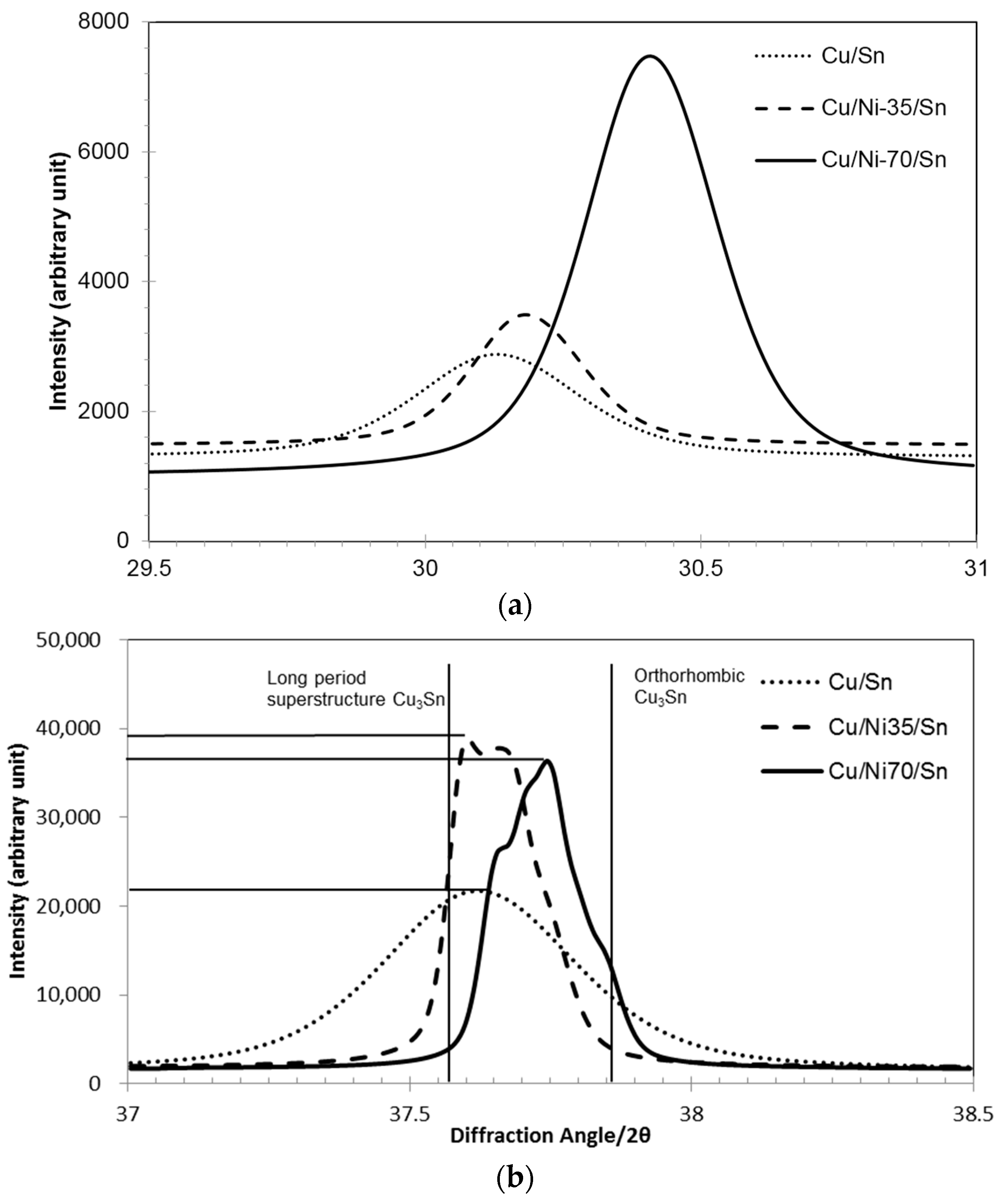
2.2. Solid-Liquid State Reactions of Cu/Sn and Cu/Ni/Sn Multilayers
2.2.1. Short Reflow
2.2.2. Long Reflow
3. Discussion
3.1. IMC Formation during Solid State Reactions
3.2. IMC Formation during Solid Liquid State Reactions
3.2.1. Dissolution of Ni during Reflow
3.2.2. Effect of Ni Addition in Cu6Sn5 IMC
3.2.3. Substitution of Ni Atoms in Cu Lattice in Cu3Sn IMC
4. Materials and Methods
5. Conclusions
- In the electrodeposited Cu/Sn system, Cu6Sn5 IMC is seen to grow even after one day of room temperature aging, while less Cu-Sn IMC is found in Cu/Ni/Sn system under the same conditions. This finding is important to prevent premature intermixing between the multilayers prior to reflowing during manufacturing process.
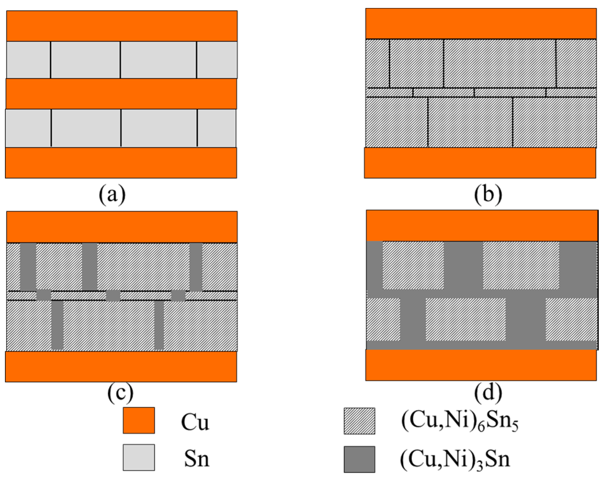
- During solid state reaction in the Cu/Sn system, the growth of the Cu6Sn5 first started through rapid reaction at the Cu/Sn interface followed by grain boundary diffusion of Cu atoms into the Sn grain boundaries. With the addition of Ni in between Cu and Sn, Ni atoms are suggested to block the diffusion path of Cu atoms into Sn grain boundaries and slow down IMC formation.
- During liquid solid reaction, at 70 nm thickness Ni dissolution is incomplete in the Cu/Ni/Sn multilayers. Thus, to achieve homogeneous IMC layer during short reflow, Ni thickness less than 70 nm is recommended. The addition of Ni suppresses formation of Cu3Sn IMC, regardless of the thickness of the Ni layers.
- After 60 min of long reflow, Cu/Sn multilayers have been transformed totally into Cu3Sn. In the Cu/Ni/Sn system, Ni atoms take part in the formation of (Cu,Ni)6Sn5 and, thus, stabilizes the IMC and retards transformation into (Cu,Ni)3Sn. Formation of (Cu,Ni)3Sn is suspected to be due to the limited Sn supply in the system.
- The mechanical properties of the unique “brick-wall” morphology of the [(Cu,Ni)6Sn5 + (Cu,Ni)3Sn] composite formed in the Cu/Ni-70/Sn samples after long reflow would be interesting, as it may influence fracture propagation.
Acknowledgments
Author Contributions
Conflicts of Interest
References
- Agarwal, R.; Zhang, W.; Limaye, P.; Labie, R.; Dimcic, B.; Phommahaxay, A.; Soussan, P. Cu/Sn Microbumps Interconnect for 3D TSV Chip Stacking. In Proceedings of the Electronic Components and Technology Conference, Las Vegas, NV, USA, 1–4 June 2010.
- Yoon, K.S.; Yoo, S.; Shin, Y.S.; Han, M.K.; Lee, C.W. Joint Properties of Solder Capped Copper Pillars for 3D Packaging. In Proceedings of the Electronic Components and Technology Conference, Las Vegas, NV, USA, 1–4 June 2010.
- Tay, S.L.; Haseeb, A.S.M.A.; Johan, M.R.; Munroe, P.R.; Quadir, M.Z. Influence of Ni nanoparticle on the morphology and growth of interfacial intermetallic compounds between Sn3.8Ag0.7Cu lead-free solder and copper substrate. Intermetallics 2013, 33, 8–15. [Google Scholar] [CrossRef]
- Wang, Y.W.; Chang, C.C.; Kao, C.R. Minimum effective Ni addition to SnAgCu solders for retarding Cu3Sn growth. J. Alloys Compd. 2009, 478, L1–L4. [Google Scholar] [CrossRef]
- Gao, F.; Takemoto, T.; Nishikawa, H. Effects of Co and Ni addition on reactive diffusion between Sn–3.5Ag solder and Cu during soldering and annealing. Mater. Sci. Eng. A 2006, 420, 39–46. [Google Scholar] [CrossRef]
- Nogita, K.; Nishimura, T. Nickel-stabilized hexagonal (Cu,Ni)6Sn5 in Sn–Cu–Ni lead-free solder alloys. Scr. Mater. 2008, 59, 191–194. [Google Scholar] [CrossRef]
- Subramaniam, K.N. Reliability of lead-free electronic solder interconnects: Roles of materials and service parameters. In Lead-Free Solders: Materials Reliability for Electronics; Subramaniam, K.N., Ed.; John Wiley and Sons Ltd.: Chichester, UK, 2012; pp. 281–304. [Google Scholar]
- Tsukamoto, H.; Dong, Z.; Huang, H.; Nishimura, T.; Nogita, K. Nanoindentation characterization of intermetallic compounds formed between Sn–Cu (–Ni) ball grid arrays and Cu substrates. Mater. Sci. Eng. B 2009, 164, 44–50. [Google Scholar] [CrossRef]
- Xu, L.; Pang, J.H.L. Nano-indentation characterization of Ni–Cu–Sn IMC layer subject to isothermal aging. Thin Solid Films 2006, 504, 362–366. [Google Scholar] [CrossRef]
- Jang, G.Y.; Lee, J.W.; Duh, J.G. The nanoindentation characteristics of Cu6Sn5, Cu3Sn, and Ni3Sn4 intermetallic compounds in the solder bump. J. Electron. Mater. 2004, 33, 1103–1110. [Google Scholar] [CrossRef]
- Mu, D.; Huang, H.; Mcdonald, S.D.; Nogita, K. Creep and mechanical properties of Cu6Sn5 and (Cu,Ni)6Sn5 at Elevated Temperatures. J. Electron. Mater. 2013, 42, 304–311. [Google Scholar] [CrossRef]
- Tu, K.N. Interdiffusion and reaction in bimetallic Cu-Sn thin films. Acta Metall. 1973, 21, 347–354. [Google Scholar] [CrossRef]
- Chopra, R.; Ohring, M.; Oswald, R.S. Observation of a marker shift in a Cu-Sn thin film diffusion couple by Auger Electron Spectroscopy methods. Thin Solid Films 1981, 86, 43–47. [Google Scholar]
- Sobiech, M.; Krüger, C.; Welzel, U.; Wang, J.Y.; Mittemeijer, E.J.; Hügel, W. Phase formation at the Sn/Cu interface during room temperature aging: Microstructural evolution, whiskering, and interface thermodynamics. J. Mater. Res. 2011, 26, 1482–1493. [Google Scholar] [CrossRef]
- Chia, P.Y.; Haseeb, A.S.M.A. Intermixing reactions in electrodeposited Cu/Sn and Cu/Ni/Sn multilayer interconnects during room temperature and high temperature aging. J. Mater. Sci. Mater. Electron. 2015, 26, 294–299. [Google Scholar] [CrossRef]
- Lin, C.H.; Chen, S.W.; Wang, C.H. Phase equilibria and solidification properties of Sn-Cu-Ni Alloys. J. Electron. Mater. 2002, 31, 907–915. [Google Scholar] [CrossRef]
- Nogita, K. Stabilisation of Cu6Sn5 by Ni in Sn–0.7Cu–0.05Ni lead-free solder alloys. Intermetallics 2010, 18, 145–149. [Google Scholar] [CrossRef]
- Yu, C.; Liu, J.; Lu, H.; Li, P.; Chen, J. First-principles investigation of the structural and electronic properties of Cu6–xNixSn5 (x = ¼, 0, 1, 2) intermetallic compounds. Intermetallics 2007, 15, 1471–1478. [Google Scholar] [CrossRef]
- Nogita, K.; Mu, D.; McDonald, S.D.; Read, J.; Wu, Y.Q. Effect of Ni on phase stability and thermal expansion of Cu6–xNixSn5 (X = 0, 0.5, 1, 1.5 and 2). Intermetallics 2012, 26, 78–85. [Google Scholar] [CrossRef]
- Din, J.W.; Snyder, D.D. Electrodeposition of Cu. In Modern Electroplating; Schlesinger, M., Paunovic, M., Eds.; John Wiley and Sons: Hoboken, NJ, USA, 2010; pp. 33–78. [Google Scholar]
- Sobiech, M.; Teufel, J.; Welzel, U.; Mittemeijer, E.J.; Hügel, W. Stress relaxation mechanisms of Sn and SnPb coatings electrodeposited on Cu: Avoidance of whiskering. J. Electron. Mater. 2011, 40, 2300–2313. [Google Scholar] [CrossRef]
- Bader, S.; Gust, W.; Hieber, H. Rapid formation of intermetallic compounds by interdiffusion in the Cu-Sn and Ni-Sn systems. Acta Metall. 1995, 43, 329–337. [Google Scholar]
- Dyson, B.F.; Anthony, T.R.; Turnbull, D. Interstitial diffusion of copper in tin. J. Appl. Phys. 1967, 38, 3408. [Google Scholar] [CrossRef]
- Guo, F.; Lee, J.; Choi, S.; Lucas, J.P.; Bieler, T.R.; Subramaniam, K.N. Processing and aging characteristics of eutectic Sn–3.5Ag solder reinforced with mechanically incorporated Ni particles. J. Electron. Mater. 2001, 30, 1073–1082. [Google Scholar] [CrossRef]
- Huang, T.S.; Tseng, H.W.; Hsiao, Y.H.; Cheng, C.H.; Lu, C.T.; Liu, C.Y. Abnormal Cu3Sn Growth and Kirkendall Formation Between Sn and (111) and (220) Preferred-Orientation Cu Substrates. Electrochem. Solid State Lett. 2011, 14, H393–H396. [Google Scholar] [CrossRef]
- Yu, H.; Vuorinen, V.; Kivilahti, J.K. Solder/Substrate Interfacial Reactions in the Sn-Cu-Ni Interconnection System. J. Electron. Mater. 2007, 36, 136–146. [Google Scholar] [CrossRef]
- Vuorinen, V.; Yu, H.; Laurila, T.; Kivilahti, J.K. Formation of Intermetallic Compounds between Liquid Sn and Various CuNix Metallizations. J. Electron. Mater. 2008, 37, 792–805. [Google Scholar] [CrossRef]
- Haseeb, A.S.M.A.; Leong, Y.M.; Arafat, M.M. In-situ alloying of Sn–3.5Ag solder during reflow through Zn nanoparticle addition and its effects on interfacial intermetallic layers. Intermetallics 2014, 54, 86–94. [Google Scholar] [CrossRef]
- Abdul-Lettif, A.M. Investigation of interdiffusion in copper-nickel bilayer thin films. Phys. B Condens. Matter 2007, 388, 107–111. [Google Scholar] [CrossRef]
- Chen, S.W.; Wu, S.H.; Lee, S.W. Interfacial reactions in the Sn-(Cu)/Ni, Sn-(Ni)/Cu, and Sn/(Cu,Ni) Systems. J. Electron. Mater. 2003, 32, 1188–1194. [Google Scholar] [CrossRef]
- Oberndoff, P.J.T.L. Lead-Free Solder System: Phase Relations and Microstructures. Ph.D. Thesis, Eindhoven University of Technology, Eindhoven, The Netherlands, 27 June 2001. [Google Scholar]
- Van Sande, M.; De Ridder, R.; van Tendeloo, G.; van Landuyt, J.; Amelinckx, S. A Study by means of Electron Microscopy and Electron Diffraction of Vacancy Ordering in Ternary Alloys of the system AlCuNi. Phys. Status Solidi A 1978, 50, 587–599. [Google Scholar] [CrossRef]
- Sang, X.; Du, K.; Ye, H. An ordered structure of Cu3Sn in Cu–Sn alloy investigated by transmission electron microscopy. J. Alloys Compd. 2009, 469, 129–136. [Google Scholar] [CrossRef]
- Goh, Y.; Haseeb, A.S.M.A.; Sabri, M.F.M. Effects of hydroquinone and gelatin on the electrodeposition of Sn–Bi low temperature Pb-free solder. Electrochim. Acta 2013, 90, 265–273. [Google Scholar] [CrossRef]


| Diameter of Voids (nm) | Number of Voids | |||
|---|---|---|---|---|
| CuSn | CuNiSn | |||
| 1 Day | 24 Days | 1 Day | 24 Days | |
| <10 | 35 | 35 | 31 | 88 |
| 11–20 | 112 | 137 | 110 | 114 |
| 21–30 | 31 | 22 | 11 | 6 |
| 31–40 | 9 | 17 | 5 | 5 |
| 41–50 | 0 | 27 | 4 | 6 |
| >50 | 1 | 26 | 5 | 10 |
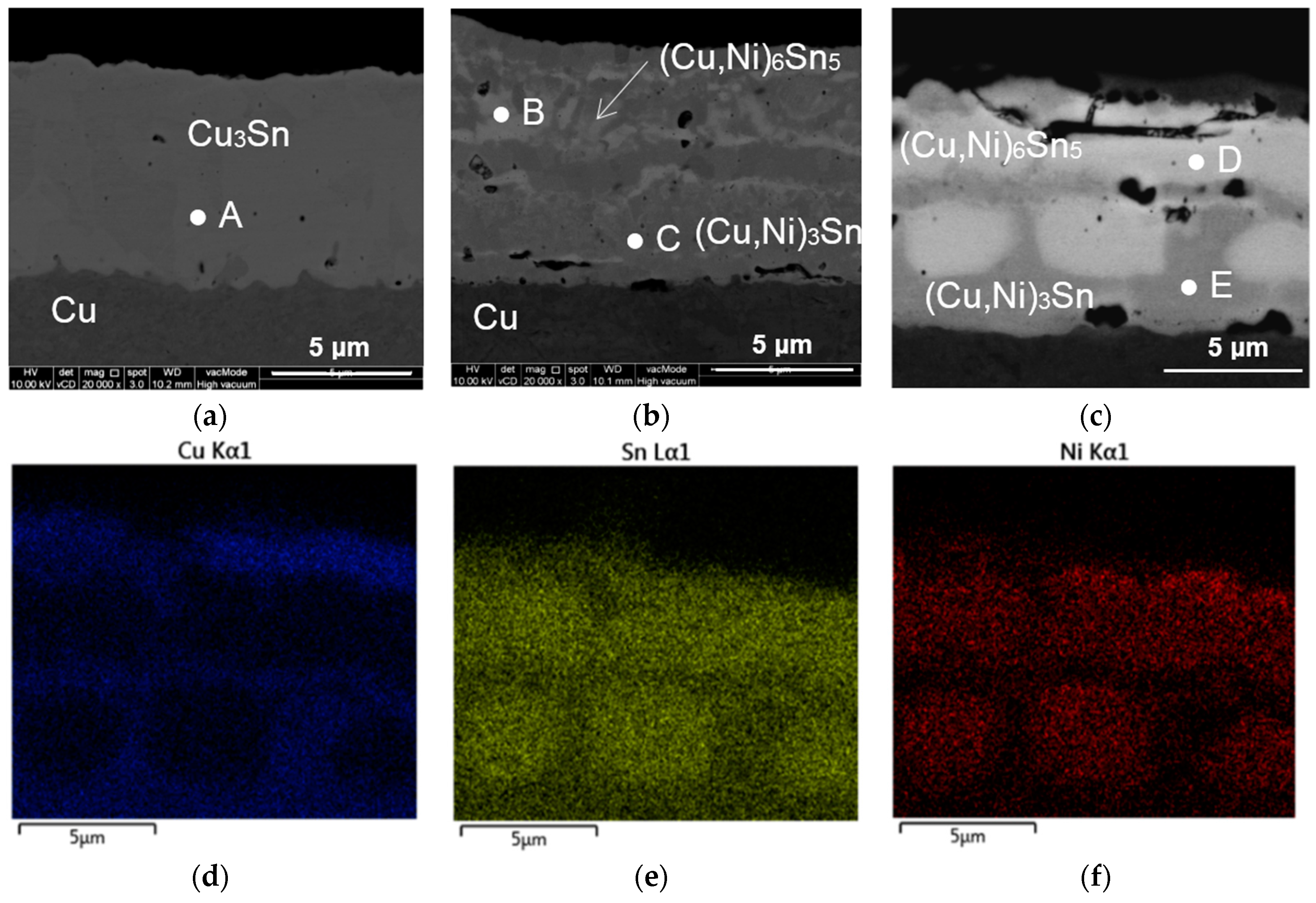
| Spot | Composition (at %) | Ratio | Phase Identified | ||
|---|---|---|---|---|---|
| Cu | Sn | Ni | |||
| A | 76.27 | 23.73 | – | Cu:Sn 3.21:1.00 | Cu3Sn |
| B | 55.27 | 35.12 | 9.61 | (Cu + Ni):Sn 9.28:5.00 | (Cu,Ni)6Sn5 |
| C | 72.35 | 25.78 | 1.87 | (Cu + Ni):Sn 2.88:1.00 | (Cu,Ni)3Sn |
| D | 37.74 | 44.41 | 17.85 | (Cu + Ni):Sn 6.26:5.00 | (Cu,Ni)6Sn5 |
| E | 70.06 | 25.38 | 4.56 | (Cu + Ni):Sn 2.94:1.00 | (Cu,Ni)3Sn |
© 2016 by the authors; licensee MDPI, Basel, Switzerland. This article is an open access article distributed under the terms and conditions of the Creative Commons Attribution (CC-BY) license (http://creativecommons.org/licenses/by/4.0/).
Share and Cite
Chia, P.Y.; Haseeb, A.S.M.A.; Mannan, S.H. Reactions in Electrodeposited Cu/Sn and Cu/Ni/Sn Nanoscale Multilayers for Interconnects. Materials 2016, 9, 430. https://doi.org/10.3390/ma9060430
Chia PY, Haseeb ASMA, Mannan SH. Reactions in Electrodeposited Cu/Sn and Cu/Ni/Sn Nanoscale Multilayers for Interconnects. Materials. 2016; 9(6):430. https://doi.org/10.3390/ma9060430
Chicago/Turabian StyleChia, Pay Ying, A. S. M. A. Haseeb, and Samjid Hassan Mannan. 2016. "Reactions in Electrodeposited Cu/Sn and Cu/Ni/Sn Nanoscale Multilayers for Interconnects" Materials 9, no. 6: 430. https://doi.org/10.3390/ma9060430