
Study of Charge Carrier Transport in GaN Sensors

Abstract
:1. Introduction
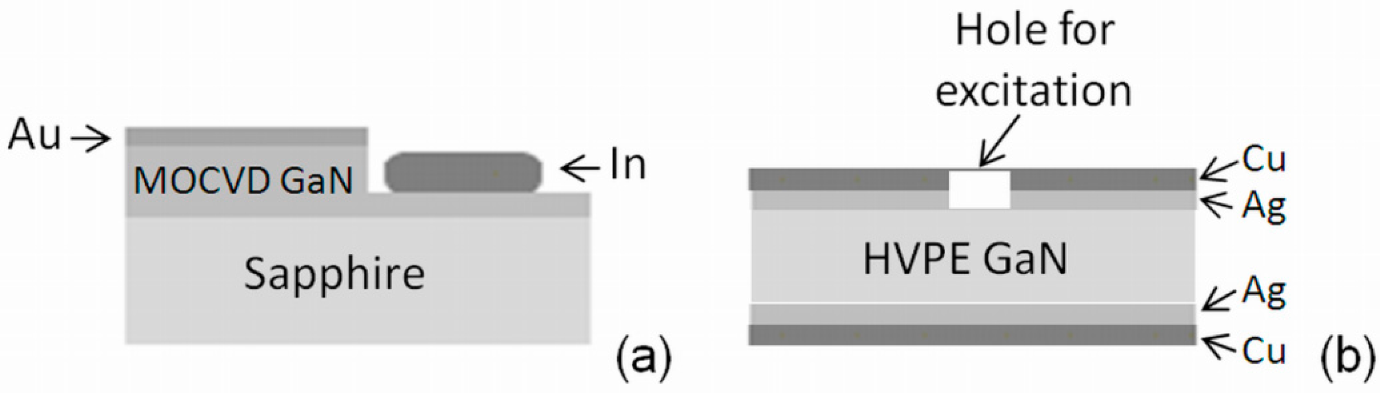
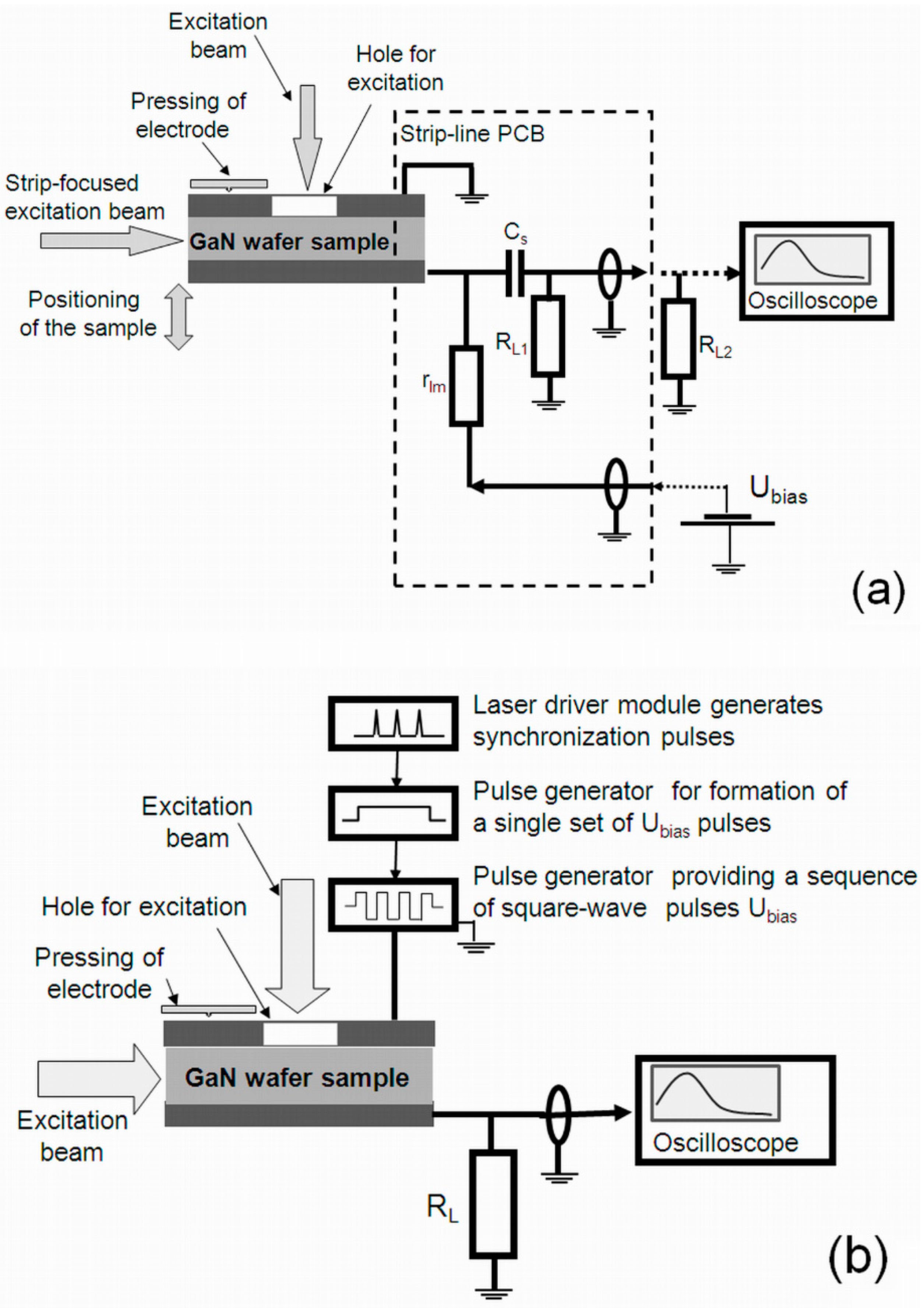
2. Samples and Experimental Regimes
3. Models for Analysis of Current Transients
4. Experimental Results and Discussion
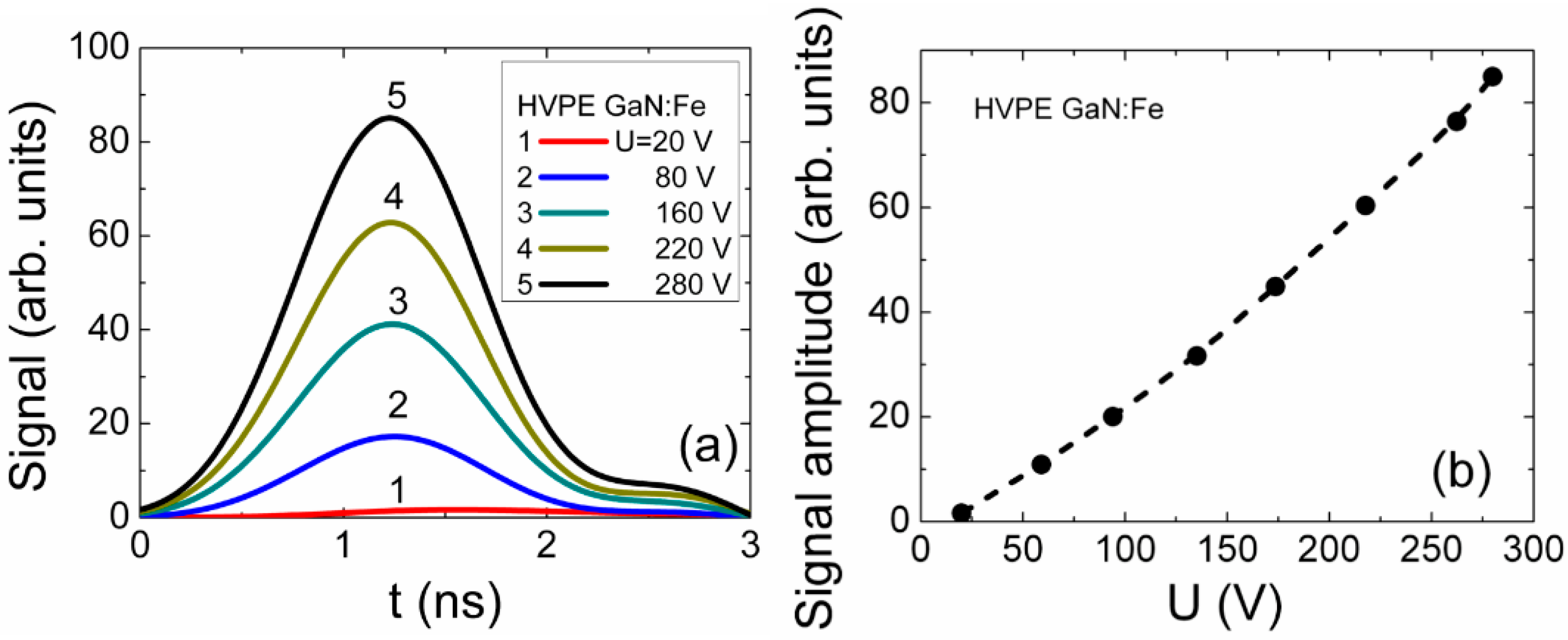
4.1. Recombination Characteristics
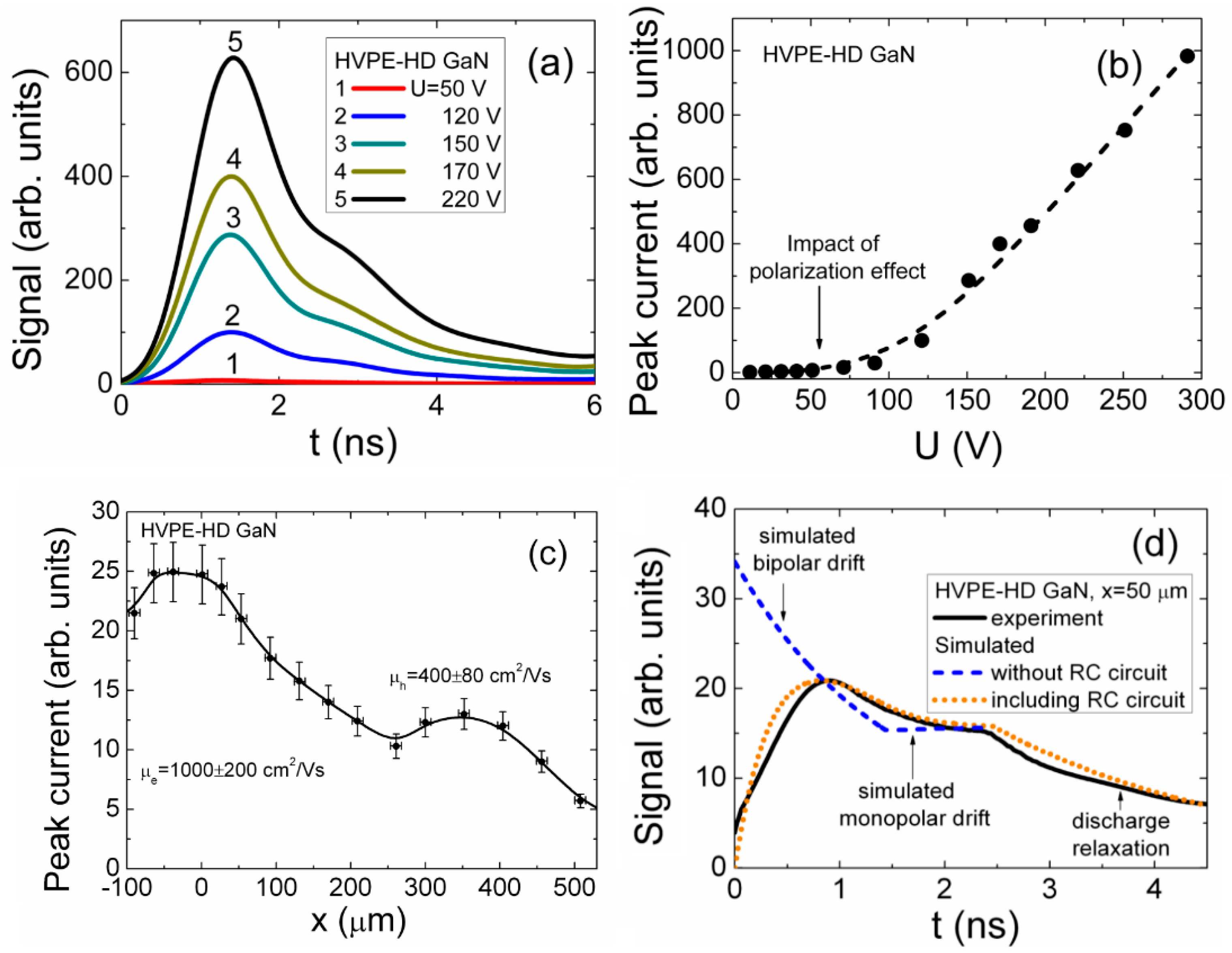
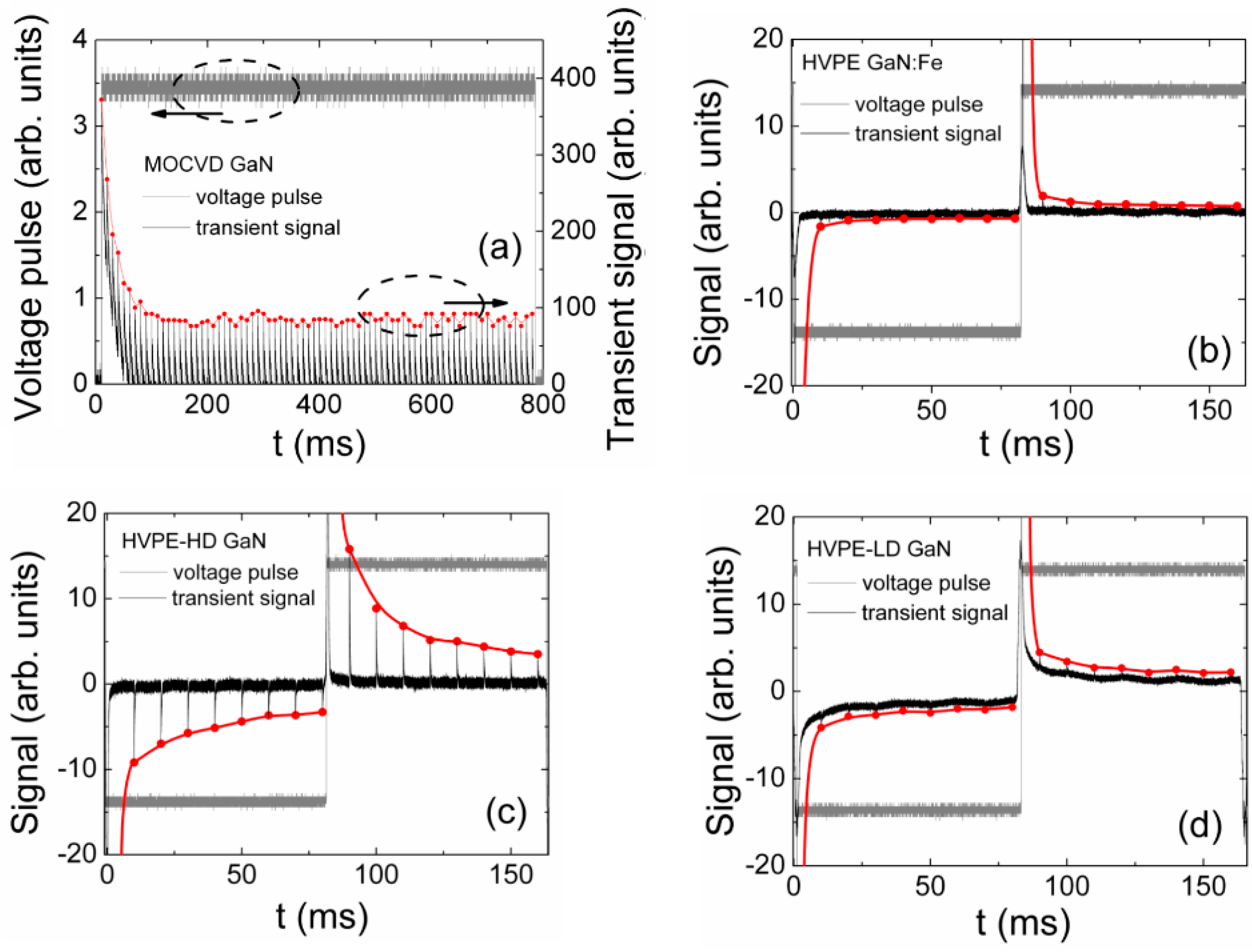
4.2. Profiling of Current Transients in HVPE GaN Sensors
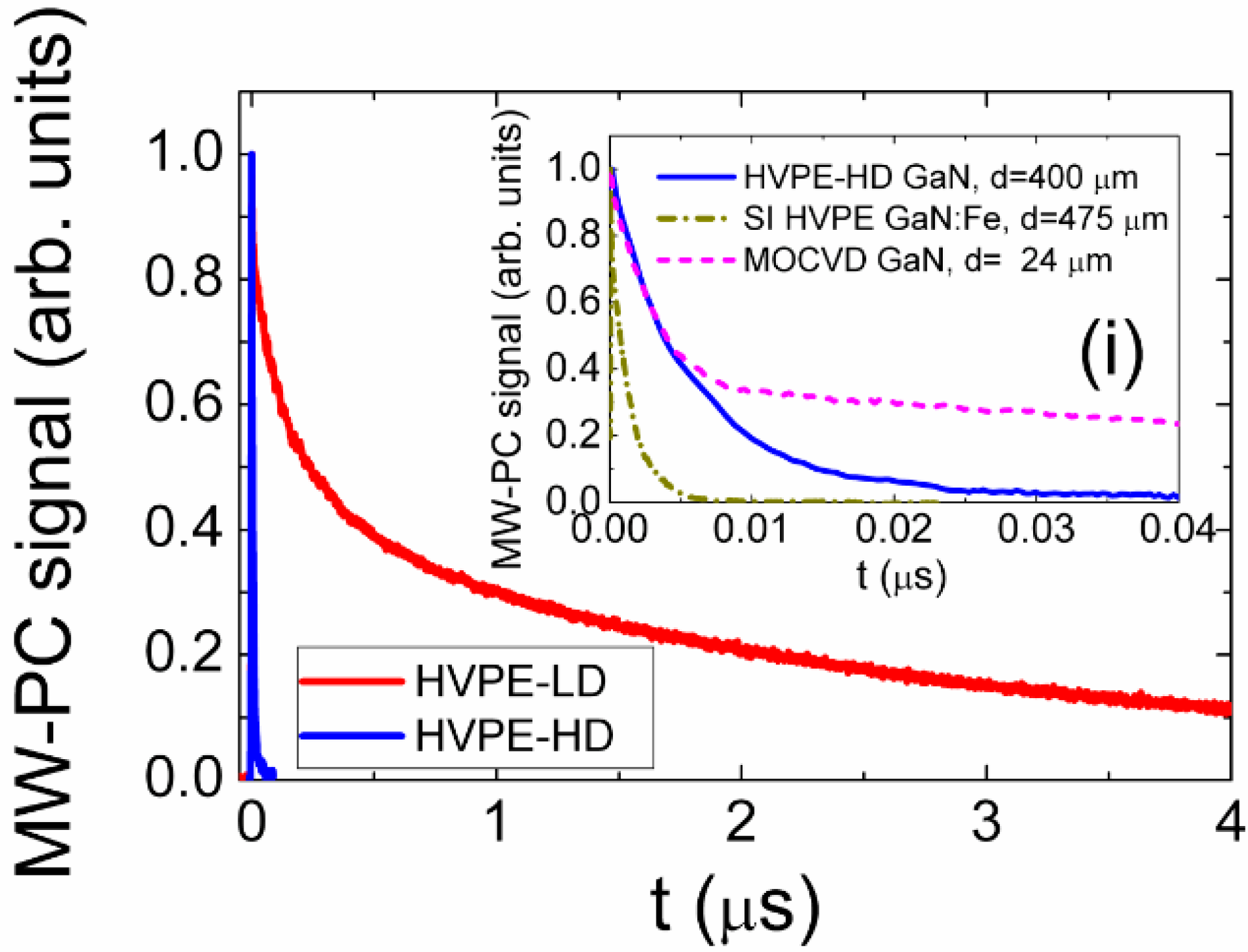
4.3. Current Transients in GaN Materials with Short Carrier Lifetime
4.4. Polarization Effects
5. Summary
Acknowledgments
Author Contributions
Conflicts of Interest
References
- Razeghi, M.; Rogalski, A. Semiconductor ultraviolet detectors. J. Appl. Phys. 1996, 79, 7433–7473. [Google Scholar] [CrossRef]
- Moll, M. Radiation tolerant semiconductor sensors for tracking detectors. Nucl. Instr. Meth. Phys. Res. A 2006, 565, 202–211. [Google Scholar] [CrossRef]
- Pittet, P.; Lu, G.N.; Galvan, J.M.; Loisy, J.Y.; Ismail, A.; Giraud, J.Y.; Balosso, J. Implantable real-time dosimetric probe using GaN as scintillation material. Sens. Actuator A Phys. 2009, 151, 29–34. [Google Scholar] [CrossRef]
- Sellin, P.J.; Vaitkus, J. New materials for radiation hard semiconductor detectors. Nucl. Instr. Meth. Phys. Res. A 2006, 557, 479–489. [Google Scholar] [CrossRef] [Green Version]
- Wang, J.H.; Mulligan, P.; Cao, L.R. Transient current analysis of a GaN radiation detector by TCAD. Nucl. Instr. Meth. Phys. Res. A 2014, 761, 7–12. [Google Scholar] [CrossRef]
- Grant, J.; Bates, R.; Cunningham, W.; Blue, A.; Melone, J.; McEwan, F.; Vaitkus, J.; Gaubas, E.; O’Shea, V. GaN as a radiation hard particle detector. Nucl. Instr. Meth. Phys. Res. A 2007, 576, 60–65. [Google Scholar] [CrossRef]
- Ramo, S. Currents induced by electron motion. Proc. Inst. Radio Eng. 1939, 27, 584–585. [Google Scholar] [CrossRef]
- Shockley, A. Currents to conductors induced by a moving point charge. J. Appl. Phys. 1938, 9, 635–636. [Google Scholar] [CrossRef]
- Resta, R. Macroscopic polarization in crystalline dielectrics: The geometric phase approach. Rev. Mod. Phys. 1994, 66, 899–915. [Google Scholar] [CrossRef]
- Bernardini, F.; Fiorentini, V.; Vanderbilt, D. Polarization-based calculation of the dielectric tensor of polar crystals. Phys. Rev. Lett. 2002, 79, 3958–3961. [Google Scholar] [CrossRef]
- Sumiya, M.; Fuke, S. Review of polarity determination and control in GaN. MRS Internet J. Nitride Semicond. Res. 2004, 9, 1–34. [Google Scholar]
- Aixtron. Available online: http://www.aixtron.com/en/products/technologies (accessed on 14 April 2016).
- Gaubas, E.; Ceponis, T.; Kalesinskas, V.; Pavlov, J.; Vysniauskas, J. Simulations of operation dynamics of different type GaN particle sensors. Sensors 2015, 15, 5429–5473. [Google Scholar] [CrossRef] [PubMed]
- Gaubas, E.; Ceponis, T.; Meskauskaite, D.; Kazuchits, N. Profiling of current transients in capacitor type diamond sensors. Sensors 2015, 15, 13424–13458. [Google Scholar] [CrossRef] [PubMed]
- Gaubas, E.; Ceponis, T.; Kalesinskas, V. Currents induced by injected charge in junction detectors. Sensors 2013, 13, 12295–12328. [Google Scholar] [CrossRef] [PubMed]
- Gaubas, E.; Ceponis, T.; Pavlov, J. Pulsed current signals in capacitor type particle detectors. J. Intrum. 2015, 10, 1–8. [Google Scholar] [CrossRef]
- Morkoc, H. Handbook on Nitride Semiconductors and Devices; Wiley-VCH: Hoboken, NJ, USA, 2008. [Google Scholar]
- Smith, A.R.; Feenstra, R.M.; Greve, D.W.; Shin, M.S.; Skowronski, M.; Neugebauer, J.E.; Northrup, J.E. Reconstructions of GaN(0001) and (0001) surfaces: Ga-rich metallic structures. J. Vac. Sci. Technol. B 1998, 16, 1–17. [Google Scholar] [CrossRef]
- Eller, B.S.; Yang, J.; Nemanich, R.J. Polarization effects of GaN and AlGaN: Polarization bound charge, band bending, and electronic surface states. J. Electron. Mater. 2014, 43, 4560–4568. [Google Scholar] [CrossRef]
- Eller, B.S.; Yang, J.; Nemanich, R.J. Electronic surface and dielectric interface states on GaN and AlGaN. J. Vac. Sci. Technol. A 2013, 31, 1–29. [Google Scholar] [CrossRef]
- Gaubas, E.; Simoen, E.; Vanhellemont, J. Review-Carrier lifetime spectroscopy for defect characterization in semiconductor materials and devices. ECS J. Solid State Sci. Technol. 2016, 5, 3108–3137. [Google Scholar] [CrossRef]
- Gaubas, E.; Uleckas, A.; Grigonis, R.; Sirutkaitis, V.; Vanhellemont, J. Microwave probed photoconductivity spectroscopy of deep levels in Ni doped Ge. Appl. Phys. Lett. 2008, 92, 1–3. [Google Scholar] [CrossRef]
- Gaubas, E.; Ceponis, T.; Jasiunas, A.; Jelmakas, E.; Jursenas, S.; Kadys, A.; Malinauskas, T.; Tekorius, A.; Vitta, P. Study of carrier recombination transient characteristics in MOCVD grown GaN dependent on layer thickness. AIP Adv. 2013, 3, 1–12. [Google Scholar] [CrossRef]
- Phillips, J.C. Stretched exponential relaxation in molecular and electronic glasses. Rep. Prog. Phys. 1996, 59, 1133–1207. [Google Scholar] [CrossRef]
- Phillips, J.C. Slow dynamics in glasses: A comparison between theory and experiment. Phys. Rev. B 2006, 73, 104206. [Google Scholar] [CrossRef]
- Pavlov, J.; Ceponis, T.; Gaubas, E.; Meskauskaite, D.; Reklaitis, I.; Vaitkus, J.; Grigonis, R.; Sirutkaitis, V. Comparative study of deep levels in HVPE and MOCVD GaN by combining O-DLTS and pulsed photo-ionization spectroscopy. J. Instrum. 2015, 10, 1–11. [Google Scholar] [CrossRef]
- Look, D.C.; Reynolds, D.C.; Hemsky, J.W.; Sizelove, J.R.; Jones, R.L.; Molnar, R.J. Defect donor and acceptor in GaN. Phys. Rev. Lett. 1997, 79, 2273–2276. [Google Scholar] [CrossRef]
- Nakamura, S.; Mukai, T.; Senoh, M. In situ monitoring and Hall measurements of GaN grown with GaN buffer layers. J. Appl. Phys. 1992, 71, 5543–5549. [Google Scholar] [CrossRef]
- Chin, V.W.L.; Tansley, T.L.; Osotchan, T. Electron mobilities in gallium, indium, and aluminum nitrides. J. Appl. Phys. 1994, 75, 7365–7372. [Google Scholar] [CrossRef]
- Farahmand, M.; Garetto, C.; Bellotti, E.; Brennan, K.F.; Goano, M.; Ghillino, E.; Ghione, G.; Albrecht, J.D.; Ruden, P.P. Monte Carlo simulation of electron transport in the III-nitride wurtzite phase materials system: Binaries and ternaries. IEEE Trans. Electron Device 2001, 48, 535–542. [Google Scholar] [CrossRef]
- Orton, J.W.; Foxo, C.T. Group III nitride semiconductors for short wavelength light-emitting devices. Rep. Prog. Phys. 1998, 61, 1–75. [Google Scholar] [CrossRef]
- Rubin, M.; Newman, N.; Chan, J.S.; Fu, T.C.; Ross, J.T. P-type gallium nitride by reactive ion-beam molecular beam epitaxy with ion implantation, diffusion, or coevaporation of Mg. Appl. Phys. Lett. 1994, 64, 64–66. [Google Scholar] [CrossRef]
- Hecht, K. Zum Mechanismus des lichtelektrischen Primarstromes in isolierenden Kristallen. Z. Phys. 1932, 77, 235–245. [Google Scholar] [CrossRef]


| GaN Sample | Thickness (μm) | Technology | Device Structure |
|---|---|---|---|
| u-GaN | 24 | MOCVD | Cd and SD |
| SI GaN:Fe | 475 | HVPE | Cd |
| HVPE-LD | 400 | HVPE | Cd |
| HVPE-HD | 400 | HVPE | Cd |
© 2016 by the authors; licensee MDPI, Basel, Switzerland. This article is an open access article distributed under the terms and conditions of the Creative Commons Attribution (CC-BY) license (http://creativecommons.org/licenses/by/4.0/).
Share and Cite
Gaubas, E.; Ceponis, T.; Kuokstis, E.; Meskauskaite, D.; Pavlov, J.; Reklaitis, I. Study of Charge Carrier Transport in GaN Sensors. Materials 2016, 9, 293. https://doi.org/10.3390/ma9040293
Gaubas E, Ceponis T, Kuokstis E, Meskauskaite D, Pavlov J, Reklaitis I. Study of Charge Carrier Transport in GaN Sensors. Materials. 2016; 9(4):293. https://doi.org/10.3390/ma9040293
Chicago/Turabian StyleGaubas, Eugenijus, Tomas Ceponis, Edmundas Kuokstis, Dovile Meskauskaite, Jevgenij Pavlov, and Ignas Reklaitis. 2016. "Study of Charge Carrier Transport in GaN Sensors" Materials 9, no. 4: 293. https://doi.org/10.3390/ma9040293