
Compact Layers of Hybrid Halide Perovskites Fabricated via the Aerosol Deposition Process—Uncoupling Material Synthesis and Layer Formation

 , ,
, , 
Abstract
:
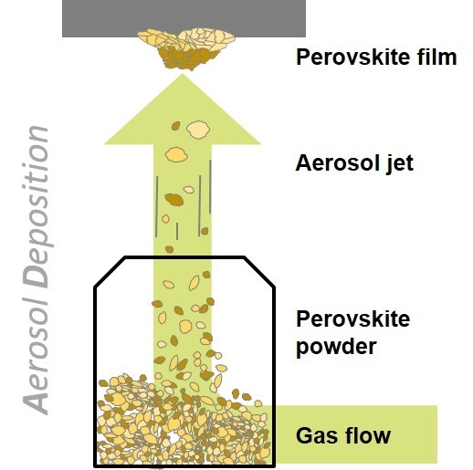
1. Introduction
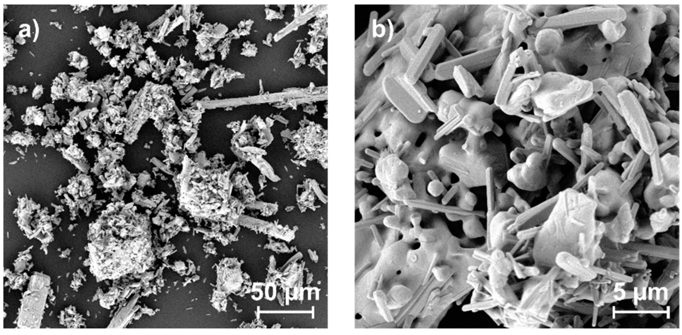
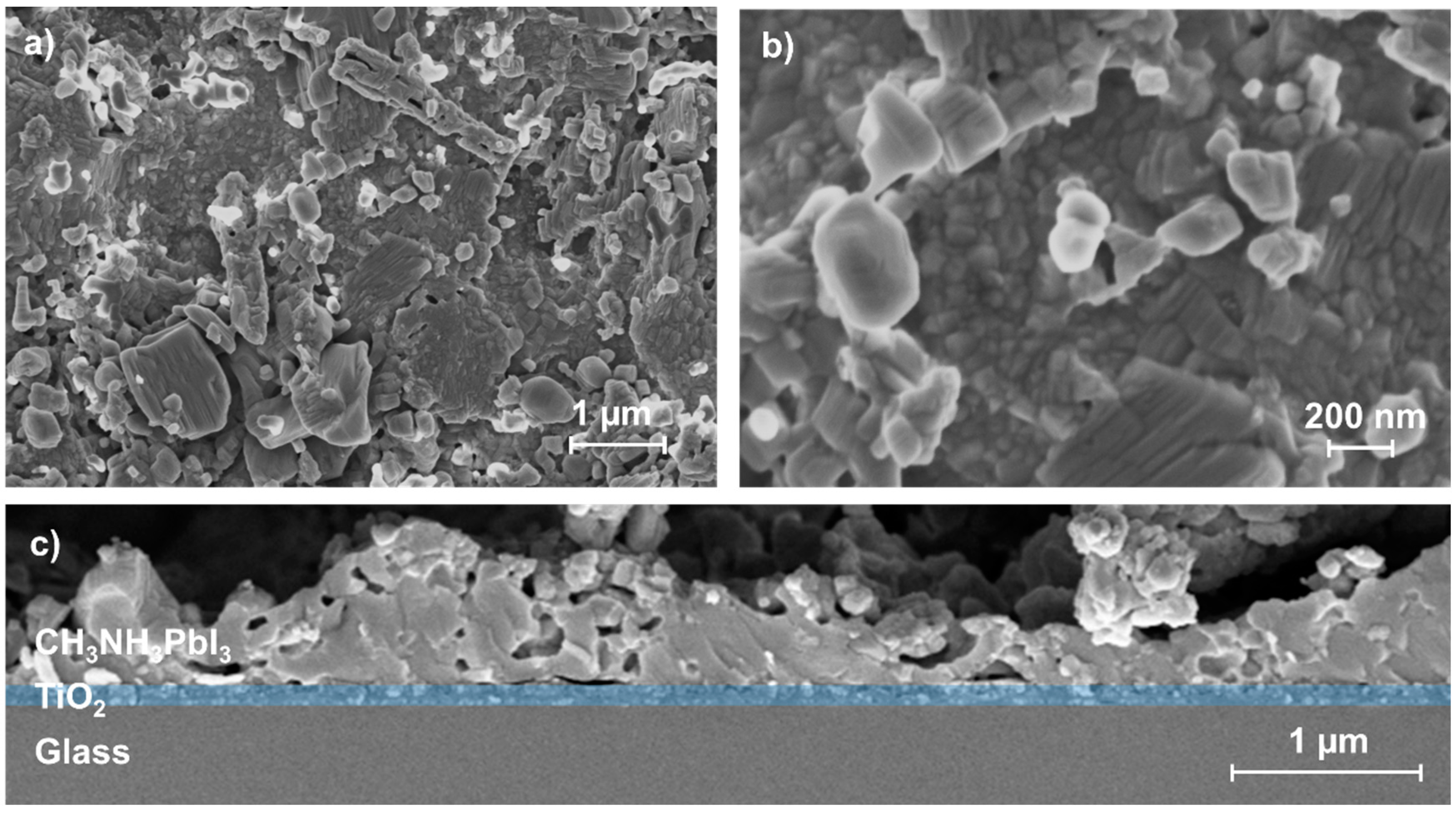
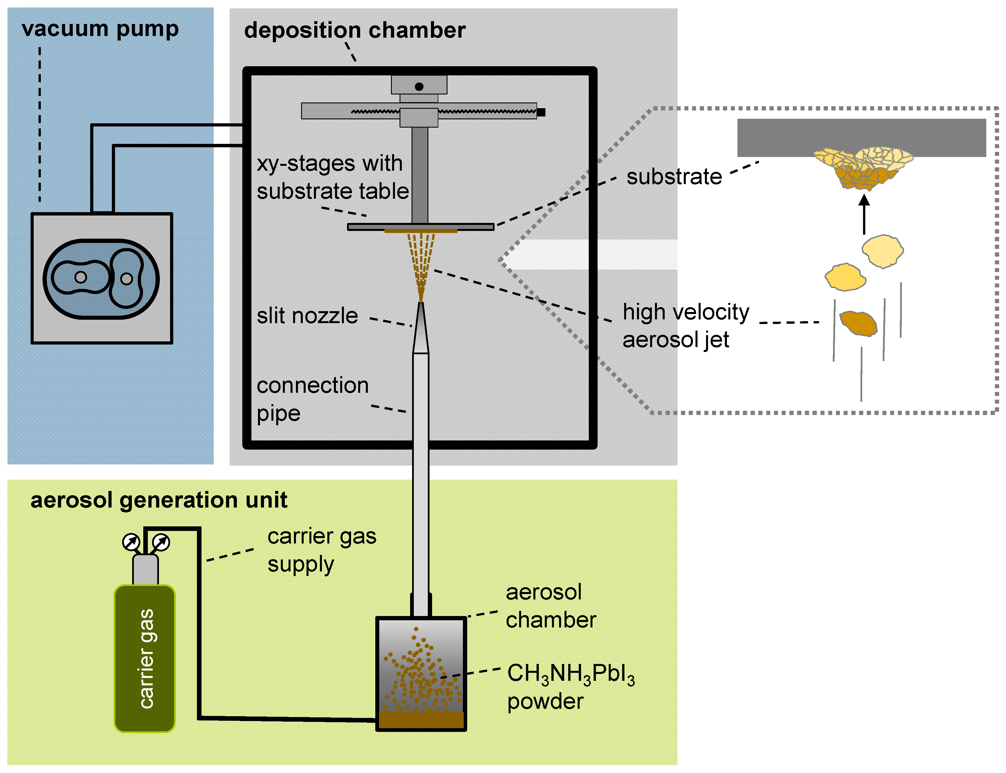
2. Results and Discussion
3. Materials and Methods
Acknowledgments
Author Contributions
Conflicts of Interest
References
- NREL Solar Efficiency Chart. Available online: http://www.nrel.gov/ncpv/images/efficiency_chart.jpg (accessed on 20 February 2015).
- Luo, S.; Daoud, W. Crystal Structure Formation of CH3NH3PbI3-xClx Perovskite. Materials 2016, 9, 123. [Google Scholar] [CrossRef]
- Deschler, F.; Price, M.; Pathak, S.; Klintberg, L.E.; Jarausch, D.D.; Higler, R.; Hüttner, S.; Leijtens, T.; Stranks, S.D.; Snaith, H.J.; et al. High photoluminescence efficiency and optically pumped lasing in solution-processed mixed halide perovskite semiconductors. J. Phys. Chem. Lett. 2014, 5, 1421–1426. [Google Scholar] [CrossRef] [PubMed]
- Zhu, H.; Fu, Y.; Meng, F.; Wu, X.; Gong, Z.; Ding, Q.; Gustafsson, M.V.; Trinh, M.T.; Jin, S.; Zhu, X.Y. Lead halide perovskite nanowire lasers with low lasing thresholds and high quality factors. Nat. Mater. 2015, 14, 636–642. [Google Scholar] [CrossRef] [PubMed]
- Stranks, S.D.; Wood, S.M.; Wojciechowski, K.; Deschler, F.; Saliba, M.; Khandelwal, H.; Patel, J.B.; Elston, S.J.; Herz, L.M.; Johnston, M.B.; et al. Enhanced amplified spontaneous emission in perovskites using a flexible cholesteric liquid crystal reflector. Nano Lett. 2015, 15, 4935–4941. [Google Scholar] [CrossRef] [PubMed]
- Saliba, M.; Wood, S.M.; Patel, J.B.; Nayak, P.K.; Huang, J.; Alexander-Webber, J.A.; Wenger, B.; Stranks, S.D.; Horantner, M.T.; Wang, J.T.; et al. Structured organic-inorganic perovskite toward a distributed feedback laser. Adv. Mater. 2016, 28, 923–929. [Google Scholar] [CrossRef] [PubMed]
- Pathak, S.; Sakai, N.; Wisnivesky Rocca Rivarola, F.; Stranks, S.D.; Liu, J.; Eperon, G.E.; Ducati, C.; Wojciechowski, K.; Griffiths, J.T.; Haghighirad, A.A.; et al. Perovskite Crystals for tunable white light emission. Chem. Mater. 2015, 27, 8066–8075. [Google Scholar] [CrossRef]
- Náfrádi, B.; Náfrádi, G.; Forró, L.; Horváth, E. Methylammonium lead iodide for efficient X-ray energy conversion. J. Phys. Chem. C 2015, 119, 25204–25208. [Google Scholar] [CrossRef]
- Maculan, G.; Sheikh, A.D.; Abdelhady, A.L.; Saidaminov, M.I.; Haque, M.A.; Murali, B.; Alarousu, E.; Mohammed, O.F.; Wu, T.; Bakr, O.M. CH3NH3PbCl3 Single Crystals: Inverse Temperature Crystallization and Visible-Blind UV-Photodetector. J. Phys. Chem. Lett. 2015, 6, 3781–3786. [Google Scholar] [CrossRef] [PubMed]
- Yakunin, S.; Sytnyk, M.; Kriegner, D.; Shrestha, S.; Richter, M.; Matt, G.J.; Azimi, H.; Brabec, C.J.; Stangl, J.; Kovalenko, M.V.; et al. Detection of X-ray photons by solution-processed lead halide perovskites. Nat. Photonics 2015, 9, 444–449. [Google Scholar] [CrossRef]
- Wang, F.; Mei, J.; Wang, Y.; Zhang, L.; Zhao, H.; Zhao, D. Fast photoconductive responses in organometal halide perovskite photodetectors. ACS Appl. Mater. Interfaces 2016, 8, 2840–2846. [Google Scholar] [CrossRef] [PubMed]
- Ramasamy, P.; Lim, D.H.; Kim, B.; Lee, S.H.; Lee, M.S.; Lee, J.S. All-inorganic cesium lead halide perovskite nanocrystals for photodetector applications. Chem. Commun. 2016, 52, 2067–2070. [Google Scholar] [CrossRef] [PubMed]
- Yoo, E.J.; Lyu, M.; Yun, J.H.; Kang, C.J.; Choi, Y.J.; Wang, L. Resistive switching behavior in organic-inorganic hybrid CH3NH3PbI3-xClx perovskite for resistive random access memory devices. Adv. Mater. 2015, 27, 6170–6175. [Google Scholar] [CrossRef] [PubMed]
- Panzer, F.; Baderschneider, S.; Gujar, T.P.; Unger, T.; Bagnich, S.; Jakoby, M.; Bässler, H.; Hüttner, S.; Köhler, J.; Moos, R.; et al. Reversible laser induced amplified spontaneous emission from coexisting tetragonal and orthorhombic phases in hybrid lead halide perovskites. Adv. Opt. Mater. 2016. [Google Scholar] [CrossRef]
- Chin, X.Y.; Cortecchia, D.; Yin, J.; Bruno, A.; Soci, C. Lead iodide perovskite light-emitting field-effect transistor. Nat. Commun. 2015, 6, 7383. [Google Scholar] [CrossRef] [PubMed]
- Stranks, S.D.; Nayak, P.K.; Zhang, W.; Stergiopoulos, T.; Snaith, H.J. Formation of thin films of organic-inorganic perovskites for high-efficiency solar cells. Angew. Chem. Int. Ed. 2015, 54, 3240–3248. [Google Scholar] [CrossRef] [PubMed]
- Ono, L.K.; Leyden, M.R.; Wang, S.; Qi, Y. Organometal halide perovskite thin films and solar cells by vapor deposition. J. Mater. Chem. A 2016. [Google Scholar] [CrossRef]
- Schubert, M.; Exner, J.; Moos, R. Influence of carrier gas composition on the stress of Al2O3 coatings prepared by the aerosol deposition method. Materials 2014, 7, 5633–5642. [Google Scholar] [CrossRef]
- Sahner, K.; Kaspar, M.; Moos, R. Assessment of the novel aerosol deposition method for room temperature preparation of metal oxide gas sensor films. Sens. Actuators B Chem. 2009, 139, 394–399. [Google Scholar] [CrossRef]
- Hanft, D.; Exner, J.; Schubert, M.; Stöcker, T.; Fuierer, P.; Moos, R. An overview of the aerosol deposition method: Process fundamentals and new trends in materials applications. J. Ceram. Sci. Technol. 2015, 6, 147–182. [Google Scholar]
- Exner, J.; Hahn, M.; Schubert, M.; Hanft, D.; Fuierer, P.; Moos, R. Powder requirements for aerosol deposition of alumina films. Adv. Powder Technol. 2015, 26, 1143–1151. [Google Scholar] [CrossRef]
- Exner, J.; Fuierer, P.; Moos, R. Aerosol deposition of (Cu,Ti) substituted bismuth vanadate films. Thin Solid Films 2014, 573, 185–190. [Google Scholar] [CrossRef]
- Akedo, J. Room temperature impact consolidation (RTIC) of fine ceramic powder by aerosol deposition method and applications to microdevices. J. Therm. Spray Technol. 2008, 17, 181–198. [Google Scholar] [CrossRef]
- Yang, S.; Kim, H.; Ahn, S.-H.; Lee, C.S. The effect of the agglomerated microstructure of dry-deposited TiO2 electrodes on the performance of dye-sensitized solar cells. Electrochim. Acta 2015, 166, 117–123. [Google Scholar] [CrossRef]
- Cho, S.H.; Yoon, Y.J. Multi-layer TiO2 films prepared by aerosol deposition method for dye-sensitized solar cells. Thin Solid Films 2013, 547, 91–94. [Google Scholar] [CrossRef]
- Bhachu, D.S.; Scanlon, D.O.; Saban, E.J.; Bronstein, H.; Parkin, I.P.; Carmalt, C.J.; Palgrave, R.G. Scalable route to CH3NH3PbI3 perovskite thin films by aerosol assisted chemical vapour deposition. J. Mater. Chem. A 2015, 3, 9071–9073. [Google Scholar] [CrossRef]
- Barrows, A.T.; Pearson, A.J.; Kwak, C.K.; Dunbar, A.D.F.; Buckley, A.R.; Lidzey, D.G. Efficient planar heterojunction mixed-halide perovskite solar cells deposited via spray-deposition. Energy Environ. Sci. 2014, 7, 2944–2950. [Google Scholar] [CrossRef]
- Chen, S.; Briscoe, J.; Shi, Y.; Chen, K.; Wilson, R.M.; Dunn, S.; Binions, R. A simple, low-cost CVD route to high-quality CH3NH3PbI3 perovskite thin films. Cryst. Eng. Comm. 2015, 17, 7486–7489. [Google Scholar] [CrossRef]
- Ishihara, H.; Sarang, S.; Chen, Y.C.; Lin, O.; Phummirat, P.; Thung, L.; Hernandez, J.; Ghosh, S.; Tung, V. Nature inspiring processing route toward high throughput production of perovskite photovoltaics. J. Mater. Chem. A 2016. [Google Scholar] [CrossRef]
- Lewis, D.J.; O’Brien, P. Ambient pressure aerosol-assisted chemical vapour deposition of (CH3NH3)PbBr3, an inorganic-organic perovskite important in photovoltaics. Chem. Commun. 2014, 50, 6319–6321. [Google Scholar] [CrossRef] [PubMed]
- Leyden, M.R.; Ono, L.K.; Raga, S.R.; Kato, Y.; Wang, S.; Qi, Y. High performance perovskite solar cells by hybrid chemical vapor deposition. J. Mater. Chem. A 2014, 2, 18742–18745. [Google Scholar] [CrossRef]
- Lee, D.W.; Kim, H.J.; Kim, Y.H.; Yun, Y.H.; Nam, S.M. Growth process of α-Al2O3 ceramic films on metal substrates fabricated at room temperature by aerosol deposition. J. Am. Ceram. Soc. 2011, 94, 3131–3138. [Google Scholar] [CrossRef]
- Arnold, M.S.; McGraw, G.J.; Forrest, S.R.; Lunt, R.R. Direct vapor jet printing of three color segment organic light emitting devices for white light illumination. Appl. Phys. Lett. 2008, 92, 053301. [Google Scholar] [CrossRef]
- McGraw, G.J.; Forrest, S.R. Vapor-Phase Microprinting of Multicolor Phosphorescent Organic Light Emitting Device Arrays. Adv. Mater. 2013, 25, 1583–1588. [Google Scholar] [CrossRef] [PubMed]
- Shi, S.W.; Li, Y.F.; Li, X.Y.; Wang, H.Q. Advancements in all-solid-state hybrid solar cells based on organometal halide perovskites. Mater. Horiz. 2015, 2, 378–405. [Google Scholar] [CrossRef]
- Galisteo-Lopez, J.F.; Anaya, M.; Calvo, M.E.; Miguez, H. Environmental effects on the photophysics of organic-inorganic halide perovskites. J. Phys. Chem. Lett. 2015, 6, 2200–2205. [Google Scholar] [CrossRef] [PubMed]
- Stranks, S.D.; Eperon, G.E.; Grancini, G.; Menelaou, C.; Alcocer, M.J.; Leijtens, T.; Herz, L.M.; Petrozza, A.; Snaith, H.J. Electron-hole diffusion lengths exceeding 1 micrometer in an organometal trihalide perovskite absorber. Science 2013, 342, 341–344. [Google Scholar] [CrossRef] [PubMed]
- Gujar, T.P.; Thelakkat, M. Highly reproducible and efficient perovskite solar cells with extraordinary stability from robust CH3NH3PbI3: Towards large-area devices. Energy Technol. 2016, 4, 449–457. [Google Scholar] [CrossRef]
- Liu, M.; Johnston, M.B.; Snaith, H.J. Efficient planar heterojunction perovskite solar cells by vapour deposition. Nature 2013, 501, 395–398. [Google Scholar] [CrossRef] [PubMed]
- Chen, Q.; Zhou, H.; Hong, Z.; Luo, S.; Duan, H.S.; Wang, H.H.; Liu, Y.; Li, G.; Yang, Y. Planar heterojunction perovskite solar cells via vapor-assisted solution process. J. Am. Chem. Soc. 2014, 136, 622–625. [Google Scholar] [CrossRef] [PubMed]
- Bellet, D.; Bellet-Amalric, E. Physical Characterisation of Photovoltaic Materials. In Solar Cell Materials; John Wiley & Sons: New York, NY, USA, 2014; pp. 35–63. [Google Scholar]
- Exner, J.; Fuierer, P.; Moos, R. Aerosol codeposition of ceramics: Mixtures of Bi2O3-TiO2 and Bi2O3-V2O5. J. Am. Ceram. Soc. 2014, 98, 717–723. [Google Scholar] [CrossRef]
- Park, J.H.; Akedo, J.; Nakada, M. Surface plasmon resonance in novel nanocomposite gold/lead zirconate titanate films prepared by aerosol deposition method. Jpn. J. Appl. Phys. 2006, 45, 7512–7515. [Google Scholar] [CrossRef]
- Ryu, J.; Hahn, B.D.; Choi, J.J.; Yoon, W.H.; Lee, B.K.; Choi, J.H.; Park, D.S. Porous photocatalytic TiO2 thin films by aerosol deposition. J. Am. Ceram. Soc. 2010, 93, 55–58. [Google Scholar] [CrossRef]


© 2016 by the authors; licensee MDPI, Basel, Switzerland. This article is an open access article distributed under the terms and conditions of the Creative Commons by Attribution (CC-BY) license (http://creativecommons.org/licenses/by/4.0/).
Share and Cite
Panzer, F.; Hanft, D.; Gujar, T.P.; Kahle, F.-J.; Thelakkat, M.; Köhler, A.; Moos, R. Compact Layers of Hybrid Halide Perovskites Fabricated via the Aerosol Deposition Process—Uncoupling Material Synthesis and Layer Formation. Materials 2016, 9, 277. https://doi.org/10.3390/ma9040277
Panzer F, Hanft D, Gujar TP, Kahle F-J, Thelakkat M, Köhler A, Moos R. Compact Layers of Hybrid Halide Perovskites Fabricated via the Aerosol Deposition Process—Uncoupling Material Synthesis and Layer Formation. Materials. 2016; 9(4):277. https://doi.org/10.3390/ma9040277
Chicago/Turabian StylePanzer, Fabian, Dominik Hanft, Tanaji P. Gujar, Frank-Julian Kahle, Mukundan Thelakkat, Anna Köhler, and Ralf Moos. 2016. "Compact Layers of Hybrid Halide Perovskites Fabricated via the Aerosol Deposition Process—Uncoupling Material Synthesis and Layer Formation" Materials 9, no. 4: 277. https://doi.org/10.3390/ma9040277
APA StylePanzer, F., Hanft, D., Gujar, T. P., Kahle, F.-J., Thelakkat, M., Köhler, A., & Moos, R. (2016). Compact Layers of Hybrid Halide Perovskites Fabricated via the Aerosol Deposition Process—Uncoupling Material Synthesis and Layer Formation. Materials, 9(4), 277. https://doi.org/10.3390/ma9040277