
Crystal Quality and Light Output Power of GaN-Based LEDs Grown on Concave Patterned Sapphire Substrate

Abstract
:1. Introduction
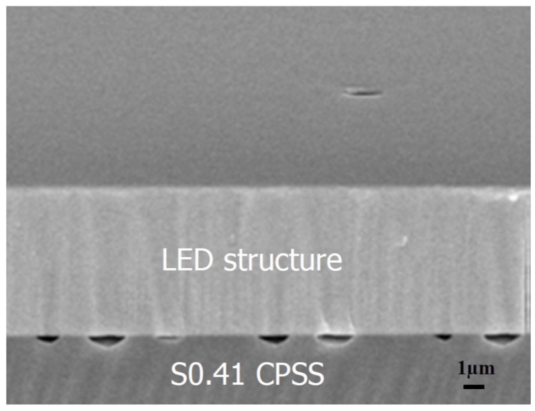
2. Experimental
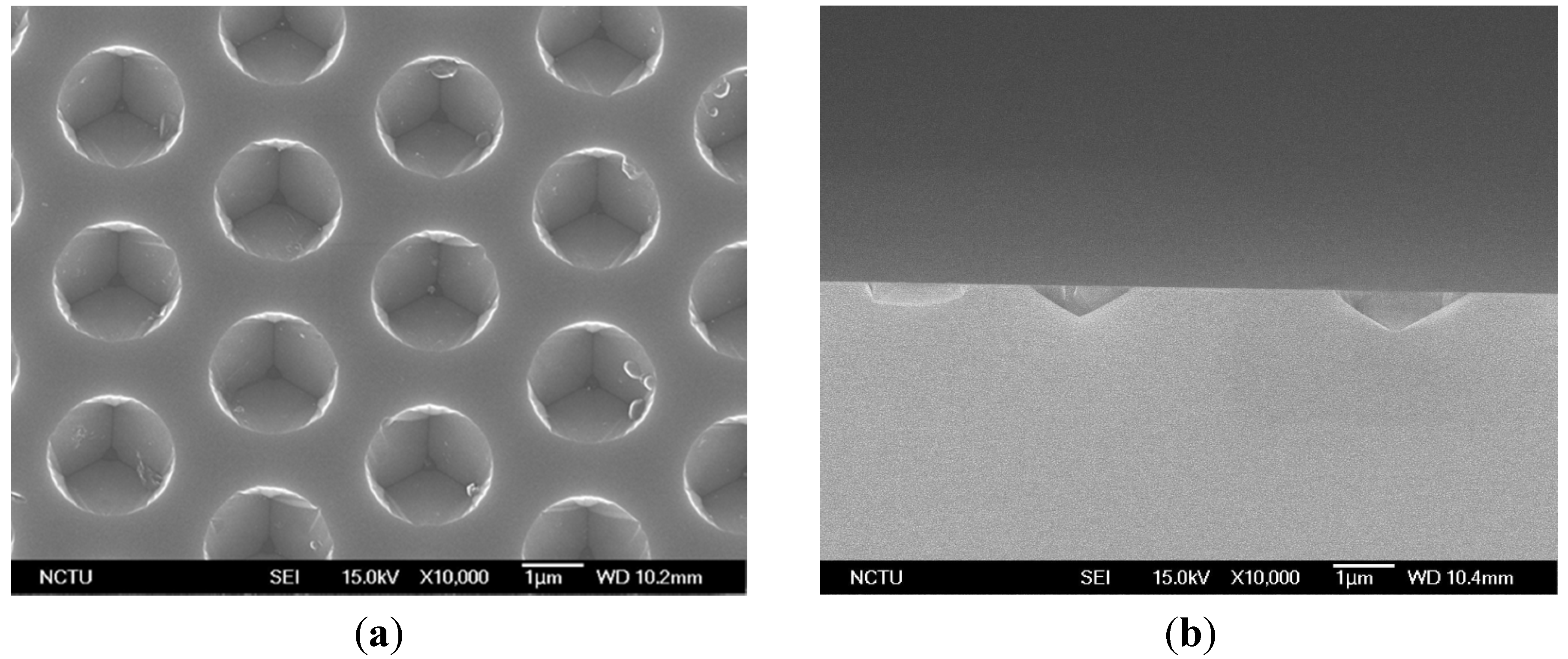

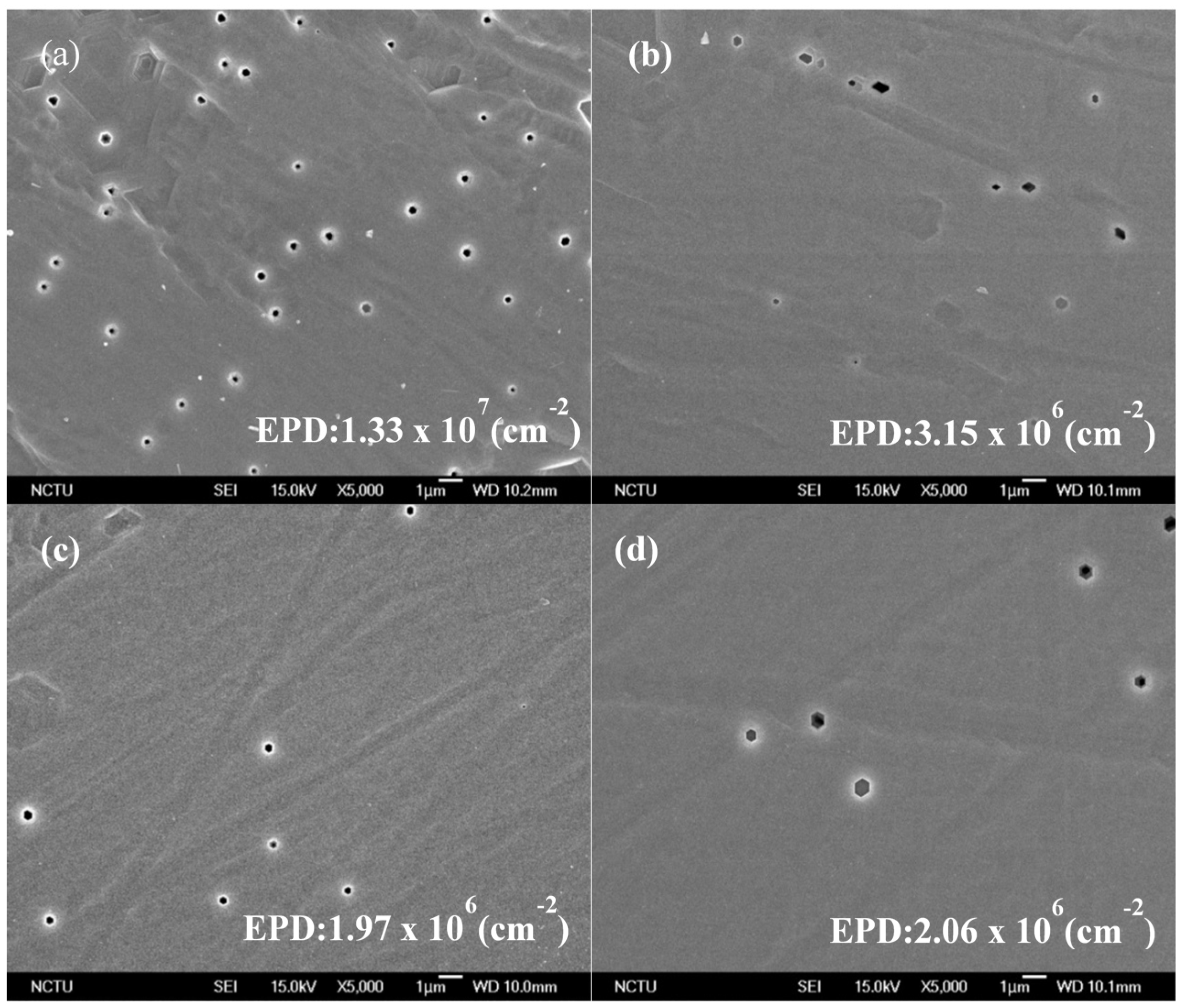
| Sample | Pattern size-Diameter/Spacing (µm) | Percentage of c-plane (%) |
|---|---|---|
| S0.41 | 2.59/0.41 | 32.40 |
| S0.60 | 2.40/0.60 | 41.96 |
| S0.87 | 2.13/0.87 | 54.28 |
| S3.00(FLAT-GaN) | 0.00/3.00 | 100 |
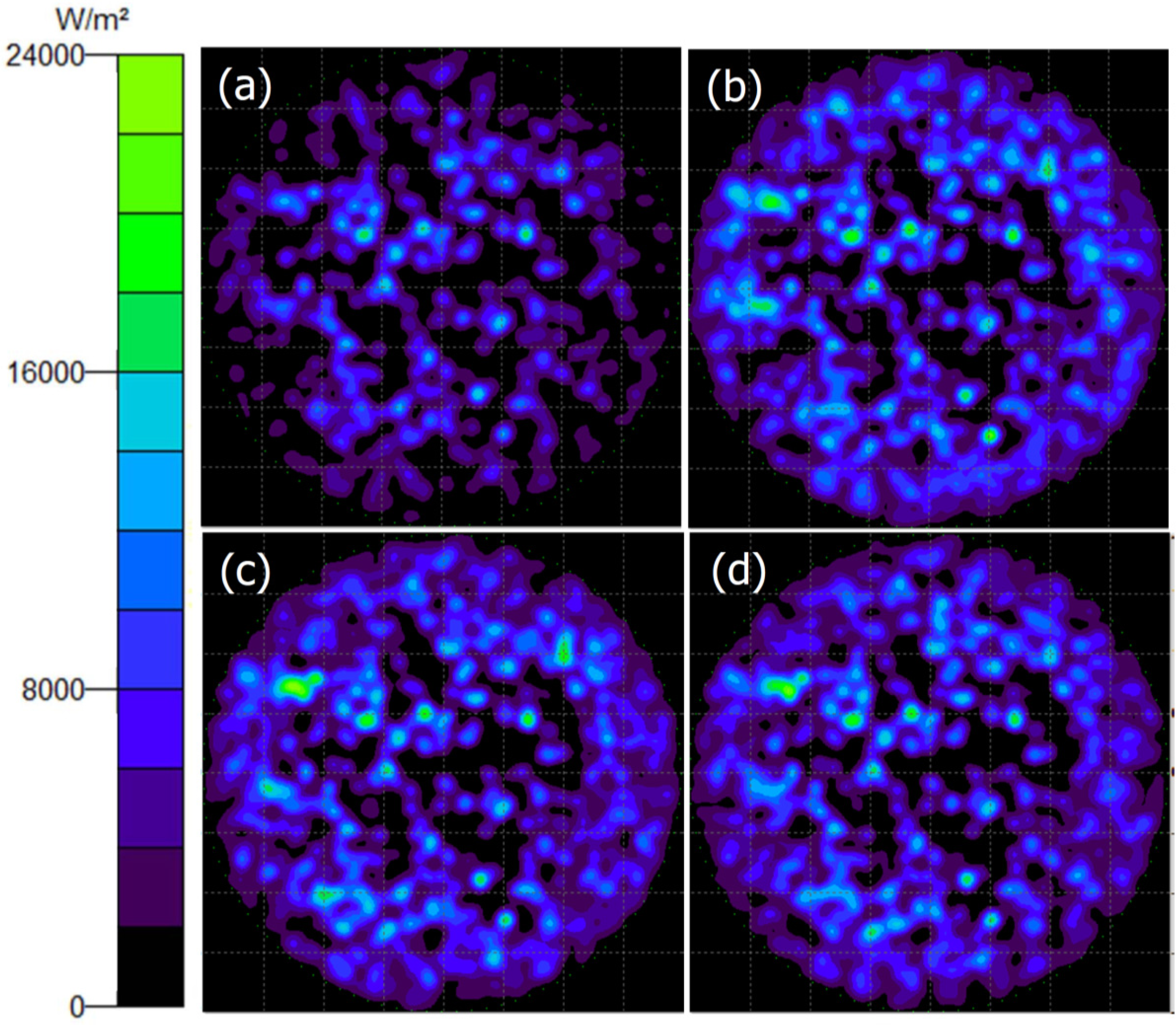
3. Results and Discussion
| FWHM of XRCs (arcsec) | Forward Voltages (V) | LOP (mW) | Simulation of LEE (%) | ||
|---|---|---|---|---|---|
| (002) | (102) | @ 20 mA | @ 20 mA | ||
| S0.41-GaN | 340.2 | 471.2 | 2.79 | 140.7 | 16.59 |
| S0.60-GaN | 336.6 | 442.8 | 2.79 | 115.5 | 16.07 |
| S0.87-GaN | 364.0 | 460.4 | 2.80 | 99.9 | 15.23 |
| S3.00-GaN | 369.7 | 502.6 | – | – | 9.19 |


4. Conclusions
Acknowledgments
Author Contributions
Conflicts of Interest
References
- Sakai, A.; Sunakawa, H.; Usui, A. Defect structure in selectively grown GaN films with low threading dislocation density. Appl. Phys. Lett. 1997, 71, 2259–2261. [Google Scholar] [CrossRef]
- Boroditsky, M.; Yablonovitch, E. Light-emitting diode extraction efficiency. Proc. SPIE 1997, 3002, 119–122. [Google Scholar]
- Linthicum, K.; Gehrke, T.; Thomson, D.; Carlson, E.; Rajagopal, P.; Smith, T.; Batchelor, D.; Davis, R. Pendeoepitaxy of gallium nitride thin films. Appl. Phys. Lett. 1999, 75, 196–198. [Google Scholar] [CrossRef]
- Chang, S.J.; Chang, C.S.; Su, Y.K.; Chuang, R.W.; Lai, W.C.; Kuo, C.H.; Hsu, Y.P.; Lin, Y.C.; Shei, S.C.; Lo, H.M.; et al. Nitride-based LEDs with an SPS tunneling contact layer and an ITO transparent contact. IEEE Photon. Technol. Lett. 2004, 16, 1002–1004. [Google Scholar] [CrossRef]
- Peng, W.C.; Wu, Y.S. Enhanced performance of an InGaN–GaN light-emitting diode by roughening the undoped-GaN surface and applying a mirror coating to the sapphire substrate. Appl. Phys. Lett. 2006, 88. [Google Scholar] [CrossRef]
- Han, D.S.; Kim, J.Y.; Na, S.I.; Kim, S.H.; Lee, K.D.; Kim, B.; Park, S.J. Improvement of light extraction efficiency of flip-chip light-emitting diode by texturing the bottom side-surface of sapphire substrate. IEEE Photon. Technol. Lett. 2006, 18, 1406–1408. [Google Scholar] [CrossRef]
- Lee, C.E.; Lee, Y.J.; Kuo, H.C.; Tsai, M.R.; Cheng, B.S.; Lu, T.C.; Wang, S.C.; Kuo, C.T. Enhancement of flip-chip light-emitting diodes with omni-directional reflector and textured micropillar arrays. IEEE Photon. Technol. Lett. 2007, 19, 1200–1202. [Google Scholar] [CrossRef]
- Huang, H.W.; Lin, C.H.; Yu, C.C.; Lee, B.D.; Chiu, C.H.; Lai, C.F.; Kuo, H.C.; Leung, K.M.; Lu, T.C.; Wang, S.C. Enhanced light output from a nitride-based power chip of green light-emitting diodes with nano-rough surface using nanoimprint lithography. Nanotechnology 2008, 19. [Google Scholar] [CrossRef]
- Tadatomo, K.; Okagawa, H.; Ohuchi, Y.; Tsunekawa, T.; Imada, Y.; Kato, M.; Taguchi, T. High output power ingan ultraviolet light-emitting diodes fabricated on patterned substrates using metalorganic vapor phase epitaxy. J. Jpn. Appl. Phys. 2001, 40, L583–L585. [Google Scholar] [CrossRef]
- Wuu, D.S.; Wang, W.K.; Shih, W.C.; Horng, R.H.; Lee, C.E.; Lin, W.Y.; Fang, J.S. Enhanced output power of near-ultraviolet InGaN-GaN LEDs grown on patterned sapphire substrates. IEEE Photon. Technol. Lett. 2005, 17, 288–290. [Google Scholar] [CrossRef]
- Feng, Z.H.; Lau, K.M. Enhanced luminescence from GaN-based blue LEDs grown on grooved sapphire substrates. IEEE Photon. Technol. Lett. 2005, 17, 1812–1814. [Google Scholar] [CrossRef]
- Lee, Y.J.; Hwang, J.M.; Hsu, T.C.; Hsieh, M.H.; Jou, M.J.; Lee, B.J.; Lu, T.C.; Kuo, H.C.; Wang, S.C. Enhancing the output power of GaN-based LEDs grown on wet-etched patterned sapphire substrates. IEEE Photon. Technol. Lett. 2006, 18, 1152–1154. [Google Scholar] [CrossRef]
- Yamada, M.; Mitani, T.; Narukawa, Y.; Shioji, S.; Niki, I.; Sonobe, S.; Deguchi, K.; Sano, M.; Mukai, T. InGaN-based near-ultraviolet and blue-light-emitting diodes with high external quantum efficiency using a patterned sapphire substrate and a mesh electrode. J. Jpn. Appl. Phys. 2002, 41, L1431–L1433. [Google Scholar] [CrossRef]
- Pan, C.; Hsieh, C.; Lin, C.; Chyi, J. Light output improvement of InGaN ultraviolet light-emitting diodes by using wet-etched stripe-patterned sapphire substrates. J. Appl. Phys. 2007, 102. [Google Scholar] [CrossRef]
- Lee, J.H.; Oh, J.T.; Park, J.S.; Kim, J.W.; Kim, Y.C.; Lee, J.W.; Cho, H.K. Improvement of luminous intensity of InGaN light emitting diodes grown on hemispherical patterned sapphire. Phys. Stat. Sol. 2006, 3, 2169–2173. [Google Scholar] [CrossRef]
- Cheng, J.H.; Wu, Y.C.S.; Liao, W.C.; Lin, B.W. Improved crystal quality and performance of GaN-based light-emitting diodes by decreasing the slanted angle of patterned sapphire. Appl. Phys. Lett. 2010, 96. [Google Scholar] [CrossRef]
- Wang, W.; Wuu, D.; Shih, W.; Fang, J.; Lee, C.; Lin, W.; Han, P.; Horng, R.; Hsu, T.; Huo, T.; et al. Near-ultraviolet InGaN/GaN light-emitting diodes grown on patterned sapphire substrates. Jpn. J. Appl. Phys. 2005, 44, 2512–2515. [Google Scholar] [CrossRef]
- Chen, C.C.; Hsiao, F.C.; Lin, B.W.; Hsu, W.; Wu, Y.S. Evolution of bottom c-Plane on wet-etched patterned sapphire substrate. ECS J. Solid State Sci. Technol. 2013, 2, R169–R171. [Google Scholar] [CrossRef]
- Lee, T.X.; Lin, C.Y.; Ma, S.H.; Sun, C.C. Analysis of position-dependent light extraction of GaN-based LEDs. Opt. Express 2005, 13, 4175–4179. [Google Scholar] [CrossRef] [PubMed]
© 2015 by the authors; licensee MDPI, Basel, Switzerland. This article is an open access article distributed under the terms and conditions of the Creative Commons Attribution license (http://creativecommons.org/licenses/by/4.0/).
Share and Cite
Wu, Y.S.; Isabel, A.P.S.; Zheng, J.-H.; Lin, B.-W.; Li, J.-H.; Lin, C.-C. Crystal Quality and Light Output Power of GaN-Based LEDs Grown on Concave Patterned Sapphire Substrate. Materials 2015, 8, 1993-1999. https://doi.org/10.3390/ma8041993
Wu YS, Isabel APS, Zheng J-H, Lin B-W, Li J-H, Lin C-C. Crystal Quality and Light Output Power of GaN-Based LEDs Grown on Concave Patterned Sapphire Substrate. Materials. 2015; 8(4):1993-1999. https://doi.org/10.3390/ma8041993
Chicago/Turabian StyleWu, YewChung Sermon, A. Panimaya Selvi Isabel, Jian-Hsuan Zheng, Bo-Wen Lin, Jhen-Hong Li, and Chia-Chen Lin. 2015. "Crystal Quality and Light Output Power of GaN-Based LEDs Grown on Concave Patterned Sapphire Substrate" Materials 8, no. 4: 1993-1999. https://doi.org/10.3390/ma8041993