Films of Carbon Nanomaterials for Transparent Conductors

Abstract
:1. Introduction
2. Carbon Nanotube (CNT) Films
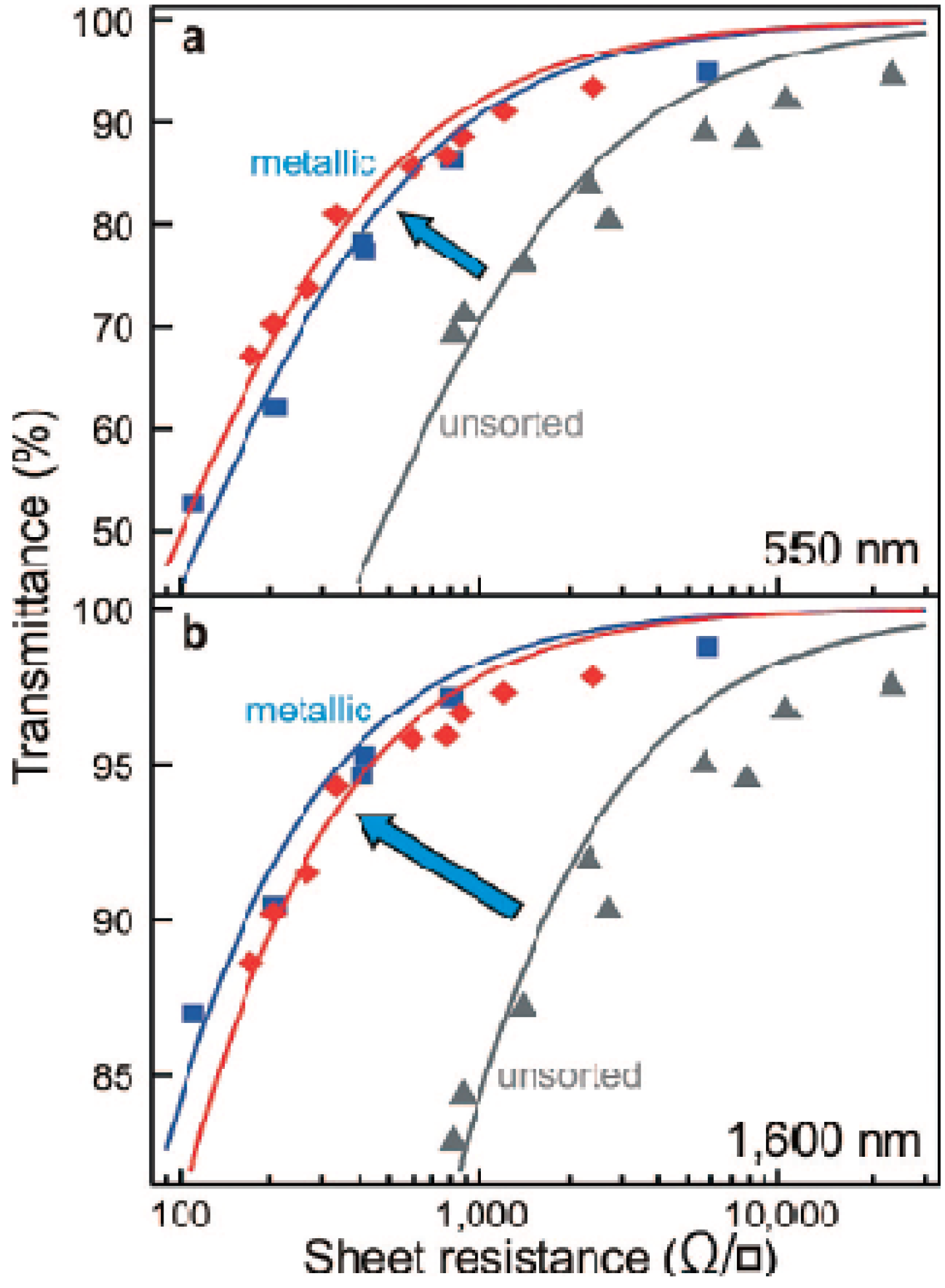
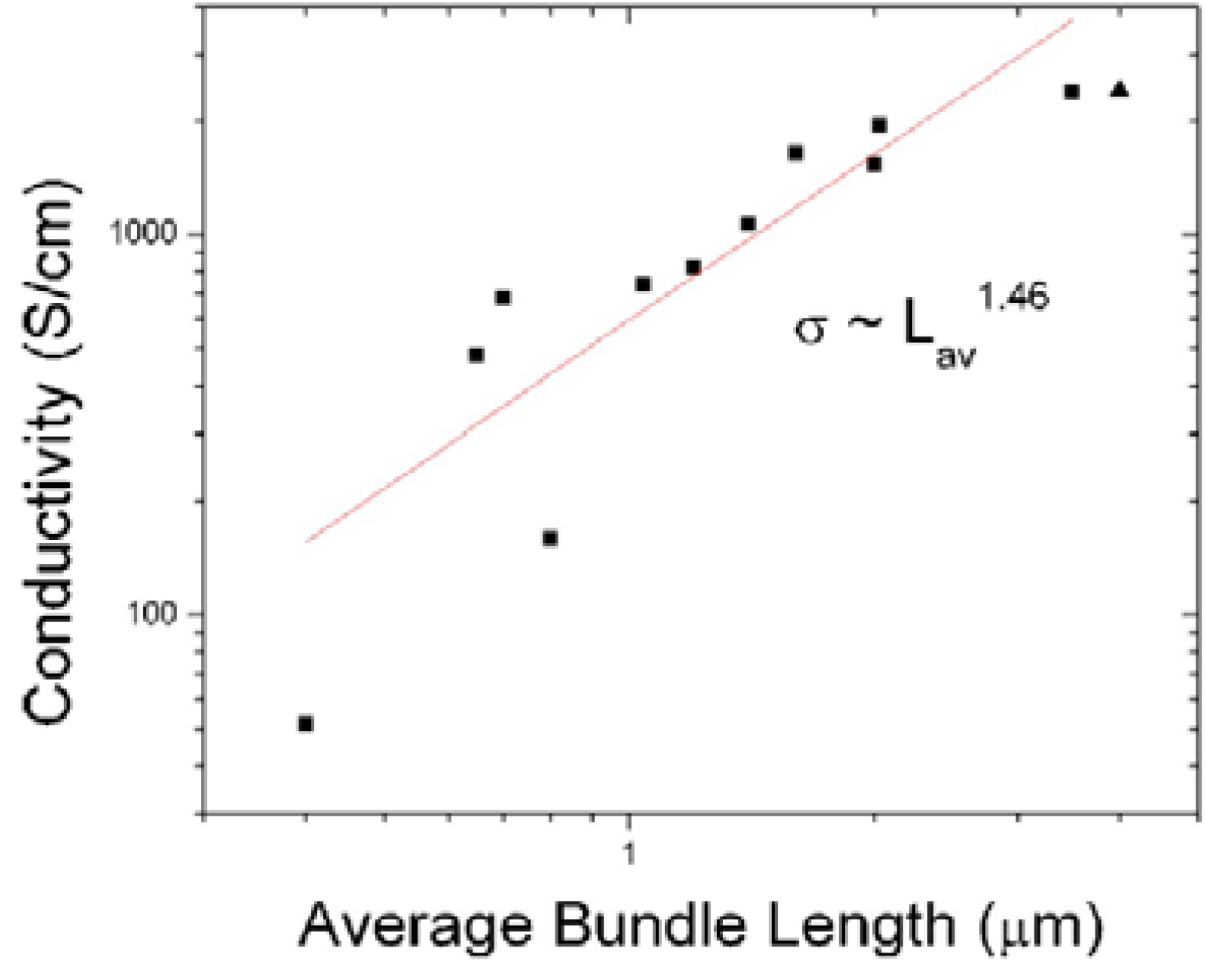
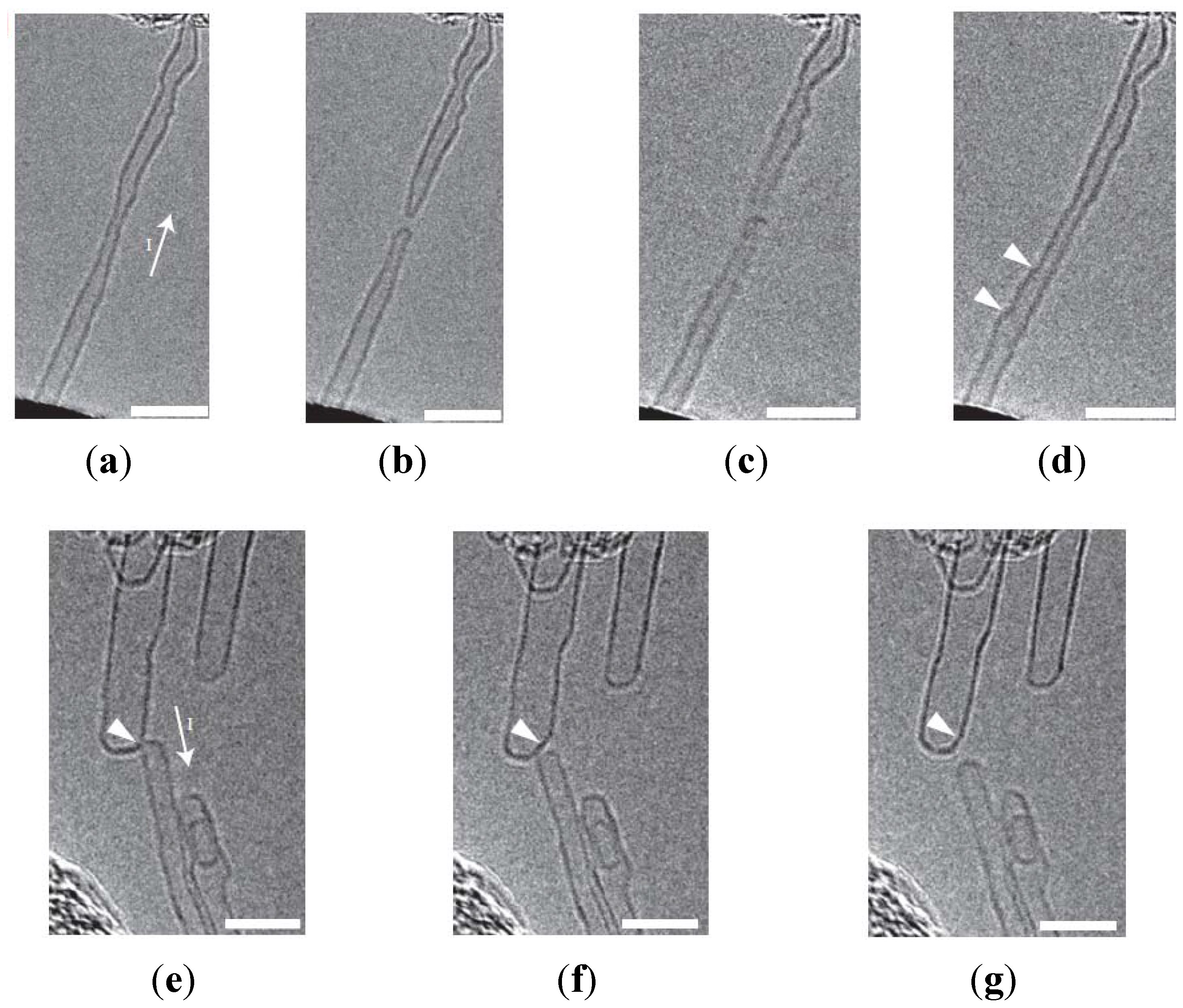
2.1. Properties of Carbon Nanotube (CNT) Thin Films
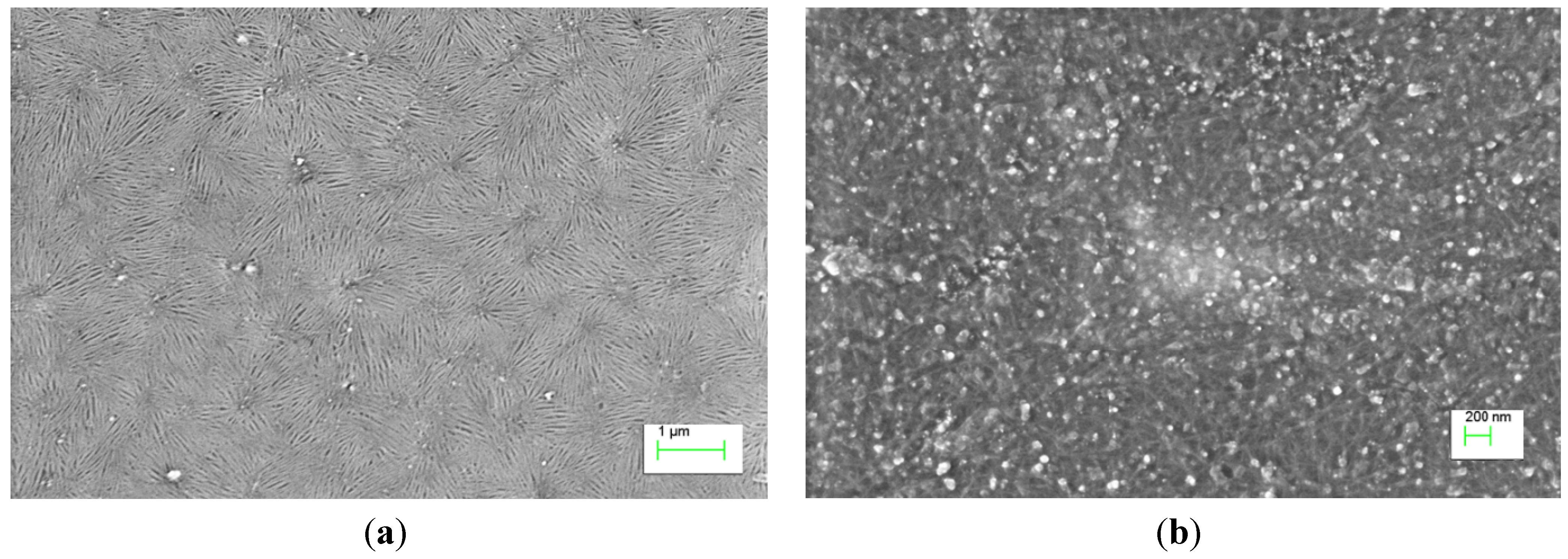
2.2. Carbon Nanotube (CNT) Film Assembly
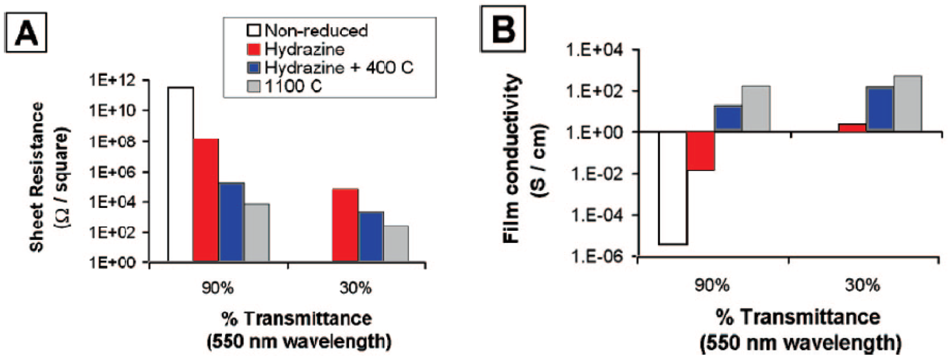
2.3. Post Treatment

3. Graphene Films
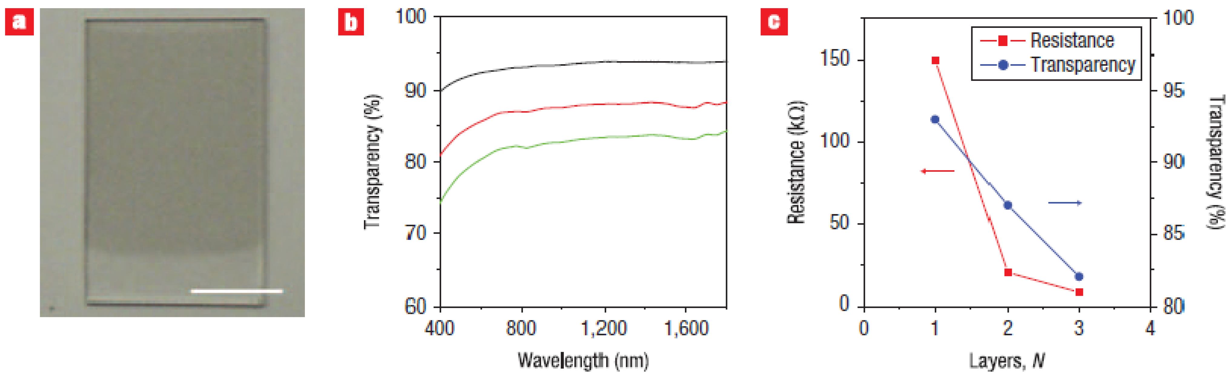
3.1. Synthesis and Assembly of Graphene Films
3.1.1. Solution Processed Films


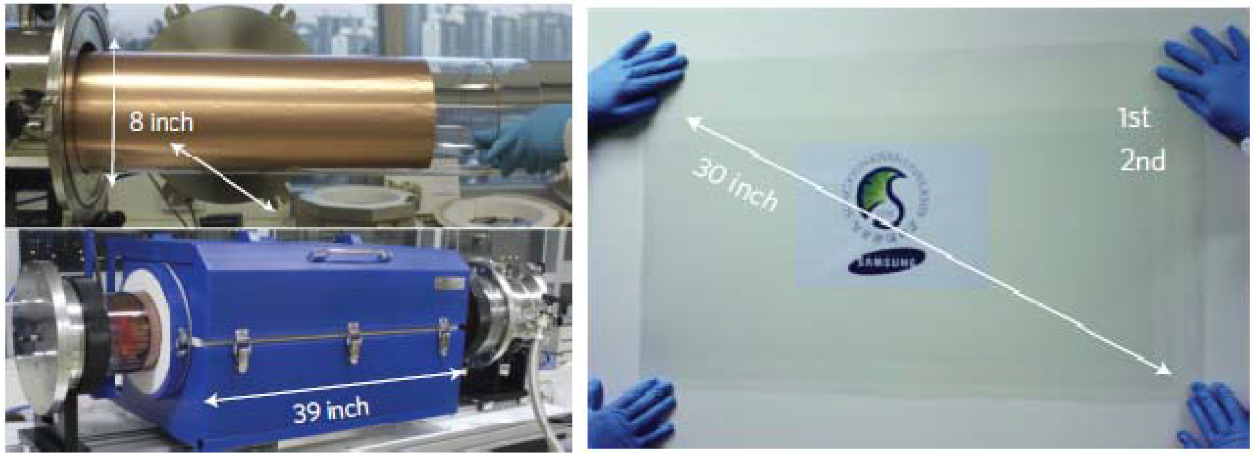
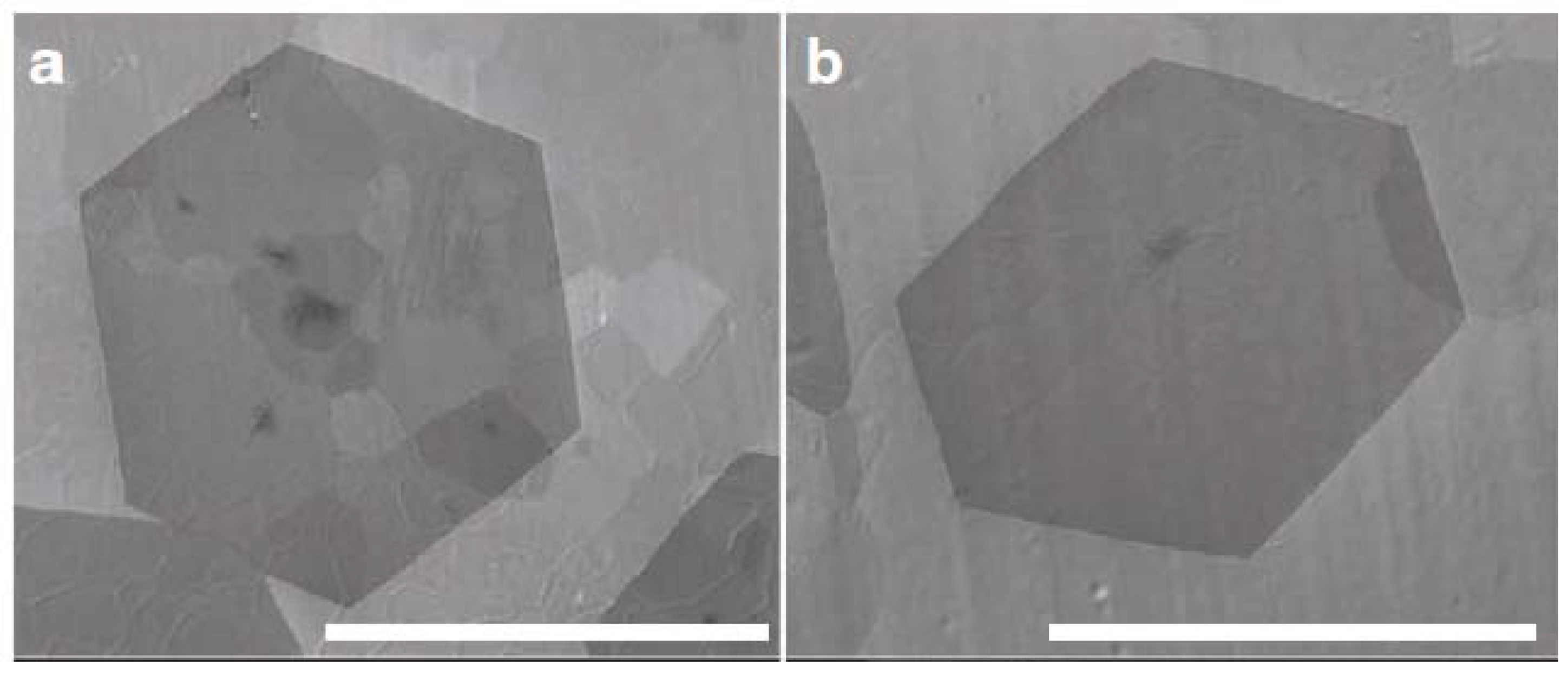
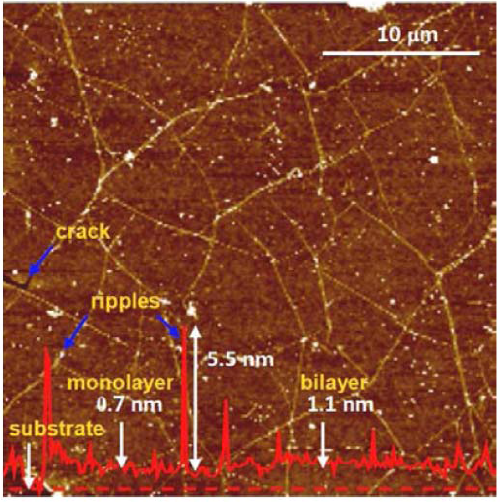
3.1.2. Chemical Vapor Deposition (CVD) Growth Films
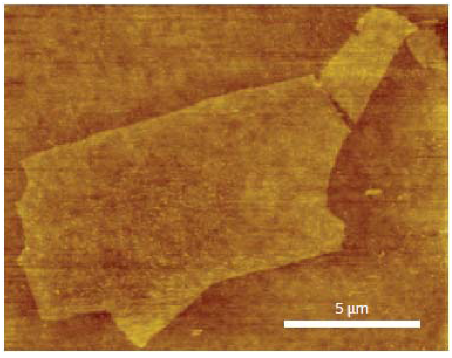
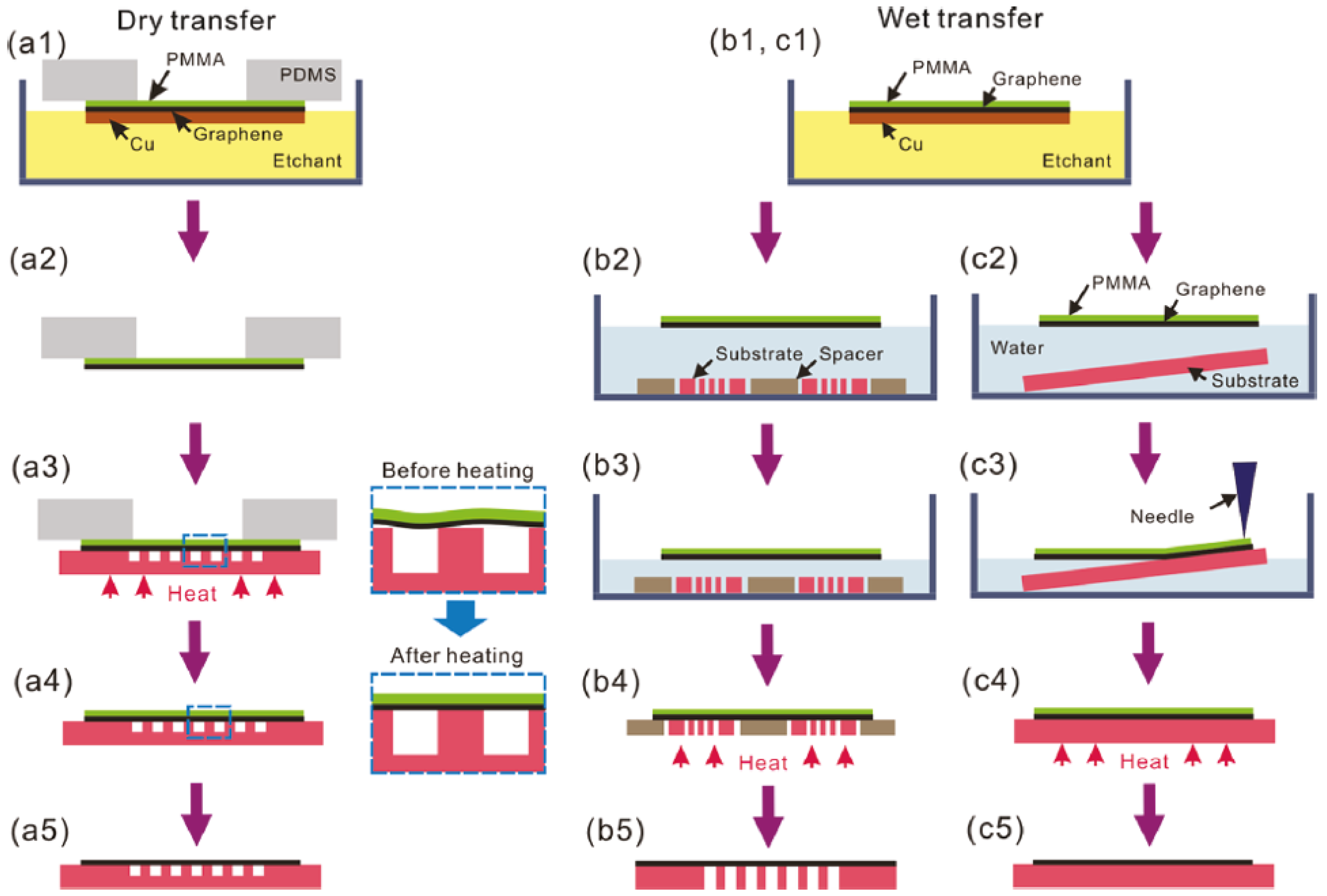
3.1.3. Transfer Printing of Graphene Films


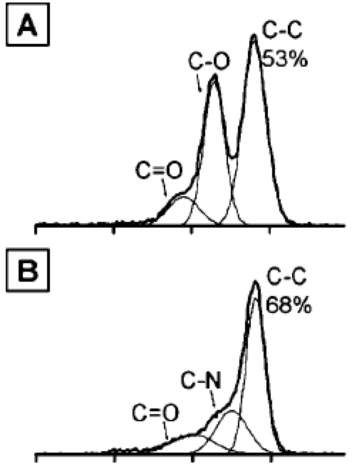
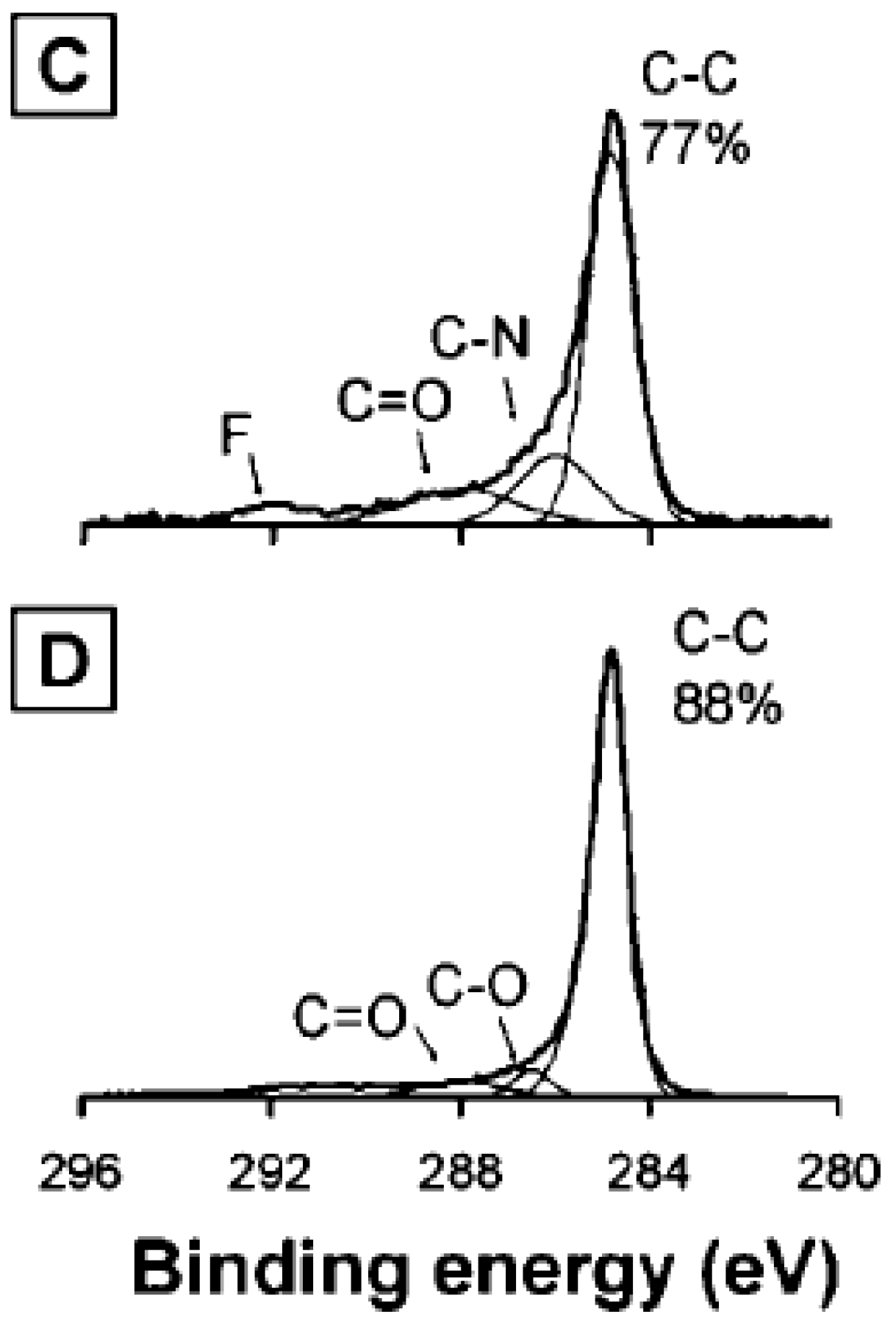
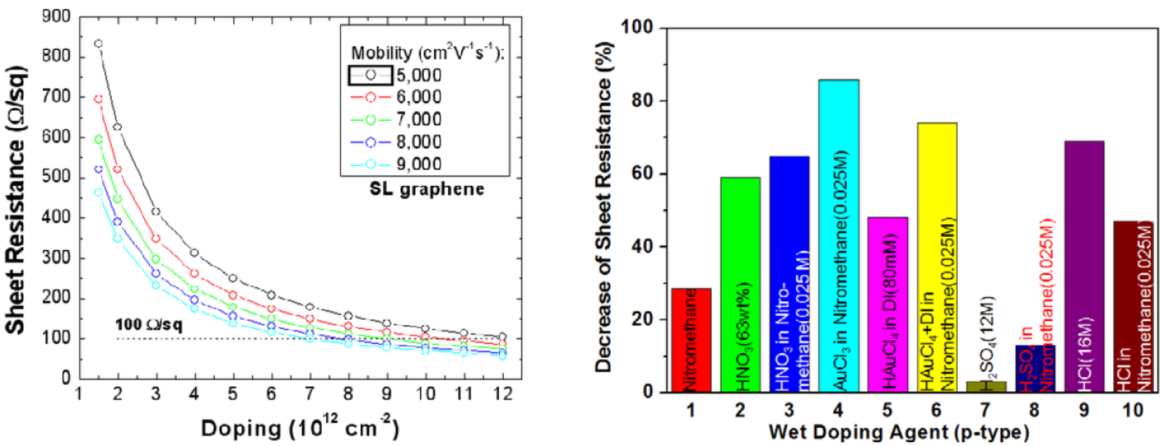
3.2. Post Treatment

4. Hybrid Films
5. Conclusions

| Material | Sheet resistance (Ω/sq) | Transmittance (%) | Reference |
|---|---|---|---|
| CNT | |||
| CVD CNT | 265 | 80 | 41 |
| CVD CNT | 265 | 70 | 42 |
| Solution CNT | 1000 | 80 | 13 |
| Solution CNT | 400 | 80 | 48 |
| Solution CNT | 100 | 70 | 63 |
| Graphene | |||
| CVD graphene | 280 | 80 | 21 |
| CVD graphene | 30 | 90 | 23 |
| CVD graphene | 980 | 97.6 | 115 |
| Reduced graphene oxide | 8000 | 93 | 84 |
| Reduced graphene oxide | 1000 | 80 | 88 |
| Reduced graphene oxide | 1800 | 70 | 94 |
| Hybrid | |||
| CNT-graphene | 240 | 85 | 128 |
| Nanowire-graphene | 64 | 94 | 130 |
| Metal grid-graphene | 20 | 90 | 132 |
| CNT-PEDOT | 80 | 75 | 134 |
Acknowledgments
Conflict of Interest
References
- Mizuhashi, M. Electrical properties of vacuum-deposited indium oxide and indium tin oxide films. Thin Solid Films 1980, 70, 91–100. [Google Scholar] [CrossRef]
- Kim, H.; Gilmore, C.M.; Pique, A.; Horwitz, J.S.; Mattoussi, H.; Murata, H.; Kafafi, Z.H.; Chrisy, D.B. Electrical, optical, and structural properties of indium-tin-oxide thin films for organic light-emitting devices. J. Appl. Phys. 1999, 86, 6451–6461. [Google Scholar] [CrossRef]
- Cairns, D.R.; Witte, R.P.; Sparacin, D.K.; Sachsman, S.M.; Paine, D.C.; Crawford, G.P.; Newton, R.R. Strain-dependent electrical resistance of tin-doped indium oxide on polymer substrates. Appl. Phys. Lett. 2000, 76, 1425. [Google Scholar] [CrossRef]
- Kirchmeyer, S.; Reuter, K. Scientific importance, properties and growing applications of Poly(3,4-ethylenedioxythiophene). J. Mater. Chem. 2005, 15, 2077–2088. [Google Scholar] [CrossRef]
- Nardes, A.M.; Kemerink, M.; de Kok, M.M.; Vinken, E.; Maturova, K.; Janssen, R.A.J. Conductivity, work function and environmental stability of pedot:pss thin films treated with sorbitol. Org. Electron. 2008, 9, 727–734. [Google Scholar] [CrossRef]
- Vitoratos, E.; Sakkopoulos, S.; Dalas, E.; Paliatsas, N.; Karageorgopoulos, D.; Petraki, F.; Kennou, S.; Choulis, S.A. Thermal degradation mechanisms of PEDOT:PSS. Org. Electron. 2009, 10, 61–66. [Google Scholar] [CrossRef]
- Lee, J.-Y.; Connor, S.T.; Cui, Y.; Peumans, P. Solution-processed metal nanowire mesh transparent electrodes. Nano Lett. 2008, 8, 689–692. [Google Scholar] [CrossRef] [PubMed]
- Wu, H.; Hu, L.; Rowell, M.W.; Kong, D.; Cha, J.J.; McDonough, J.R.; Zhu, J.; Yang, Y.; McGehee, M.D.; Cui, Y. Electrospun metal nanofiber webs as high-performance transparent electrode. Nano Lett. 2010, 10, 4242–4248. [Google Scholar] [CrossRef] [PubMed]
- Hu, L.; Kim, H.S.; Lee, J.-Y.; Peumans, P.; Cui, Y. Scalable coating and properties of transparent, flexible, silver nanowire electrodes. ACS Nano 2010, 4, 2955–2963. [Google Scholar] [CrossRef] [PubMed]
- De, S.; Higgins, T.M.; Lyons, P.E.; Doherty, E.M.; Mirmalraj, P.N.; Blau, W.J.; Boland, J.J.; Coleman, J.N. Silver nanowire networks as flexible, transparent, conducting films: Extremely high DC to optical conductivity ratios. ACS Nano 2009, 3, 1767–1774. [Google Scholar] [CrossRef] [PubMed]
- Ghosh, D.S.; Martinez, L.; Giurgola, S.; Vergani, P.; Pruneri, V. Widely transparent electrodes based on ultrathin metals. Opt. Lett. 2009, 34, 325–327. [Google Scholar] [CrossRef] [PubMed]
- Doriot-Werle, M.; Banakh, O.; Gay, P.A.; Matthey, J.; Steinmann, P.A. Tarnishing resistance of silver-palladium thin films. Surf. Coat. Technol. 2006, 200, 6696–6701. [Google Scholar] [CrossRef]
- Hu, L.; Hecht, D.S.; Gruner, G. Percolation in transparent and conducting carbon nanotube networks. Nano Lett. 2004, 4, 2513–2517. [Google Scholar] [CrossRef]
- Kaempgen, M.; Duesberg, G.S.; Roth, S. Transparent carbon nanotube coatings. Appl. Surf. Sci. 2005, 252, 425–429. [Google Scholar] [CrossRef]
- Wu, Z.C.; Chen, Z.H.; Du, X.; Logan, J.M.; Sippel, J.; Nikolou, M.; Kamaras, K.; Reynolds, J.R.; Tanner, D.B.; Hebard, A.F.; et al. Transparent, conductive carbon nanotube films. Science 2004, 305, 1273–1276. [Google Scholar] [CrossRef] [PubMed]
- Nirmalraj, P.N.; Lyons, P.E.; De, S.; Coleman, J.N.; Boland, J.J. Electrical connectivity in single-walled carbon nanotube networks. Nano Lett. 2009, 9, 3890–3895. [Google Scholar] [CrossRef] [PubMed]
- Li, Z.R.; Kandel, H.R.; Dervishi, E.; Saini, V.; Biris, A.S.; Biris, A.R.; Lupu, D. Does the wall number of carbon nanotubes matter as conductive transparent material? Appl. Phys. Lett. 2007, 91. [Google Scholar] [CrossRef]
- Hecht, D.S.; Heintz, A.M.; Lee, R.S.; Hu, L.; Moore, B.; Cucksey, C.; Risser, S. High conductivity transparent carbon nanotube films deposited from superacid. Nanotechnology 2011, 22. [Google Scholar] [CrossRef] [PubMed]
- Li, X.; Zhu, Y.; Cai, W.; Borysiak, M.; Han, B.; Chen, D.; Piner, R.D.; Colombo, L.; Ruoff, R.S. Transfer of large-area graphene films for high-performance transparent conductive electrodes. Nano Lett. 2009, 9, 4359–4363. [Google Scholar] [CrossRef] [PubMed]
- Lee, W.H.; Park, J.; Sim, S.H.; Jo, S.B.; Kim, K.S.; Hong, B.H.; Cho, K. Transparent flexible organic transistors based on monolayer graphene electrodes on plastic. Adv. Mater. 2011, 23, 1752–1756. [Google Scholar] [CrossRef] [PubMed]
- Kim, K.S.; Zhao, Y.; Jang, H.; Lee, S.Y.; Kim, J.M.; Kim, K.S.; Ahn, J.-H.; Kim, P.; Choi, J.-Y.; Hong, B.H. Large-scale pattern growth of graphene films for stretchable transparent electrodes. Nature 2009, 457, 706–710. [Google Scholar] [CrossRef] [PubMed]
- Kim, R.-H.; Bae, M.-H.; Kim, D.G.; Cheng, H.; Kim, B.H.; Kim, D.-H.; Li, M.; Wu, J.; Du, F.; Kim, H.-S.; et al. Stretchable transparent graphene interconnects for arrays of microscale inorganic light emitting diodes on rubber substrates. Nano Lett. 2011, 11, 3881–3886. [Google Scholar] [CrossRef] [PubMed]
- Bae, S.; Kim, H.; Lee, Y.; Xu, X.; Park, J.-S.; Zheng, Y.; Balakrishmam, J.; Lei, T.; Kim, H.R.; Song, Y.; et al. Roll-To-Roll Production of 30-inch graphene films for transparent electrodes. Nat. Nanotechnol. 2010, 5, 574–578. [Google Scholar] [CrossRef] [PubMed]
- White, C.T.; Todorov, T.N. Carbon nanotubes as long ballastic conductors. Nature 1998, 393, 240–242. [Google Scholar] [CrossRef]
- Quinn, B.M.; Lemay, S.G. Single-walled carbon nanotubes as templates and interconnects for nanoelectrodes. Adv. Mater. 2006, 18, 855–859. [Google Scholar] [CrossRef]
- Yao, Z.; Kane, C.L.; Dekker, C. High-field electrical transport in single-wall carbon nanotubes. Phys. Rev. Lett. 2000, 84, 2941–2944. [Google Scholar] [CrossRef] [PubMed]
- Bozovic, D.; Bockrath, M.; Hafner, J.H.; Lieber, C.M.; Park, H.; Tinkham, M. Plastic deformations in mechanically strained single-walled carbon nanotubes. Phys. Rev. B 2003, 67. [Google Scholar] [CrossRef]
- Ebbesen, T.W.; Ajayan, P.M. Large-scale synthesis of carbon nanotubes. Nature 1992, 358, 220–222. [Google Scholar] [CrossRef]
- Sadana, A.K.; Liang, F.; Brinson, B.; Arepalli, S.; Farhat, S.; Hauge, R.H.; Smalley, R.E.; Billups, W.E. Functionalization and extraction of large fullerenes and carbon-coated metal formed during the synthesis of single wall carbon nanotubes by laser oven, direct current arc, and high-pressure carbon monoxide production methods. J. Phys. Chem. B 2005, 109, 4416–4418. [Google Scholar] [CrossRef] [PubMed]
- José-Yacamán, M.; Miki-Yoshida, M.; Rendón, L.; Santiesteban, J.G. Catalytic growth of carbon microtubules with fullerene structure. Appl. Phys. Lett. 1993, 62, 657–659. [Google Scholar] [CrossRef]
- Cheng, Q.; Debnath, S.; O’Neill, L.; Hedderman, T.G.; Gregan, E.; Byrne, H.J. Systematic study of the dispersion of SWNTs in organic solvents. J. Phys. Chem. C 2010, 114, 4857–4863. [Google Scholar] [CrossRef]
- Matarredona, O.; Rhoads, H.; Li, Z.; Harwell, J.H.; Balzano, L.; Resasco, D.E. Dispersion of single-walled carbon nanotubes in aqueous solutions of the anionic surfactant NaDDBS. J. Phys. Chem. B 2003, 107, 13357–13367. [Google Scholar] [CrossRef]
- Moore, V.C.; Strano, M.S.; Haroz, E.H.; Hauge, R.H.; Smalley, R.E. Individually suspended single-walled carbon nanotubes in various surfactants. Nano Lett. 2003, 3, 1379–1382. [Google Scholar] [CrossRef]
- Lay, M.D.; Novak, J.P.; Snow, E.S. Simple route to large-scale ordered arrays of liquid-deposited carbon nanotubes. Nano Lett. 2004, 4, 603–606. [Google Scholar] [CrossRef]
- Saran, N.; Parikh, K.; Suh, D.-S.; Munoz, E.; Kolla, H.; Manohar, S.K. Fabrication and characterization of thin films of single-walled carbon nanotube bundles on flexible plastic substrates. J. Am. Chem. Soc. 2004, 126, 4462–4463. [Google Scholar] [CrossRef] [PubMed]
- Chen, J.; Rao, A.M.; Lyuksyutov, S.; Itkis, M.E.; Hamon, M.A.; Hu, H.; Cohn, R.W.; Eklund, P.C.; Colbert, D.T.; Smalley, R.E.; et al. Dissolution of full-length single-walled carbon nanotubes. J. Phys. Chem. B 2001, 105, 2525–2528. [Google Scholar] [CrossRef]
- Kaempgen, M.; Lebert, M.; Haluska, M.; Nicoloso, N.; Roth, S. Sonochemical optimization of the conductivity of single-wall carbon nanotube networks. Adv. Mater. 2008, 20, 616–620. [Google Scholar] [CrossRef]
- Wang, J.; Sun, J.; Gao, L.; Wang, Y.; Zhang, J.; Kajiura, H.; Li, Y.M.; Noda, K. Removal of the residual surfactants in transparent and conductive single-walled carbon nanotube films. J. Phys. Chem. C 2009, 113, 17685–17690. [Google Scholar] [CrossRef]
- Prisbrey, L.; Roundy, D.; Blank, K.; Fifield, L.S.; Minot, E.D. Electrical characteristics of carbon nanotube devices prepared with single oxidative point defects. J. Phys. Chem. C. 2012, 116, 1961–1965. [Google Scholar] [CrossRef] [Green Version]
- Huang, W.; Lin, Y.; Taylor, S.; Gaillard, J.; Rao, A.M.; Sun, Y.-P. Sonication-assisted functionalization and solubilization of carbon nanotubes. Nano Lett. 2002, 2, 231–234. [Google Scholar] [CrossRef]
- Cao, Q.; Hur, S.-H.; Zhu, Z.-T.; Sun, Y.; Wang, C.; Meitl, M.A.; Shim, M.; Rogers, J.A. Highly bendable, transparent thin-film transistors that use carbon-nanotube-based conductors and semiconductors with elastomeric dielectrics. Adv. Mater. 2006, 18, 304–309. [Google Scholar] [CrossRef]
- Cao, Q.; Zhu, Z.-T.; Lemaitre, M.G.; Xia, M.-G.; Shim, M.; Rogers, J.A. Transparent flexible organic thin-film transistors that use printed single-walled carbon nanotube electrodes. Appl. Phys. Lett. 2006, 88. [Google Scholar] [CrossRef]
- Bachtold, A.; Fuhrer, M.S.; Plyasunov, S.; Forero, M.; Anderson, E.H.; Zettl, A.; McEuen, P.L. Scanned probe microscopy of electronic transport in carbon nanotubes. Phys. Rev. Lett. 2000, 84, 6082–6085. [Google Scholar] [CrossRef] [PubMed]
- McEuen, P.L.; Bockrath, M.; Cobden, D.H.; Yoon, Y.-G.; Louie, S.G. Disorder, pseudospins, and backscattering in carbon nanotubes. Phys. Rev. Lett. 1999, 83, 5098–5101. [Google Scholar] [CrossRef]
- Ho, X.; Ye, L.; Rotkin, S.V.; Cao, Q.; Unarunotai, S.; Salamat, S.; Alam, M.A.; Rogers, J.A. Scaling properties in transistors that use aligned arrays of single-walled carbon nanotubes. Nano Lett. 2010, 10, 499–503. [Google Scholar] [CrossRef] [PubMed]
- Park, J.-Y.; Rosenblatt, S.; Yaish, Y.; Sazonova, V.; Ustunel, H.; Braig, S.; Arias, T.A.; Brouwer, P.W.; McEuen, P.L. Electron-phonon scattering in metallic single-walled carbon nanotubes. Nano Lett. 2004, 4, 517–520. [Google Scholar] [CrossRef]
- Javey, A.; Guo, J.; Paulsson, M.; Wang, Q.; Mann, D.; Lundstrom, M.; Dai, H. High-field quasiballistic transport in short carbon nanotubes. Phys. Rev. Lett. 2004, 92, 106804:1–106804:4. [Google Scholar] [CrossRef]
- Green, A.A.; Hersam, M.C. Colored semitransparent conductive coatings consisting of monodisperse metallic single-walled carbon nanotubes. Nano Lett. 2008, 8, 1417–1422. [Google Scholar] [CrossRef] [PubMed]
- Fuhrer, M.S.; Nygard, J.; Shih, L.; Forero, M.; Yoon, Y.-G.; Mazzoni, M.S.C.; Choi, H.J.; Ihm, J.; Louie, S.G.; Zettl, A.; et al. Crossed nanotube junctions. Science 2000, 288, 494–497. [Google Scholar] [CrossRef] [PubMed]
- Wang, C.; Cao, Q.; Ozel, T.; Gaur, A.; Rogers, J.A.; Shim, M. Electronically selective chemical functionalization of carbon nanotubes: Correlation between raman spectral and electrical responses. J. Am. Chem. Soc. 2005, 127, 11460–11468. [Google Scholar] [CrossRef] [PubMed]
- Strano, M.S.; Dyke, C.A.; Usrey, M.L.; Barone, P.W.; Allen, M.J.; Shan, H.; Kittrell, C.; Hauge, R.H.; Tour, J.M.; Smalley, R.E. Electronic structure control of single-walled carbon nanotube functionalization. Science 2003, 301, 1519–1522. [Google Scholar] [CrossRef] [PubMed]
- Collins, P.C.; Arnold, M.S.; Avouris, P. Engineering carbon nanotubes and nanotube circuits using electrical breakdown. Science 2001, 292, 706–709. [Google Scholar] [CrossRef] [PubMed]
- Arnold, M.S.; Green, A.A.; Hulvat, J.F.; Stupp, S.I.; Hersam, M.C. Sorting carbon nanotubes by electronic structure using density differentiation. Nat. Nanotechnol. 2006, 1, 60–65. [Google Scholar] [CrossRef] [PubMed]
- Hersam, M.C. Progress towards monodisperse single-walled carbon nanotubes. Nat. Nanotechnol. 2008, 3, 387–394. [Google Scholar] [CrossRef]
- Krupke, R.; Linden, S.; Rapp, M.; Hennrich, F. Thin films of metallic carbon nanotubes prepared by dielectrophoresis. Adv. Mater. 2006, 18, 1468–1470. [Google Scholar] [CrossRef]
- Zhou, X.; Park, J.-Y.; Huang, S.; Liu, J.; McEuen, P.L. Band structure, phonon scattering, and the performance limit of single-walled carbon nanotube transistors. Phys. Rev. Lett. 2005, 95. [Google Scholar] [CrossRef] [PubMed]
- Islam, A.E.; Du, F.; Ho, X.; Jin, S.H.; Dunham, S.; Rogers, J.A. Effect of variations in diameter and density on the statistics of aligned array carbon-nanotube field effect transistors. J. Appl. Phy. 2012, 111. [Google Scholar] [CrossRef]
- Li, Y.; Kim, W.; Zhang, Y.; Rolandi, M.; Wang, D.; Dai, H. Growth of single-walled carbon nanotubes from discrete catalytic nanoparticles of various sizes. J. Phys. Chem. B 2001, 105, 11424–11431. [Google Scholar] [CrossRef]
- Cheung, C.L.; Kurtz, A.; Park, H.; Lieber, C.M. Diameter-controlled synthesis of carbon nanotubes. J. Phys. Chem. B 2002, 106, 2429–2433. [Google Scholar] [CrossRef]
- Bachilo, S.M.; Balzano, L.; Herrera, J.E.; Pompeo, F.; Resasco, D.E.; Weisman, R.B. Narrow (n,m)-distribution of single-walled carbon nanotubes grown using a solid supported catalyst. J. Am. Chem. Soc. 2003, 125, 11186–11187. [Google Scholar] [CrossRef] [PubMed]
- Ryu, K.; Badmaev, A.; Gomez, L.; Ishikawa, F.; Lei, B.; Zhou, C. Synthesis of aligned single-walled nanotubes using catalysts defined by nanosphere lithography. J. Am. Chem. Soc. 2007, 129, 10104–10105. [Google Scholar] [CrossRef] [PubMed]
- Hecht, D.; Hu, L.; Gruner, G. Conductivity scaling with bundle length and diameter in single walled carbon nanotube networks. Appl. Phys. Lett. 2006, 89. [Google Scholar] [CrossRef]
- De, S.; King, P.J.; Lyons, P.E.; Khan, U.; Coleman, J.N. Size effects and the problem with percolation in nanostructured transparent conductors. ACS Nano 2010, 4, 7064–7072. [Google Scholar] [CrossRef] [PubMed]
- Lim, C.; Min, D.-H.; Leea, S.-B. Direct patterning of carbon nanotube network devices by selective vacuum filtration. Appl. Phys. Lett. 2007, 91. [Google Scholar] [CrossRef]
- Liu, Q.; Fujigaya, T.; Cheng, H.-M.; Nakashima, N. Free-standing highly conductive transparent ultrathin single-walled carbon nanotube films. J. Am. Chem. Soc. 2010, 132, 16581–16586. [Google Scholar] [CrossRef] [PubMed]
- Tenet, R.C.; Barnes, T.M.; Bergeson, J.D.; Ferguson, A.J.; To, B.; Gedvilas, L.M.; Heben, M.J.; Blackburn, J.L. Ultrasmooth, large-area, high-uniformity, conductive transparent single-walled-carbon-nanotube films for photovoltaics produced by ultrasonic spraying. Adv. Mater. 2009, 21, 3210–3216. [Google Scholar] [CrossRef]
- Meitl, M.A.; Zhou, Y.; Gaur, A.; Jeon, S.; Usrey, M.L.; Strano, M.S.; Rogers, J.A. Solution casting and transfer printing single-walled carbon nanotube films. Nano Lett. 2004, 4, 1643–1647. [Google Scholar] [CrossRef]
- Park, J.-U.; Meitl, M.A.; Hur, S.-H.; Usrey, M.L.; Strano, M.S.; Kenis, P.J.A.; Rogers, J.A. In situ deposition and patterning of single-walled carbon nanotubes by laminar flow and controlled flocculation in microfluidic channels. Angew. Chem. Int. Ed. 2006, 45, 581–585. [Google Scholar] [CrossRef]
- Zhou, Y.; Hu, L.; Grüner, G. A method of printing carbon nanotube thin films. Appl. Phys. Lett. 2006, 88. [Google Scholar] [CrossRef]
- Jin, C.; Suenaga, K.; Iijima, S. Plumbing carbon nanotubes. Nat. Nanotechnol. 2008, 3, 17–21. [Google Scholar] [CrossRef] [PubMed]
- Banhart, F. The formation of a connection between carbon nanotubes in an electron beam. Nano Lett. 2001, 1, 329–332. [Google Scholar] [CrossRef]
- Dyke, C.A.; Tour, J.M. Unbundled and highly functionalized carbon nanotubes from aqueous reactions. Nano Lett. 2003, 3, 1215–1218. [Google Scholar] [CrossRef]
- Geng, H.-Z.; Kim, K.K.; So, K.P.; Lee, Y.S.; Chang, Y.; Lee, Y.H. Effect of acid treatment on carbon nanotube-based flexible transparent conducting films. J. Am. Chem. Soc. 2007, 129, 7758–7759. [Google Scholar] [CrossRef] [PubMed]
- Lee, R.S.; Kim, H.J.; Fischer, J.E.; Thess, A.; Smalley, R.E. Conductivity enhancement in single-walled carbon nanotube bundles doped with K and Br. Nature 1997, 388, 255–257. [Google Scholar] [CrossRef]
- Kong, J.; Franklin, N.R.; Zhou, C.; Chapline, M.G.; Peng, S.; Cho, K.; Dai, H. Nanotube molecular wires as chemical sensors. Science 2000, 287, 622–625. [Google Scholar] [CrossRef] [PubMed]
- Jackson, R.; Domercq, B.; Jain, R.; Kippelen, B.; Graham, S. Stability of doped transparent carbon nanotube electrodes. Adv. Funct. Mater. 2008, 18, 2548–2554. [Google Scholar] [CrossRef]
- Skakalova, V.; Kaiser, A.B.; Dettlaff-Weglikowska, U.; Hrncarikova, K.; Roth, S. Effect of chemical treatment on electrical conductivity, infrared absorption, and Raman spectra of single-walled carbon nanotubes. J. Phys. Chem. B 2005, 109, 7174–7181. [Google Scholar] [CrossRef] [PubMed]
- Takenobu, T.; Kanbara, T.; Akima, N.; Takahashi, T.; Shiraishi, M.; Tsukagoshi, K.; Kataura, H.; Aoyagi, Y.; Iwasa, Y. Control of carrier density by a solution method in carbon-nanotube devices. Adv. Mater. 2005, 17, 2430–2434. [Google Scholar] [CrossRef]
- Abdula, D.; Shim, M. Performance and photovoltaic response of polymer-doped carbon nanotube p-n diodes. ACS Nano 2008, 2, 2154–2159. [Google Scholar] [CrossRef] [PubMed]
- Du, X.; Skachko, I.; Barker, A.; Andrei, E.Y. Approaching ballistic transport in suspended graphene. Nat. Nanotechnol. 2008, 3, 491–495. [Google Scholar] [CrossRef] [PubMed]
- Nair, R.R.; Blake, P.; Grigorenko, A.N.; Novoselov, K.S.; Booth, T.J.; Stauber, T.; Peres, N.M.R.; Geim, A.K. Fine structure constant defines visual transparency of graphene. Science 2008, 320. [Google Scholar] [CrossRef] [PubMed]
- Eda, G.; Fanchini, G.; Chhowalla, M. Large-area ultrathin films of reduced graphene oxide as a transparent and flexible electronic material. Nat. Nanotechnol. 2008, 3, 270–274. [Google Scholar] [CrossRef] [PubMed]
- Hernandez, Y.; Nicolosi, V.; Lotya, M.; Blighe, F.M.; Sun, Z.; De, S.; McGovern, I.T.; Holland, B.; Byrne, M.; Gun’ko, Y.K.; et al. High-yield production of graphene by liquid-phase exfoliation of graphite. Nat. Nanotechnol. 2008, 3, 563–568. [Google Scholar] [CrossRef] [PubMed]
- Li, X.; Zhang, G.; Bai, X.; Sun, X.; Wang, X.; Wang, E.; Dai, H. Highly conducting graphene sheets and langmuir-blodgett films. Nat. Nanotechnol. 2008, 3, 538–542. [Google Scholar] [CrossRef] [PubMed]
- Lotya, M.; Hernandez, Y.; King, P.J.; Smith, R.J.; Nicolosi, V.; Karlsson, L.S.; Blighe, F.M.; De, S.; Wang, Z.; McGovern, I.T.; et al. Liquid phase production of graphene by exfoliation of graphite in surfactant / water solutions. J. Am. Chem. Soc. 2009, 131, 3611–3620. [Google Scholar] [CrossRef] [PubMed]
- De, S.; King, P.J.; Lotya, M.; O’Neill, A.; Doherty, E.M.; Hernandez, Y.; Duesberg, G.S.; Coleman, J.N. Flexible, transparent, conducting films of randomly stacked graphene from surfactant-stabilized, oxide-free graphene dispersions. Small 2010, 6, 458–464. [Google Scholar] [CrossRef] [PubMed]
- Tung, V.C.; Allen, M.J.; Yang, Y.; Kaner, R.B. High-throughput solution processing of large-scale graphene. Nat. Nanotechnol. 2009, 4, 25–29. [Google Scholar] [CrossRef] [PubMed]
- Becerril, H.A.; Mao, J.; Liu, Z.; Stoltenberg, R.M.; Bao, Z.; Chen, Y. Evaluation of solution-processed reduced graphene oxide films as transparent conductors. ACS Nano 2008, 2, 463–470. [Google Scholar] [CrossRef]
- Park, S.; An, J.; Jung, I.; Piner, R.D.; An, S.J.; Li, X.; Velamakanni, A.; Ruoff, R.S. Colloidal suspensions of highly reduced graphene oxide in a wide variety of organic solvents. Nano Lett. 2009, 9, 1593–1597. [Google Scholar] [CrossRef] [PubMed]
- Cote, L.J.; Kim, F.; Huang, J. Langmuir-blodgett assembly of graphite oxide single layers. J. Am. Chem. Soc. 2009, 131, 1043–1049. [Google Scholar] [CrossRef] [PubMed]
- Dikin, D.A.; Stankovich, S.; Zimney, E.J.; Piner, R.D.; Dommett, G.H.B.; Evmenenko, G.; Nguyen, S.T.; Ruoff, R.S. Preparation and characterization of graphene oxide paper. Nature 2007, 448, 457–460. [Google Scholar] [CrossRef] [PubMed]
- Gilje, S.; Han, S.; Wang, M.S.; Wang, K.L.; Kaner, R.B. A Chemical route to graphene for device applications. Nano Lett. 2007, 7, 3394–3398. [Google Scholar] [CrossRef] [PubMed]
- Li, D.; Muller, M.B.; Gilje, S.; Kaner, R.B.; Wallace, G.G. Processable aqueous dispersions of graphene nanosheets. Nat. Nanotechnol. 2008, 3, 101–105. [Google Scholar] [CrossRef] [PubMed]
- Wang, X.; Zhi, L.J.; Mullen, K. Transparent, conductive graphene electrodes for dye-sensitized solar cells. Nano Lett. 2008, 8, 323–327. [Google Scholar] [CrossRef] [PubMed]
- Gomez-Navarro, C.; Weitz, R.T.; Bittner, A.M.; Scolari, M.; Mews, A.; Burghard, M.; Kern, K. Electronic transport properties of individual chemically reduced graphene oxide sheets. Nano Lett. 2007, 7, 3499–3503. [Google Scholar] [CrossRef] [PubMed]
- Hecht, D.S.; Hu, L.; Irvin, G. Emerging transparent electrodes based on thin films of carbon nanotubes, graphene and metallic nanostructures. Adv. Mater. 2011, 23, 1482–1513. [Google Scholar] [CrossRef] [PubMed]
- Hummers, W.S.; Offeman, R.E. Preparation of graphitic oxide. J. Am. Chem. Soc. 1958, 80, 1339. [Google Scholar] [CrossRef]
- Park, S.; An, J.; Piner, R.D.; Jung, I.; Yang, D.; Velamakanni, A.; Nguyen, S.T.; Ruoff, R.S. Aqueous suspension and characterization of chemically modified graphene sheets. Chem. Mater. 2008, 20, 6592–6594. [Google Scholar] [CrossRef]
- Donner, S.; Li, H.W.; Yeung, E.S.; Porter, M.D. Fabrication of optically transparent carbon electrodes by the pyrolysis of photoresist films: approach to single-molecule spectroelectrochemistry. Anal. Chem. 2006, 78, 2816–2822. [Google Scholar] [CrossRef] [PubMed]
- Mattevi, C.; Eda, G.; Agnoli, S.; Miller, S.; Mkhoyan, K.A.; Celik, O.; Mastrogiovanni, D.; Granozzi, G.; Garfunkel, E.; Chhowalla, M. Evolution of electrical, chemical, and structural properties of transparent and conducting chemically derived graphene thin films. Adv. Funct. Mater. 2009, 19, 2577–2583. [Google Scholar] [CrossRef]
- Yu, Q.; Jauregui, L.A.; Wu, W.; Colby, R.; Tian, J.; Su, Z.; Cao, H.; Liu, Z.; Pandey, D.; Wei, D.; et al. Control and characterization of individual grains and grain boundaries in graphene grown by chemical vapor deposition. Nat. Mater. 2011, 10, 443–449. [Google Scholar] [CrossRef] [PubMed]
- Koepke, J.C.; Wood, J.D.; Estrada, D.; Ong, Z.-Y.; He, K.T.; Pop, E.; Lyding, J.W. Atomic-scale evidence for potential barriers and strong carrier scattering at graphene grain boundaries: A scanning tunneling microscopy study. ACS Nano 2013, 7, 75–86. [Google Scholar] [CrossRef] [PubMed]
- Vlassiouk, I.; Regmi, M.; Fulvio, P.; Dai, S.; Datskos, P.; Eres, G.; Smirnov, S. Role of hydrogen in chemical vapor deposition growth of large single-crystal graphene. ACS Nano 2011, 5, 6069–6076. [Google Scholar] [CrossRef] [PubMed]
- Li, X.; Magnuson, C.W.; Venugopal, A.; An, J.; Suk, J.W.; Han, B.; Borysiak, M.; Cai, W.; Velamakanni, A.; Zhu, Y.; et al. Graphene films with large domain size by a two-step chemical vapor deposition process. Nano Lett. 2010, 10, 4328–4334. [Google Scholar] [CrossRef] [PubMed]
- Wu, T.; Ding, G.; Shen, H.; Wang, H.; Sun, L.; Jiang, D.; Xie, X.; Jiang, M. Triggering the continuous growth of graphene toward millimeter-sized grains. Adv. Funct. Mater. 2013, 23, 198–203. [Google Scholar] [CrossRef]
- Wang, H.; Wang, G.; Bao, P.; Yang, S.; Zhu, W.; Xie, X.; Zhang, W.-J. Controllable synthesis of submillimeter single-crystal monolayer graphene domains on copper foils by suppressing nucleation. J. Am. Chem. Soc. 2012, 134, 3627–3630. [Google Scholar] [CrossRef] [PubMed]
- Li, X.; Magnuson, C.W.; Venugopal, A.; Tromp, R.M.; Hannon, J.B.; Vogel, E.M.; Colombo, L.; Ruoff, R.S. Large-area graphene single crystals grown by low-pressure chemical vapor deposition of methane on copper. J. Am. Chem. Soc. 2011, 133, 2816–2819. [Google Scholar] [CrossRef] [PubMed]
- Gao, L.; Ren, W.; Xu, H.; Jin, L.; Wang, Z.; Ma, T.; Ma, L.-P.; Zhang, Z.; Fu, Q.; Peng, L.-M.; et al. Repeated growth and bubbling transfer of graphene with millimetre-size single-crystal grains using platinum. Nat. Commun. 2012, 3. [Google Scholar] [CrossRef]
- Chae, S.J.; Gunes, F.; Kim, K.K.; Kim, E.S.; Han, G.H.; Kim, S.M.; Shin, H.-J.; Yoon, S.-M.; Choi, J.-Y.; Park, M.H.; et al. Synthesis of large-area graphene layers on poly-nickel substrate by chemical vapor deposition: wrinkle formation. Adv. Mater. 2009, 21, 2328–2333. [Google Scholar] [CrossRef]
- Zhu, W.; Low, T.; Perebeinos, V.; Bol, A.A.; Zhu, Y.; Yan, H.; Tersoff, J.; Avouris, P. Structure and electronic transport in graphene wrinkles. Nano Lett. 2012, 12, 3431–3436. [Google Scholar] [CrossRef] [PubMed]
- Hattab, H.; N’Diaye, A.T.; Wall, D.; Klein, C.; Jnawali, G.; Coraux, J.; Busse, C.; van Gastel, R.; Poelsema, B.; Michely, T.; et al. Interplay of wrinkles, strain, and lattice parameter in graphene on iridium. Nano Lett. 2012, 12, 678–682. [Google Scholar] [CrossRef] [PubMed]
- Zhang, Y.; Gao, T.; Gao, Y.; Xie, S.; Ji, Q.; Yan, K.; Peng, H.; Liu, Z. Defect-like structures of graphene on copper foils for strain relief investigated by high-resolution scanning tunneling microscopy. ACS Nano 2011, 5, 4014–4022. [Google Scholar] [CrossRef] [PubMed]
- Lee, Y.; Bae, S.; Jang, H.; Jang, S.; Zhu, S.-E.; Sim, S.H.; Song, Y., II; Hong, B.H.; Ahn, J.-H. Wafer-scale synthesis and transfer of graphene films. Nano Lett. 2010, 10, 490–493. [Google Scholar] [CrossRef] [PubMed]
- Liang, X.; Sperling, B.A.; Calizo, I.; Cheng, G.; Hacker, C.A.; Zhang, Q.; Obeng, Y.; Yan, K.; Peng, H.; Li, Q.; et al. Toward clean and crackless transfer of graphene. ACS Nano 2011, 5, 9144–9153. [Google Scholar] [CrossRef] [PubMed]
- Suk, J.W.; Kitt, A.; Magnuson, C.W.; Hao, Y.; Ahmed, S.; An, J.; Swan, A.K.; Goldberg, B.B.; Ruoff, R.S. Transfer of CVD-grown monolayer graphene onto arbitrary substrates. ACS Nano 2011, 5, 6916–6924. [Google Scholar] [CrossRef] [PubMed]
- Unarunotai, S.; Murata, Y.; Chialvo, C.E.; Kim, H.-S.; MacLaren, S.; Mason, N.; Petrov, I.; Rogers, J.A. Transfer of graphene layers grown on SiC wafers to other substrates and their integration into field effect transistors. Appl. Phy. Lett. 2009, 95. [Google Scholar] [CrossRef]
- Unarunotai, S.; Koepke, J.C.; Tsai, C.-L.; Du, F.; Chialvo, C.E.; Murata, Y.; Haasch, R.; Petrov, I.; Mason, N.; et al. Layer-by-layer transfer of multiple, large area sheets of graphene grown in multilayer stacks on a single SiC wafer. ACS Nano 2010, 4, 5591–5598. [Google Scholar] [CrossRef] [PubMed]
- Wang, Y.; Zheng, Y.; Xu, X.; Dubuisson, E.; Bao, Q.; Lu, J.; Loh, K.P. Electrochemical delamination of CVD grown graphene film: Toward the recyclable use of copper catalyst. ACS Nano 2011, 5, 9927–9933. [Google Scholar] [CrossRef] [PubMed]
- De la Rosa, C.J.L.; Sun, J.; Lindvall, N.; Cole, M.T.; Nam, Y.; Loffler, M.; Olsson, E.; Teo, K.B.K.; Yurgens, A. Frame assisted H2O electrolysis induced H2 bubbling transfer of large area graphene grown by chemical vapor deposition on Cu. Appl. Phy. Lett. 2013, 102. [Google Scholar] [CrossRef]
- Kobayashi, T.; Bando, M.; Kimura, N.; Shimizu, K.; Kadono, K.; Umezu, N.; Miyahara, K.; Hayazaki, S.; Nagai, S.; Mizuguchi, Y.; et al. Production of a 100-m-long high-quality Graphene transparent conductive film by roll-to-roll chemical vapor deposition and transfer process. Appl. Phy. Lett. 2013, 102. [Google Scholar] [CrossRef]
- Yan, C.; Kim, K.-S.; Lee, S.-K.; Bae, S.-H.; Hong, B.H.; Kim, J.-H.; Lee, H.-J.; Ahn, J.-H. Mechanical and environmental stability of polymer thin-film-coated graphene. ACS Nano 2012, 6, 2096–2103. [Google Scholar] [CrossRef] [PubMed]
- Han, T.-H.; Lee, Y.; Choi, M.-R.; Woo, S.-H.; Bae, S.-H.; Hong, B.H.; Ahn, J.-H.; Lee, T.-W. Extremely efficient flexible organic light-emitting diodes with modified graphene anode. Nat. Photonics 2012, 6, 105–110. [Google Scholar] [CrossRef]
- Wehling, T.O.; Novoselov, K.S.; Morozov, S.V.; Vdovin, E.E.; Katsnelson, M.I.; Geim, A.K.; Lichtenstein, A.I. Molecular doping of graphene. Nano Lett. 2008, 8, 173–177. [Google Scholar] [CrossRef] [PubMed] [Green Version]
- Hellstrom, S.L.; Vosgueritchian, M.; Stoltenberg, R.M.; Irfan, I.; Hammock, M.; Wang, Y.B.; Jia, C.; Guo, X.; Gao, Y.; Bao, Z. Strong and Stable doping of carbon nanotubes and graphene by MoOx for transparent electrodes. Nano Lett. 2012, 12, 3574–3580. [Google Scholar] [CrossRef] [PubMed]
- Lee, B.; Chen, Y.; Duerr, F.; Mastrogiovanni, D.; Garfunkel, E.; Andrei, E.Y.; Podzorov, V. Modification of electronic properties of graphene with self-assembled monolayers. Nano Lett. 2010, 10, 2427–2432. [Google Scholar] [CrossRef] [PubMed]
- Ni, G.-X.; Zheng, Y.; Bae, S.; Tan, C.Y.; Kahya, O.; Wu, J.; Hong, B.H.; Yao, K.; Ozyilmaz, B. Graphene_ferroelectric hybrid structure for flexible transparent electrodes. ACS Nano 2012, 6, 3935–3942. [Google Scholar] [CrossRef] [PubMed]
- Blake, P.; Brimicombe, P.D.; Nair, R.R.; Booth, T.J.; Jiang, D.; Schedin, F.; Ponomarenko, L.A.; Morozov, S.V.; Gleeson, H.F.; Hill, E.W.; et al. Graphene-based liquid crystal device. Nano Lett. 2008, 8, 1704–1708. [Google Scholar] [CrossRef] [PubMed]
- Tung, V.C.; Chen, L.-M.; Allen, M.J.; Wassei, J.K.; Nelson, K.; Kaner, R.B.; Yang, Y. Low-temperature solution processing of graphene-carbon nanotube hybrid materials for high-performance transparent conductors. Nano Lett. 2009, 9, 1949–1955. [Google Scholar] [CrossRef] [PubMed]
- Kim, Y.-K.; Min, D.-H. Durable large-area thin films of graphene/carbon nanotube double layers as a transparent electrode. Langmuir 2009, 25, 11302–11306. [Google Scholar] [CrossRef] [PubMed]
- Kholmanov, I.N.; Magnuson, C.W.; Aliev, A.E.; Li, H.; Zhang, B.; Suk, J.W.; Zhang, L.L.; Peng, E.; Mousavi, S.H.; Khanikaev, A.B.; et al. Improved electrical conductivity of graphene films integrated with metal nanowires. Nano Lett. 2012, 12, 5679–5683. [Google Scholar] [CrossRef]
- Jeong, C.; Nair, P.; Khan, M.; Lundstrom, M.; Alam, M.A. Prospects for nanowire-doped polycrystalline graphene films for ultratransparent, highly conductive electrodes. Nano Lett. 2011, 11, 5020–5025. [Google Scholar] [CrossRef] [PubMed]
- Zhu, Y.; Sun, Z.; Yan, Z.; Jin, Z.; Tour, J.M. Rational design of hybrid graphene films for high-performance transparent electrodes. ACS Nano 2011, 5, 6472–6479. [Google Scholar] [CrossRef] [PubMed]
- Ho, X.; Lu, H.; Liu, W.; Tey, J.N.; Cheng, C.K.; Wei, J. Electrical and optical properties of hybrid transparent electrodes that use metal grids and graphene films. J. Mater. Res. 2013, 28, 620–626. [Google Scholar] [CrossRef]
- De, S.; Lyons, P.E.; Sorel, S.; Doherty, E.M.; King, P.J.; Blau, W.J.; Nirmalraj, P.N.; Boland, J.J.; Scardaci, V.; Joimel, J.; et al. Transparent, flexible, and highly conductive thin films based on polymer nanotube composites. ACS Nano 2009, 3, 714–720. [Google Scholar] [CrossRef] [PubMed]
© 2013 by the authors; licensee MDPI, Basel, Switzerland. This article is an open access article distributed under the terms and conditions of the Creative Commons Attribution license (http://creativecommons.org/licenses/by/3.0/).
Share and Cite
Ho, X.; Wei, J. Films of Carbon Nanomaterials for Transparent Conductors. Materials 2013, 6, 2155-2181. https://doi.org/10.3390/ma6062155
Ho X, Wei J. Films of Carbon Nanomaterials for Transparent Conductors. Materials. 2013; 6(6):2155-2181. https://doi.org/10.3390/ma6062155
Chicago/Turabian StyleHo, Xinning, and Jun Wei. 2013. "Films of Carbon Nanomaterials for Transparent Conductors" Materials 6, no. 6: 2155-2181. https://doi.org/10.3390/ma6062155