Full-Field Strain Mapping at a Ge/Si Heterostructure Interface

Abstract
:
1. Introduction
2. Theory
2.1. Strain of Edge Dislocation Given by Peierls-Nabarro Model
2.2. Strain of Edge Dislocation Given by Foreman Model
3. Experimental Methods
3.1. Specimen Preparation
3.2. Electron Microscopy
3.3. Geometric Phase Analysis
3.4. Peak Pairs Analysis
4. Results and Discussion
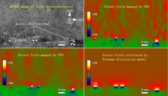
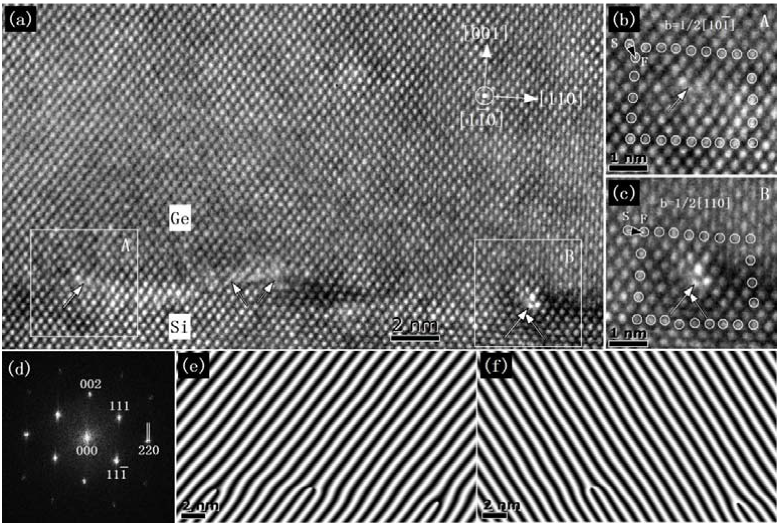
4.1. Type of Misfit Dislocations at the Ge/Si Heterostructure Interface


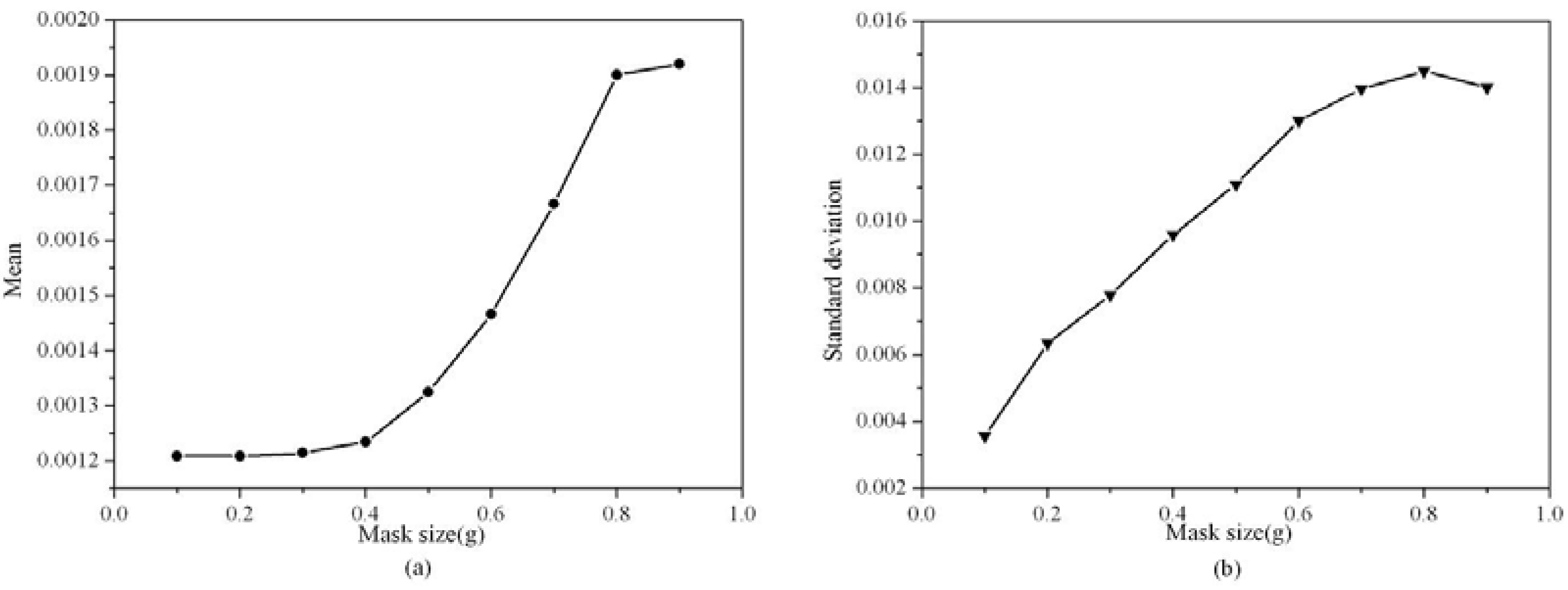
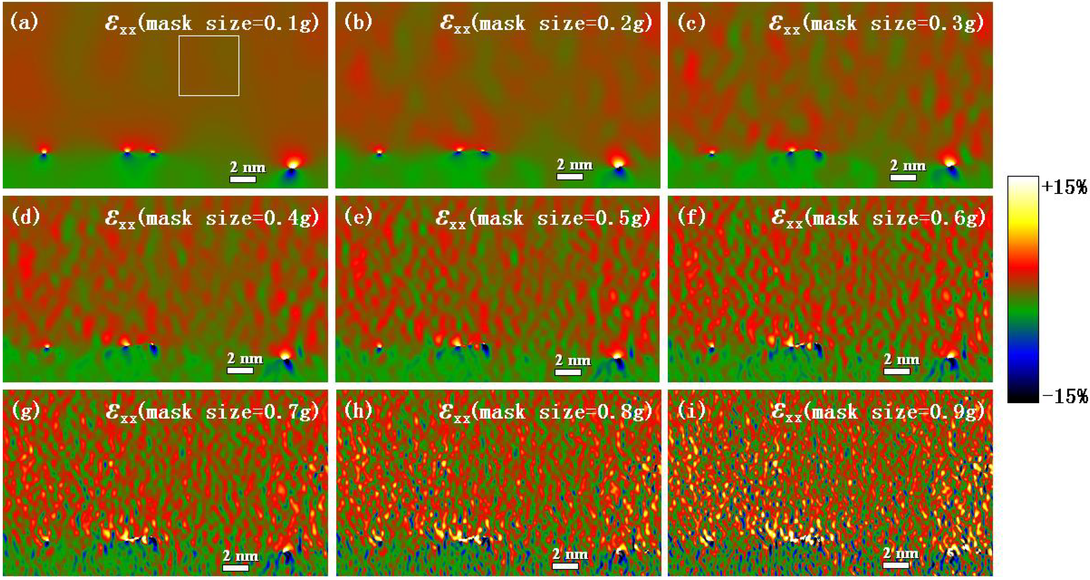
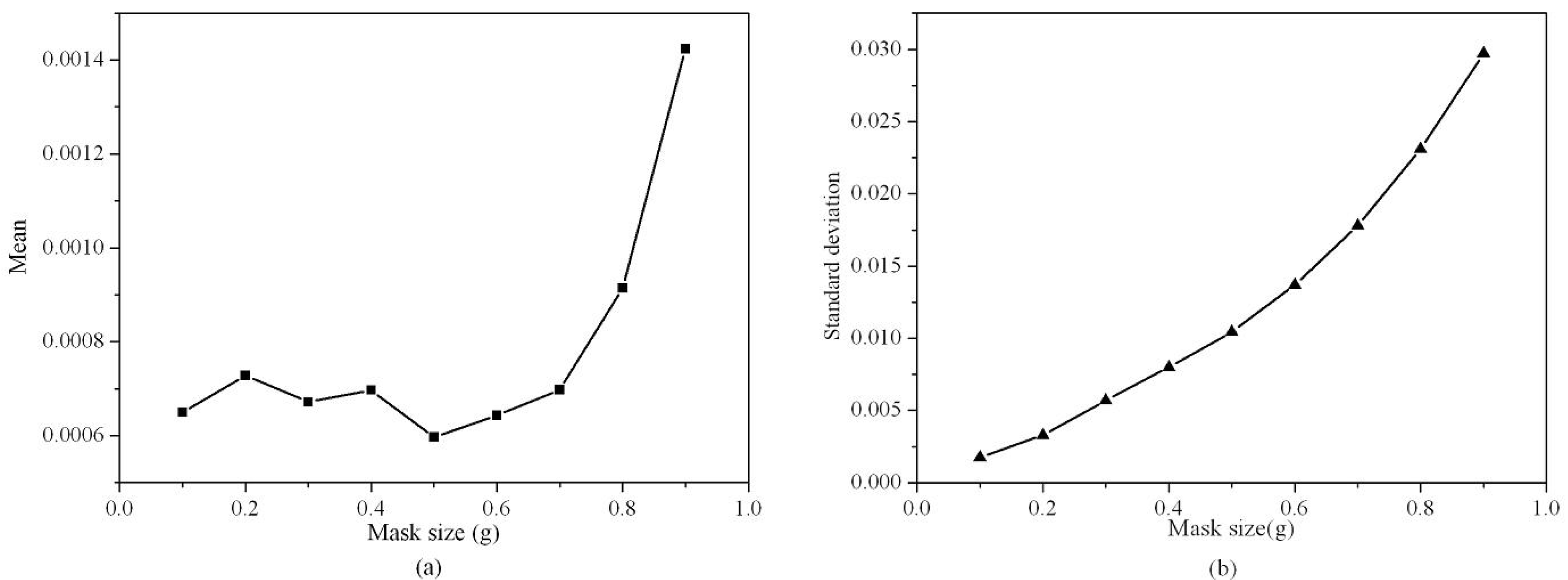
4.2. Effect of Mask Size on the Strain Calculation Results with GPA

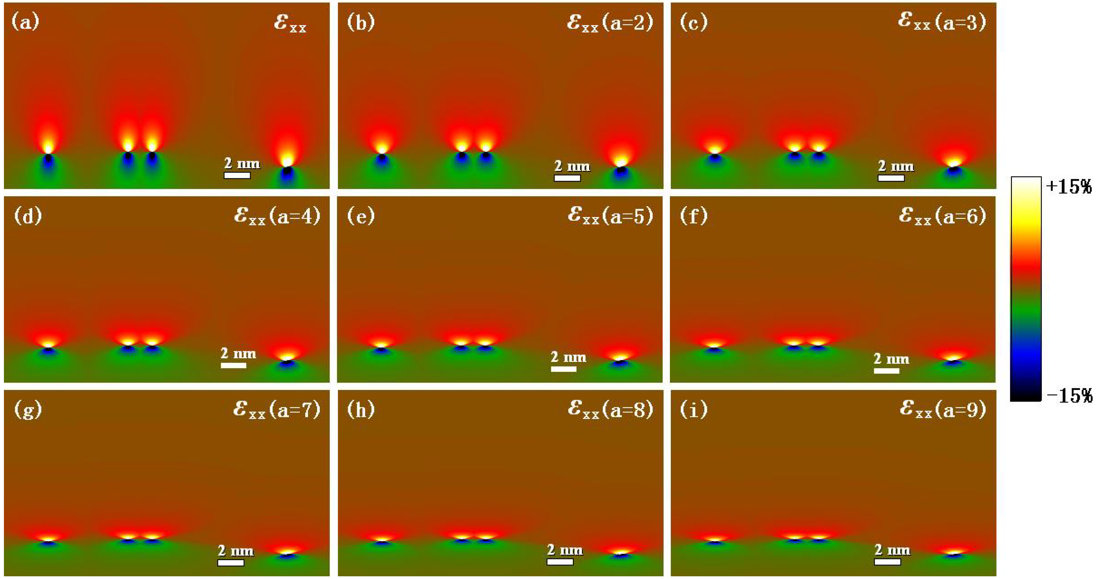
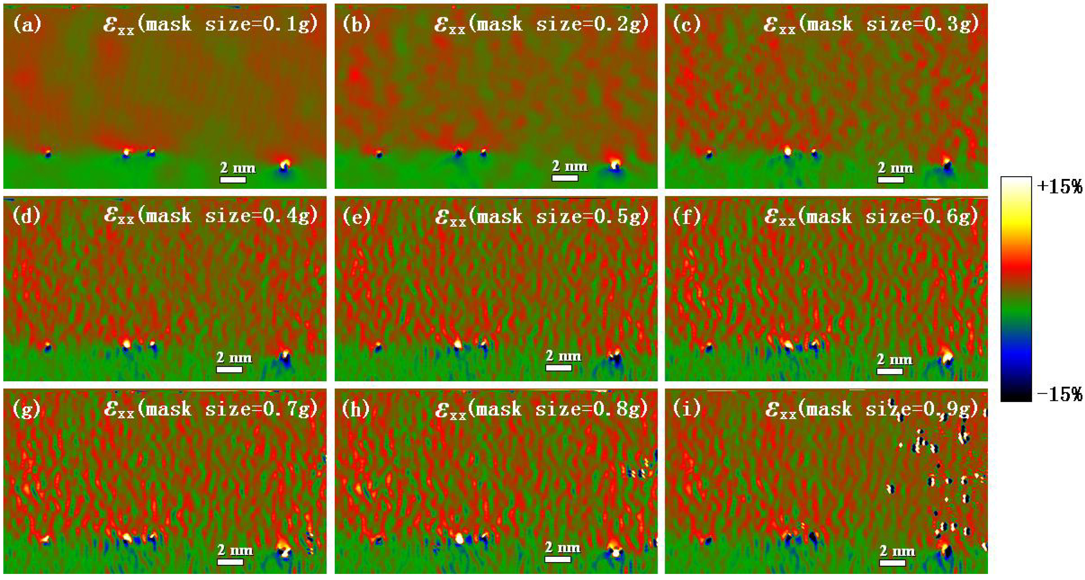
4.3. Effect of Mask Size on the Strain Calculation Results with PPA

4.4. Theoretical Calculation

| a | 1 | 2 | 3 | 4 | 5 | 6 | 7 | 8 | 9 |
|---|---|---|---|---|---|---|---|---|---|
| F(0.1g) | 0.70402 | 0.76388 | 0.82277 | 0.86558 | 0.89697 | 0.92071 | 0.93912 | 0.95377 | 0.96563 |
| F(0.2g) | 0.72084 | 0.78213 | 0.84243 | 0.88626 | 0.91840 | 0.94270 | 0.96155 | 0.97655 | 0.98870 |
| F(0.3g) | 0.80963 | 0.87846 | 0.94619 | 0.99542 | 1.03152 | 1.05881 | 1.07999 | 1.09683 | 1.11048 |
| a | 1 | 2 | 3 | 4 | 5 | 6 | 7 | 8 | 9 |
|---|---|---|---|---|---|---|---|---|---|
| F(0.1g) | 0.81862 | 0.88822 | 0.95670 | 1.00648 | 1.04298 | 1.07058 | 1.09199 | 1.10902 | 1.12282 |
| F(0.2g) | 1.01457 | 1.10084 | 1.18571 | 1.24740 | 1.29264 | 1.32684 | 1.35337 | 1.37449 | 1.39158 |
5. Conclusions
Acknowledgments
References
- Brunner, K. Si/Ge nanostructures. Rep. Prog. Phys. 2002, 65, 27–72. [Google Scholar] [CrossRef]
- Xiang, J.; Lu, W.; Hu, Y.J.; Wu, Y.; Yan, H.; Lieber, C.M. Ge/Si nanowire heterostructures as highperformance field-effect transistors. Nature 2006, 441, 489–493. [Google Scholar] [CrossRef] [PubMed]
- Hu, Y.; Churchill, H.O.; Reilly, D.J.; Xiang, J.; Lieber, C.M.; Marcus, C.M. A Ge/Si heterostructure nanowire-based double quantum dot with integrated charge sensor. Nat. Nanotechnol. 2007, 2, 622–625. [Google Scholar] [CrossRef] [PubMed]
- Park, Y.; Tan, W.; Strachan, A. Strain engineering via amorphization and recrystallization in Si/Ge heterostructures. Phys. Rev. B 2011, 84, 125412:1–125412:7. [Google Scholar]
- Haeni, J.H.; Irvin, P.; Chang, W.; Uecker, R.; Reiche, P.; Li, Y.L.; Choudhury, S.; Tian, W.; Hawley, M.E.; Craigo, B.; et al. Room-temperature ferroelectricity in strained SrTiO3. Nature 2004, 430, 758–761. [Google Scholar] [CrossRef] [PubMed]
- Xu, Z.; Buehler, M.J. Strain controlled reversible thermomutabability in single-walled carbon nanotubes. Nanotechnology 2009, 20, 185701:1–185701:6. [Google Scholar]
- Maeda, Y.; Tsukamoto, N.; Yazawa, Y.; Kanemitsu, Y.; Masumoto, Y. Visible photoluminescence of Ge microcrystals embedded in SiO2 glassy matrices. Appl. Phys. Lett. 1991, 59, 3168–3170. [Google Scholar] [CrossRef] [Green Version]
- Yoshiaki, N.; Kentaro, W.; Yo, F.; Masakazu, I. Observation of the quantum-confinement effect in individual Ge nanocrystals on oxidized Si substrates using scanning tunneling spectroscopy. Appl. Phys. Lett. 2005, 87, 133119:1–133119:3. [Google Scholar]
- Peierls, R.E. The size of a dislocation. Proc. Phys. Soc. Lond. 1940, 52, 34–37. [Google Scholar] [CrossRef]
- Nabarro, F.R.N. Dislocations in a simple cubic lattice. Proc. Phys. Soc. Lond. 1947, 59, 256–272. [Google Scholar] [CrossRef]
- Ren, Q.; Joós, B.; Duesbery, M.S. Test of the Peierls-Nabarro model for dislocations in silicon. Phys. Rev. B 1995, 52, 13223–13228. [Google Scholar] [CrossRef]
- Yao, Y.; Wang, T.; Wang, C. Peierls-Nabarro model of interfacial misfit dislocation: An analytic solution. Phys. Rev. B 1999, 59, 8232–8236. [Google Scholar] [CrossRef]
- Foreman, A.J.; Jaswon, M.A.; Wood, J.K. Factors controlling dislocation widths. Proc. Phys. Soc. Lond. A 1951, 64, 156–163. [Google Scholar] [CrossRef]
- Korsunsky, A.M.; Baimpas, N.; Song, X.; Belnoue, J.; Hofmann, F.; Abbey, B.; Xie, M.; Andrieux, J.; Buslaps, T.; Neo, T.K. Strain tomography of polycrystalline zirconia dental prostheses by synchrotron X-ray diffraction. Acta Mater. 2011, 59, 2501–2513. [Google Scholar] [CrossRef]
- Bierwolf, R.; Hohenstein, M.; Phillipp, F.; Brandt, O.; Crook, G.E.; Ploog, K. Direct measurement of local lattice-distortions in strained layer structures by HREM. Ultramicroscopy 1993, 49, 273–285. [Google Scholar] [CrossRef]
- Rosenauer, A. Transmission Electron. Microscopy of Semiconductor Nanostructures: An Analysis of Composition and Strain, 1st ed.; Springer: Berlin, Germany, 2003; pp. 147–192. [Google Scholar]
- Galindo, P.L.; Kret, S.; Sanchez, A.M.; Laval, J.Y.; Yáñez, A.; Pizarro, J.; Guerrero, E.; Ben, T.; Molina, S.I. The Peak Pairs algorithm for strain mapping from HRTEM images. Ultramicroscopy 2007, 107, 1186–1193. [Google Scholar] [CrossRef] [PubMed]
- Sales, D.L.; Pizarro, J.; Galindo, P.L.; Garcia, R.; Trevisi, G.; Frigeri, P.; Nasi, L.; Franchi, S.; Molina, S.I. Critical strain region evaluation of self-assembled semiconductor quantum dots. Nanotechnology 2007, 18, 475503:1–475503:6. [Google Scholar] [CrossRef]
- Larsson, M.W.; Wagner, J.B.; Wallin, M.; Håkansson, P.; Fröberg, L.E.; Samuelson, L.; Wallenberg, L.R. Strain mapping in free-standing heterostructured wurtzite InAs/InP nanowires. Nanotechnology 2007, 18, 015504:1–015504:8. [Google Scholar] [CrossRef]
- Galindo, P.L.; Pizarro, J.; Molina, S.I.; Ishizuka, K. High resolution peak measurement and strain mapping using peak pairs analysis. Microsc. Anal. 2009, 23, 23–25. [Google Scholar]
- Hÿtch, M.J.; Snoeck, E.; Kilaas, R. Quantitative measurement of displacement and strain fields from HREM micrographs. Ultramicroscopy 1998, 74, 131–146. [Google Scholar] [CrossRef]
- Hÿtch, M.J.; Putaux, J.L.; Pénisson, J.M. Measurement of the displacement field of dislocations to 0.03 Å by electron microscopy. Nature 2003, 423, 270–273. [Google Scholar] [CrossRef] [PubMed]
- Zhao, C.W.; Xing, Y.M.; Zhou, C.E.; Bai, P.C. Experimental examination of displacement and strain fields in an edge dislocation core. Acta Mater. 2008, 56, 2570–2575. [Google Scholar] [CrossRef]
- Johnson, C.L.; Snoeck, E.; Ezcurdia, M.; Rodríguez-González, B.; Pastoriza-Santos, I.; Liz-Marzán, L.M.; Hÿtch, M.J. Effects of elastic anisotropy on strain distributions in decahedral gold nanoparticles. Nat. Mater. 2008, 7, 120–124. [Google Scholar] [CrossRef] [PubMed]
- Liu, Z.W.; Xie, H.M.; Fang, D.N.; Dai, F.L.; Xue, Q.K.; Liu, H. Residual strain around a step edge of artificial Al/Si(111)-7 × 7 nanocluster. Appl. Phys. Lett. 2005, 87, 201908:1–201908:3. [Google Scholar]
- Zhao, C.W.; Xing, Y.M.; Bai, P.C.; Wang, L.F. Quantitative measurement of displacement and strain by the numerical moiré method. Chin. Opt. Lett. 2008, 6, 179–182. [Google Scholar] [CrossRef]
- Su, S.J.; Wang, W.; Cheng, B.W.; Zhang, G.Z.; Hu, W.X.; Xue, C.L.; Zuo, Y.H.; Wang, Q.M. Epitaxial growth and thermal stability of Ge1−xSnx alloys on Ge-buffered Si(001) substrates. J. Cryst. Growth 2011, 317, 43–46. [Google Scholar] [CrossRef]
- Strain Determination Software v2.0. Available online: http://www.uca.es/grup-invest/sic/straintool.htm (accessed on 16 May 2013).
- Hull, D.; Bacon, D.J. Introduction to Dislocations, 5th ed.; Elsevier: Burlington, VT, USA, 2011; pp. 16–19. [Google Scholar]
- Sakai, A.; Tatsumi, T.; Aoyama, K. Growth of strain-relaxed Ge films on Si(001) surfaces. Appl. Phys. Lett. 1997, 71, 3510–3512. [Google Scholar] [CrossRef]
- Kim, T.W.; Lee, D.U.; Lee, H.S.; Lee, J.Y.; Park, H.L. Strain effects and atomic arrangements of 60° and 90° dislocations near the ZnTe/GaAs heterointerface. Appl. Phys. Lett. 2001, 78, 1409–1411. [Google Scholar] [CrossRef]
- Narayan, J. Recent progress in thin film epitaxy across the misfit scale. Acta Mater. 2013, 61, 2703–2724. [Google Scholar] [CrossRef]
- Nakamura, Y.; Murayama, A.; Ichikawa, M. Epitaxial growth of high quality Ge films on Si(001) substrates by nanocontact epitaxy. Cryst. Growth Des. 2011, 11, 3301–3305. [Google Scholar] [CrossRef]
- Hÿtch, M.J.; Houdellier, F.; Hüe, F.; Snoeck, E. Dark-field electron holography for the measurement of geometric phase. Ultramicroscopy 2011, 111, 1328–1337. [Google Scholar] [CrossRef] [PubMed]
- Snedecor, G.W.; Cochran, W.G. Statistical Methods, 8th ed.; Iowa State University Press: Ames, IA, USA, 1989; pp. 73–78. [Google Scholar]
© 2013 by the authors. Licensee MDPI, Basel, Switzerland. This article is an open access article distributed under the terms and conditions of the Creative Commons Attribution license ( http://creativecommons.org/licenses/by/3.0/).
Share and Cite
Li, J.; Zhao, C.; Xing, Y.; Su, S.; Cheng, B. Full-Field Strain Mapping at a Ge/Si Heterostructure Interface. Materials 2013, 6, 2130-2142. https://doi.org/10.3390/ma6062130
Li J, Zhao C, Xing Y, Su S, Cheng B. Full-Field Strain Mapping at a Ge/Si Heterostructure Interface. Materials. 2013; 6(6):2130-2142. https://doi.org/10.3390/ma6062130
Chicago/Turabian StyleLi, Jijun, Chunwang Zhao, Yongming Xing, Shaojian Su, and Buwen Cheng. 2013. "Full-Field Strain Mapping at a Ge/Si Heterostructure Interface" Materials 6, no. 6: 2130-2142. https://doi.org/10.3390/ma6062130