Porous Dielectrics in Microelectronic Wiring Applications

Abstract
:
1. Introduction
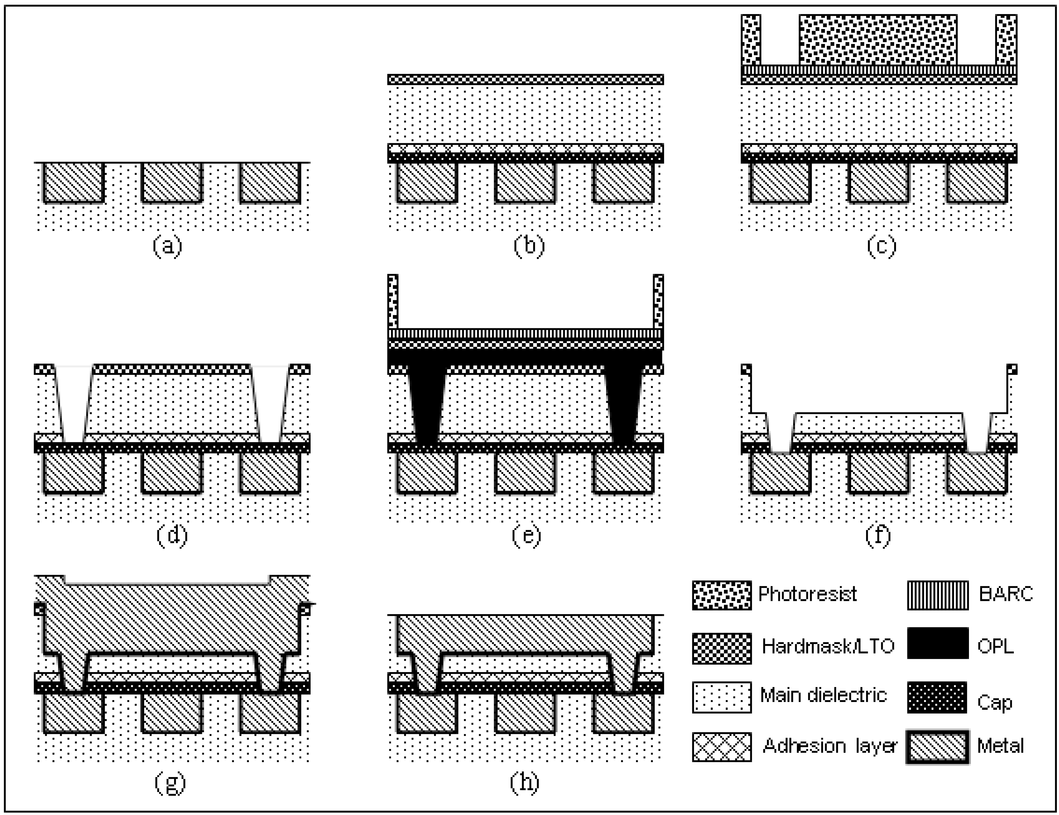
2. Copper Interconnect Fabrication

3. Dielectric Deposition Processes
3.1. Fluorinated SiO2
3.2. Low-K SiCOH
3.3. Ultra Low-K SiCOH
3.4. Spin-on Dielectrics
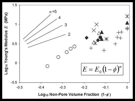
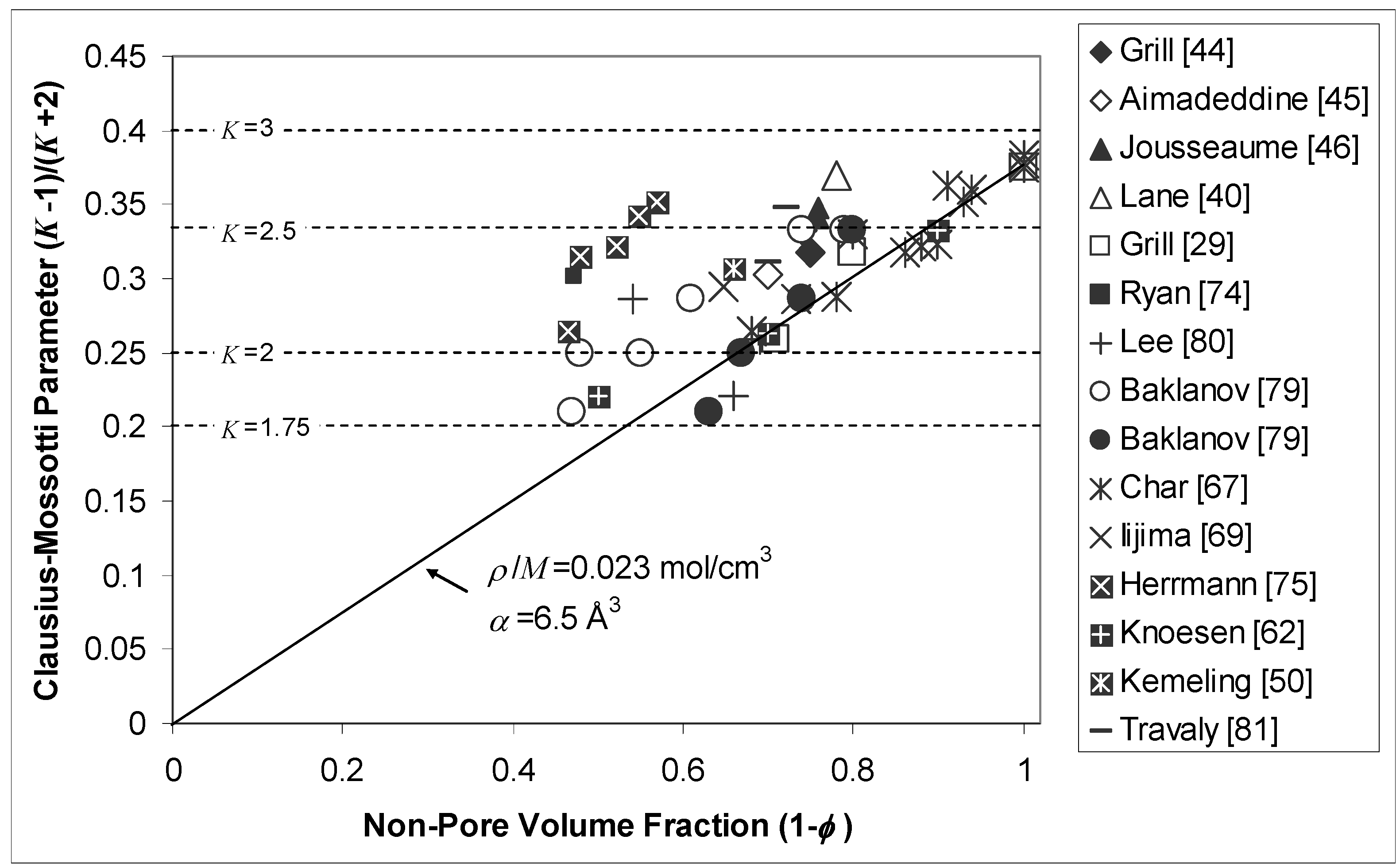
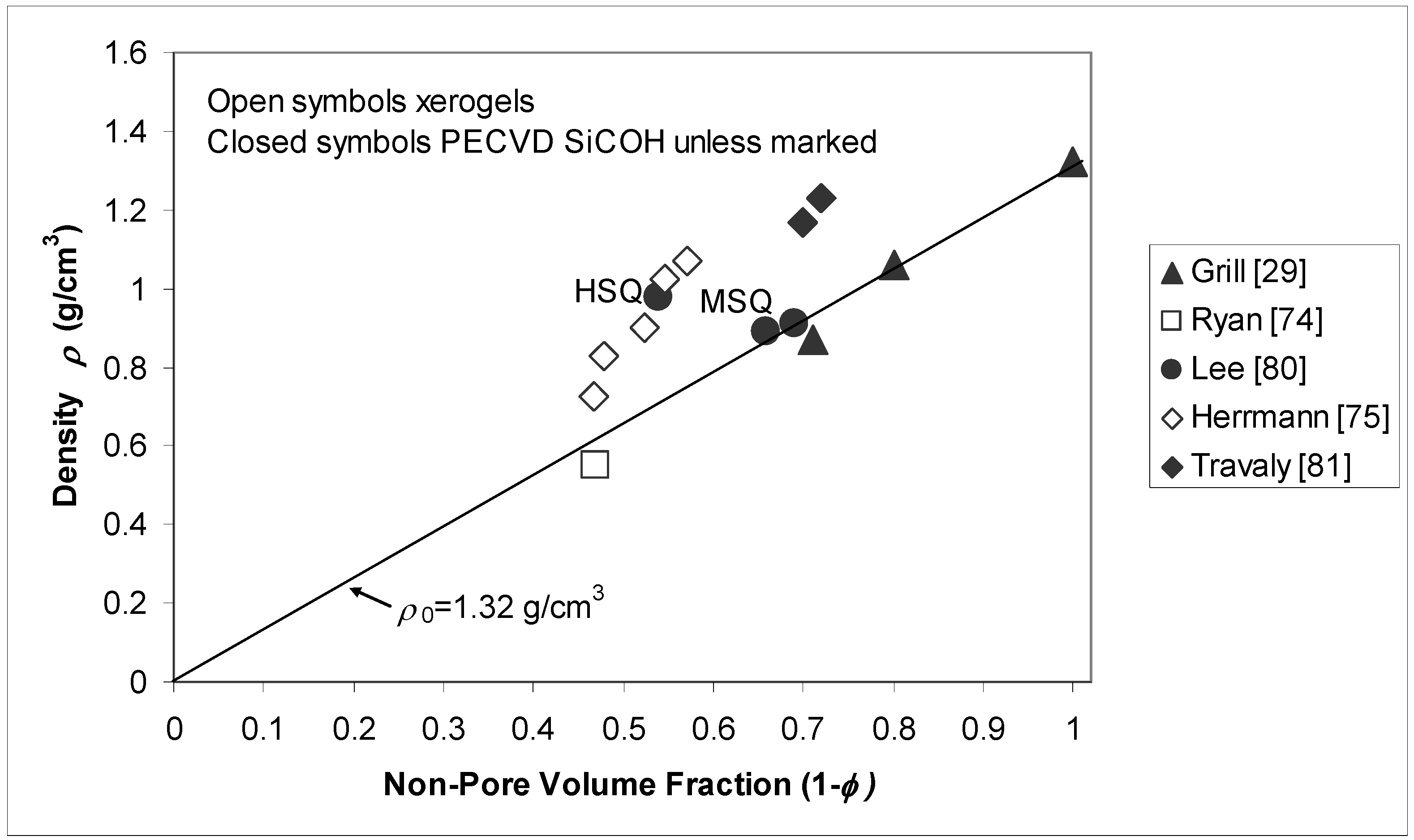
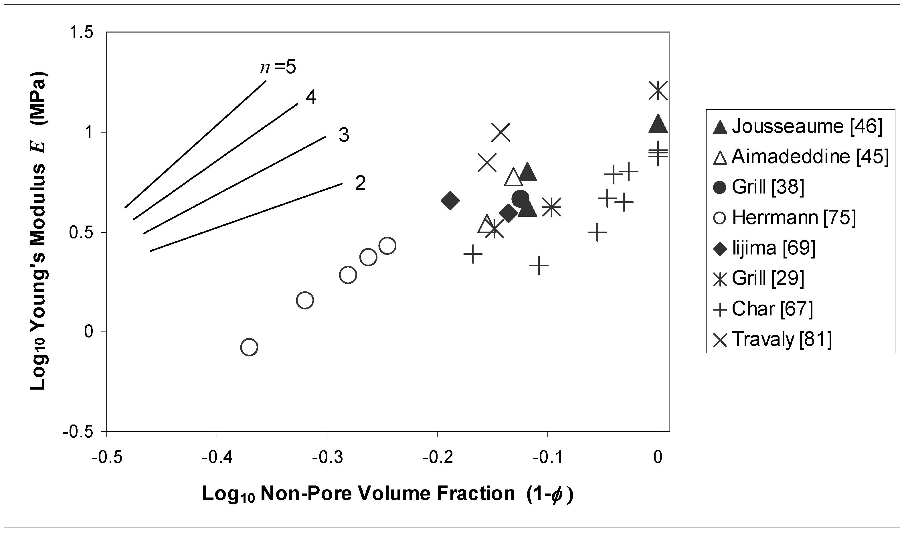
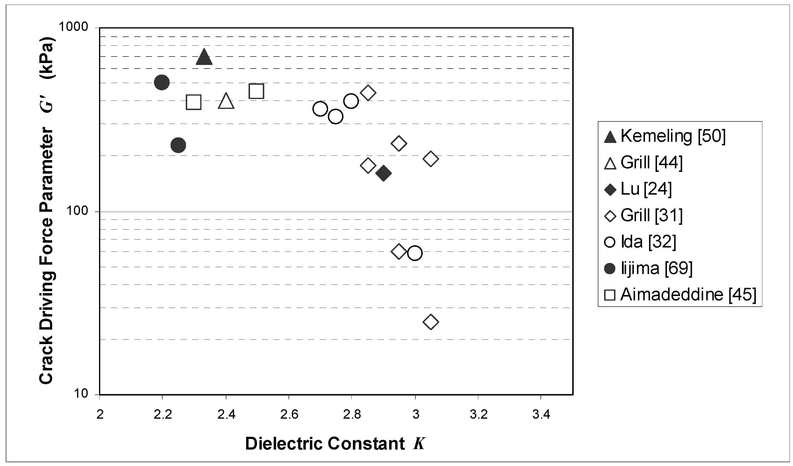
4. Physical Property Trends

5. Plasma-Induced Damage and Repair
6. Concluding Remarks
Acknowledgements
References and Notes
- Taur, Y. CMOS Scaling and Issues in Sub-0.25 um Systems. In Design of High Performance Microprocessor Circuits; Chandrakasan, A., Bowhill, W.J., Fox, F., Eds.; IEEE Press: Piscataway, NJ, USA, 2001; pp. 27–45. [Google Scholar]
- Taur, Y.; Ning, T. Fundamentals of Modern VLSI Devices, 2nd Ed. ed; Cambridge University Press: Cambridge, UK, 2009; pp. 283–289. [Google Scholar]
- Edelstein, D.; Heidenreich, J.; Goldblatt, R.; Cote, W.; Uzoh, C.; Lustig, N.; Roper, P.; McDevitt, T.; Motsiff, W.; Simon, A.; Dukovic, J.; Wachnik, R.; Rathore, H.; Schulz, R.; Su, L.; Luce, S.; Slattery, J. Full Copper Wiring in a Sub-0.25 µm CMOS ULSI Technology. In International Electron Devices Meeting 1997. IEDM Technical Digest (Cat. No.97CH36103); IEEE: New York, NY, USA, 1997; pp. 773–776. [Google Scholar]
- Hu, C.K.; Luther, B. Electromigration in 2-level interconnects of Cu-alloy and Al-alloy. Mater. Chem. Phys. 1995, 41, 1–7. [Google Scholar] [CrossRef]
- Leobandung, E.; Barth, E.; Sherony, M.; Lo, S.-H.; Schulz, R.; Chu, W.; Khare, M.; Sadana, D.; Schepis, D.; Bolam, R.; Sleight, I.; White, F.; Assaderaghi, F.; Moy, D.; Biery, G.; Goldblan, R.; Chen, T.-C.; Davari, B.; Shahidi, G. High performance 0.18 μm SOI CMOS technology. In International Electron Devices Meeting 1999. Technical Digest (Cat. No.99CH36318); IEEE: Piscataway, NJ, USA, 1999; pp. 679–682. [Google Scholar]
- Edelstein, D.; Davis, C.; Clevenger, L.; Yoon, M.; Cowley, A.; Nogami, T.; Rathore, H.; Agarwala, B.; Arai, S.; Carbone, A.; Chanda, K.; Cohen, S.; Cote, W.; Cullinan, M.; Dalton, T.; Das, S.; Davis, P.; Demarest, J.; Dunn, D.; Dziobkowski, C.; Filippi, R.; Fitzsimmons, J.; Flaitz, P.; Gates, S.; Gill, J.; Grill, A.; Hawken, D.; Ida, K.; Klaus, D.; Klymko, N.; Lane, M.; Lane, S.; Lee, J.; Landers, W.; Li, W.-K.; Lin, Y.-H.; Liniger, E.; Liu, X.-H.; Madan, A.; Malhotra, S.; Martin, J.; Molis, S.; Muzzy, C.; Nguyen, D.; Nguyen, S.; Ono, M.; Parks, C.; Questad, D.; Restaino, D.; Sakamoto, A.; Shaw, T.; Shimooka, Y.; Simon, A.; Simonyi, E.; Tempest, S.; Van Kleeck, T.; Vogt, S.; Wang, Y.-Y.; Wille, W.; Wright, J.; Yang, C.-C.; Ivers, T. Reliability, Yield, and Performance of a 90 nm SOI/Cu/SiCOH Technology. In Proceedings of the IEEE 2004 International Interconnect Technology Conference (IEEE Cat. No.04TH8729); IEEE: Piscataway, NJ, USA, 2004; pp. 214–216. [Google Scholar]
- Sankaran, S.; Arai, S.; Augur, R.; Beck, M.; Biery, G.; Bolom, T.; Bonilla, G.; Bravo, O.; Chanda, K.; Chae, M.; Chen, F.; Clevenger, L.; Cohen, S.; Cowley, A.; Davis, P.; Demarest, J.; Doyle, J.; Dimitrakopoulos, C.; Economikos, L.; Edelstein, D.; Farooq, M.; Filippi, R.; Fitzsimmons, J.; Fuller, N.; Gates, S.M.; Greco, S.E.; Grill, A.; Grunow, S.; Hannon, R.; Ida, K.; Jung, D.; Kaltalioglu, E.; Kelling, M.; Ko, T.; Kumar, K.; Labelle, C.; Landis, H.; Lane, M.W.; Landers, W.; Lee, M.; Li, W.; Liniger, E.; Liu, X.; Lloyd, J.R.; Liu, W.; Lustig, N.; Malone, K.; Marokkey, S.; Matusiewicz, G.; McLaughlin, P.S.; McLaughlin, P.V.; Mehta, S.; Melville, I.; Miyata, K.; Moon, B.; Nitta, S.; Nguyen, D.; Nicholson, L.; Nielsen, D.; Ong, P.; Patel, K.; Patel, V.; Park, W.; Pellerin, J.; Ponoth, S.; Petrarca, K.; Rath, D.; Restaino, D.; Rhee, S.; Ryan, E.T.; Shoba, H.; Simon, A.; Simonyi, E.; Shaw, T.M.; Spooner, T.; Standaert, T.; Sucharitaves, J.; Tian, C.; Wendt, H.; Werking, J.; Widodo, J.; Wiggins, L.; Wisnieff, R.; Ivers, T. 45 nm CMOS node Cu/low-k/ ultra low-k PECVD SiCOH (k = 2.4) BEOL technology. In 2006 International Electron Devices Meeting (IEEE Cat No. 06CH37807C); IEEE: Piscataway, NJ, USA, 2006. [Google Scholar]
- Wang, T.C.; Cheng, Y.L.; Wang, Y.L.; Hsieh, T.E.; Hwang, G.J.; Chen, C.F. Comparison of characteristics and integration of copper diffusion-barrier dielectrics. Thin Solid Films 2006, 498, 36–42. [Google Scholar] [CrossRef]
- Grill, A.; Edelstein, D.; Lane, M.; Patel, V.; Gates, S.; Restaino, D.; Molis, S. Interface engineering for high interfacial strength between SiCOH and porous SiCOH interconnect dielectrics and diffusion caps. J. Appl. Phys. 2008, 103, 054104. [Google Scholar] [CrossRef]
- Kriz, J.; Angelkort, C.; Czekalla, M.; Huth, S.; Meinhold, D.; Pohl, A.; Schulte, S.; Thamm, A.; Wallace, S. Overview of dual damascene integration schemes in Cu BEOL integration. Microelectron. Eng. 2008, 85, 2128–2132. [Google Scholar] [CrossRef]
- Fuller, N.C.M.; Worsley, M.A.; Nitta, S.; Dalton, T.; Tai, T.L.; Bent, S.; Magbitang, T.; Dubois, G.; Miller, R.; Volksen, W.; Sankar, M.; Purushothoman, S. Analysis of plasma-induced modification of ULK and eULK materials: dual damascene processing challenges for 45nm (κ < 2.4) and beyond BEOL technologies. In Proceedings of the IEEE 2006 International Interconnect Technology Conference (IEEE Cat. No. 06TH8862C); IEEE: Piscataway, NJ, USA, 2006; pp. 24–26. [Google Scholar]
- Cote, W.; Edelstein, D.; Bunke, C.; Biolsi, P.; Wille, W.; Baks, H.; Conti, R.; Dalton, T.; Houghton, T.; Li, W.-K.; Lin, Y.-H.; Moskowitz, S.; Restaino, D.; Van Kleeck, T.; Vogt, S.; Ivers, T. Non-poisoning dual Damascene patterning scheme for low-k and ultra low-k BEOL. In Advanced Metallization Conference 2006 (AMC 2006). Proceedings; Russell, S.W., Mills, M.E., Osaki, A., Yoda, T., Eds.; Materials Research Society: Warrendale, PA, USA, 2007; pp. 289–294. [Google Scholar]
- Le, Q.T.; Baklanov, M.R.; Kesters, E.; Azioune, A.; Struyf, H.; Boullart, W.; Pireaux, J.J.; Vanhaelemeersch, S. Removal of plasma-modified low-k layer using dilute HF: Influence of concentration. Electrochem. Solid State Lett. 2005, 8, F21–F24. [Google Scholar] [CrossRef]
- Holloway, K.; Fryer, P.M.; Cabral, C.; Harper, J.M.E.; Bailey, P.J.; Kelleher, K.H. Tantalum as a diffusion barrier between copper and silicon – failure mechanism and effect of nitrogen additions. J. Appl. Phys. 1992, 71, 5433–5444. [Google Scholar] [CrossRef]
- Lloyd, J.R.; Ponoth, S.; Liniger, E.; Cohen, S. Role of Cu in TDDB of low-k dielectrics. In 2007 IEEE International Reliability Physics Symposium Proceedings (IEEE Cat. No.07CH37867); IEEE: Piscataway, NJ, USA, 2007. [Google Scholar]
- Liu, X.H.; Shaw, T.M.; Lane, M.W.; Rosenberg, R.R.; Lane, S.L.; Doyle, J.P.; Restaino, D.; Vogt, S.F.; Edelstein, D.C. Channel cracking in low-k film son patterned multilayers. In Proceedings of the IEEE 2004 International Interconnect Technology Conference; IEEE: Piscataway, NJ, USA, 2004; pp. 93–95. [Google Scholar]
- Cote, D.R.; Nguyen, S.V.; Stamper, A.K.; Armbrust, D.S.; Tobben, D.; Conti, R.A.; Lee, G.Y. Plasma-assisted chemical vapor deposition of dielectric thin films for ULSI semiconductor circuits. IBM J. Res. Develop. 1999, 43, 5–31. [Google Scholar] [CrossRef]
- Nguyen, S.V. High-density plasma chemical vapor deposition of silicon-based dielectric films for integrated circuits. IBM J. Res. Develop. 1999, 43, 109–126. [Google Scholar] [CrossRef]
- Shapiro, M.J.; Nguyen, S.V.; Matsuda, T.; Dobuzinsky, D. CVD of fluorosilicate glass for ULSI applications. Thin Solid Films 1995, 270, 503–507. [Google Scholar] [CrossRef]
- Sikder, A.K.; Kumar, A.; Thagella, S.; Yota, J. Effects of properties and growth parameters of doped and undoped silicon oxide films on wear behavior during chemical mechanical planarization process. J. Mater. Res 2004, 19, 996–1010. [Google Scholar] [CrossRef]
- Oshima, T.; Tamaru, T.; Ohmori, K.; Aoki, H.; Ahihara, H.; Saito, T.; Yamaguchi, H.; Miyauchi, M.; Torii, K.; Murata, J.; Satoh, A.; Miyazaki, H.; Hinode, K. Improvement of thermal stability of via resistance in dual damascene copper interconnection. In International Electron Devices Meeting 2000. Technical Digest. IEDM (Cat. No.00CH37138); IEEE: Piscataway, NJ, USA, 2000; pp. 123–126. [Google Scholar]
- Grill, A.; Patel, V. Low dielectric constant films prepared by plasma-enhanced chemical vapor deposition from tetramethylsilane. J. Appl. Phys. 1999, 85, 3314–3318. [Google Scholar] [CrossRef]
- Loboda, M.J. New solutions for intermetal dielectrics using trimethylsilane-based PECVD processes. Microelectron. Eng. 2000, 50, 15–23. [Google Scholar] [CrossRef]
- Lu, J.C.; Chang, W.; Jang, S.M.; Yu, C.H.; Liang, M.S. Development of 300mm low K dielectric for 0.13 um BEOL damascene process. In Proceedings of the IEEE 2004 International Interconnect Technology Conference (IEEE Cat. No.04TH8729); IEEE: Piscataway, NJ, USA, 2004; pp. 63–65. [Google Scholar]
- Shamiryan, D.; Weidner, K.; Gray, W.D.; Baklanov, M.R.; Vanhaelemeersch, S.; Maex, K. Comparative study of PECVD SiCOH low-k films obtained at different deposition conditions. Microelectron. Eng. 2002, 64, 361–366. [Google Scholar] [CrossRef]
- Cheng, Y.L.; Wang, Y.L.; Hwang, G.J.; Lee, W.H.; O'Neill, M.L.; Tang, A.; Wu, C.L. Optimization and integration of trimethylsilane-based organosilicate glass and organofluorinated silicate glass dielectric thin films for Cu damascene process. J. Vac. Sci. Technol. B 2007, 25, 96–101. [Google Scholar] [CrossRef]
- Grill, A.; Perraud, L.; Patel, V.; Jahnes, C.; Cohen, S. Low dielectric constant SiCOH films as potential candidates for interconnect dielectrics. In Low-Dielectric Constant Materials V. Proceedings (Materials Research Society Symposium Proceedings); Materials Research Society: Warrendale, PA, USA, 1999; Volume 565, pp. 107–116. [Google Scholar]
- Rouessac, V.; Favennec, L.; Remiat, B.; Jousseaume, V.; Passernard, G.; Durand, J. Precursor chemistry for ULK CVD. Microelectron. Eng. 2005, 82, 333–340. [Google Scholar]
- Grill, A. Plasma enhanced chemical vapor deposited SiCOH dielectrics: from low-k to extreme low-k interconnect materials. J. Appl. Phys. 2003, 93, 1785–1790. [Google Scholar] [CrossRef]
- Lin, Y.; Tsui, T.Y.; Vlassak, J.J. Octomethylcyclotetrasiloxane-based, low-permittivity organosilicate coatings. J. Electrochem. Soc. 2006, 153, F144–F152. [Google Scholar] [CrossRef]
- Grill, A.; Edelstein, D.; Restaino, D.; Lane, M.; Gates, S.; Liniger, E.; Shaw, T.; Liu, X.H.; Klaus, D.; Patel, V.; Cohen, S.; Simonyi, E.; Klymko, N.; Lane, S.; Ida, K.; Vogt, S.; Van Kleeck, T.; Davis, C.; Ono, M.; Nogami, T.; Ivers, T. Optimization of SiCOH dielectrics for integration in a 90 nm CMOS technology. In Proceedings of the IEEE 2004 International Interconnect Technology Conference (IEEE Cat. No.04TH8729); IEEE: Piscataway, NJ, USA, 2004; pp. 54–56. [Google Scholar]
- Ida, K.; Nguyen, S.; Lane, S.; Klymko, N.; Chanda, K.; Chen, F.; Christiansen, C.; Cohen, S.; Cullinan, M.; Dziobkowski, C.; Flaitz, P.; Fitzsimmons, J.; Fukasawa, M.; Gill, J.; Grill, A.; Inoue, K.; Kumar, K.; Labelle, C.; Lane, M.; Liniger, E.; Madon, A.; Malone, K.; Martin, J.; McGahay, V.; Minami, M.; Molis, S.; Restaino, D.; Sakamoto, A.; Sankar, M.; Sherwood, M.; Simonyi, E.; Shimooka, Y.; Tai, L.; Widodo, J.; Wildman, H.; Ono, M.; McHerron, D.; Nye, H.; Edelstein, D.; Nogami, T.; Ivers, T. PECVD low-k (~2.7) dielectric SiCOH film development and integration for 65nm CMOS devices. In Advanced Metallization Conference 2005 (AMC 2005). Proceedings of the Conference; Brongersma, S.H., Taylor, T.C., Tsujimura, M., Masu, K., Eds.; Materials Research Society: Warrendale, PA, USA, 2006; pp. 85–96. [Google Scholar]
- Prager, L.; Marsik, P.; Wennrich, L.; Baklanov, M.R.; Naumov, S.; Pistol, L.; Schneider, D.; Gerlach, J.W.; Verdonck, P.; Buchmeiser, M.R. Effect of pressure on efficiency of UV curing of CVD-derived low-k material at different wavelengths. Microelectron. Eng. 2008, 85, 2094–2097. [Google Scholar] [CrossRef]
- Gage, D.M.; Guyer, E.P.; Stebbins, J.F.; Cui, Z.; Al-Bayati, A.; Demos, A.; MacWilliams, K.P.; Dauskardt, R.H. UV curing effects on glass structure and mechanical properties of organosilicate low-k thin films. In Proceedings of the IEEE 2006 International Interconnect Technology Conference (IEEE Cat. No. 06TH8862C); IEEE: Piscataway, NJ, USA, 2006; pp. 149–151. [Google Scholar]
- Chapelon, L.L.; Vitiello, J.; Gonchond, J.P.; Barbier, D.; Torres, J. UV curing effects on mechanical and electrical performance of a PECVD non-porogen SiOC:H films (in k [2.2–2.4] range) for 45nm node and below. Microelectron. Eng. 2006, 83, 2136–2141. [Google Scholar] [CrossRef]
- Tajima, N.; Ohno, T.; Hamada, T.; Yoneda, K.; Kobayashi, N.; Shinriki, M.; Miyazawa, K.; Sakota, K.; Hasaka, S.; Inoue, M. Carbon-rich SiCOH films with hydrocarbon network bonds for low-k dielectrics: first-principles investigation. In Proceedings of the IEEE 2006 International Interconnect Technology Conference (IEEE Cat. No. 06TH8862C); IEEE: Piscataway, NJ, USA, 2006; pp. 122–124. [Google Scholar]
- Tajima, N.; Ohashi, Y.; Nagano, S.; Xu, Y.; Matsumoto, S.; Kada, T.; Ohno, T. Theoretical analyses of chemical reactions for forming hydrocarbon-bridged SiCOH low-K films in PECVD processes. In 2009 IEEE International Interconnect Technology Conference–IITC; IEEE: Piscataway, NJ, USA, 2009; pp. 116–118. [Google Scholar]
- Grill, A.; Patel, V.; Rodbell, K.P.; Huang, E.; Baklanov, M.R.; Mogilnikov, K.P.; Toney, M.; Kim, H.C. Porosity in plasma enhanced chemical vapor deposited SiCOH dielectrics: a comparative study. J. Appl. Phys. 2003, 94, 3427–3435. [Google Scholar] [CrossRef]
- Shaw, T.M.; Jimerson, D.; Haders, D.; Murray, C.E.; Grill, A.; Edelstein, D.C.; Chidambarrao, D. Moisture and oxygen uptake in low k/copper interconnect structures. In Advanced Metallization Conference 2003 (AMC 2003); Ray, G.W., Smy, T., Ohla, T., Tsujimura, M., Eds.; Materials Research Society: Warrendale, PA, USA, 2004; pp. 77–84. [Google Scholar]
- Lane, S.; Fukusawa, M.; Angyal, M.; Chanda, K.; Chen, F.; Christiansen, C.; Fitzsimmons, J.; Gill, J.; Ida, K.; Inoue, K.; Kumar, K.; Li, B.; McLaughlin, P.; Melville, I.; Nimami, M.; Nguyen, S.; Penny, C.; Sakamoto, A.; Shimooka, Y.; Ono, M.; McHerron, D.; Nogami, T.; Ivers, T. BEOL process integration with Cu/SiCOH (k = 2.8) low-k interconnects at 65nm groundrules. In Advanced Metallization Conference 2005 (AMC 2005). Proceedings of the Conference; Brongersma, S.H., Taylor, T.C., Tsujimura, M., Masu, K., Eds.; Materials Research Society: Warrendale, PA, USA, 2006; pp. 61–71. [Google Scholar]
- Grill, A.; Patel, V. Ultralow-k dielectrics prepared by plasma-enhanced chemical vapor deposition. Appl. Phys. Lett. 2001, 79, 803–805. [Google Scholar] [CrossRef]
- Grill, A.; Patel, V. Ultralow dielectric constant pSiCOH films prepared tetramethylcyclo-tetrasiloxane as skeleton precursor. J. Appl. Phys. 2008, 104, 024113:1–024113:9. [Google Scholar] [CrossRef]
- Gates, S.M.; Neumayer, D. A.; Sherwood, M. H.; Grill, A.; Wang, X.; Sankarapandian, M. Preparation and structure of porous dielectrics by plasma enhanced chemical vapor deposition. J. Appl. Phys. 2007, 101, 094103:1–094103:8. [Google Scholar] [CrossRef]
- Grill, A.; Gates, S.; Dimitrakopoulos, C.; Pagel, V.; Cohen, S.; Ostrovski, Y.; Liniger, E.; Simonyi, E.; Restaino, D.; Sankaran, S.; Reiter, S.; Demos, A.; Yim, K.S.; Nguyen, V.; Rocha, J.; Ho, D. Development and optimization of porous pSiCOH interconnect dielectrics for 45 nm and beyond. In Proceedings of the IEEE 2008 International Interconnect Technology Conference; IEEE: Piscataway, NJ, USA, 2008; pp. 28–30. [Google Scholar]
- Aimadeddine, M.; Jousseaume, V.; Amal, V.; Favennec, L.; Farcy, A.; Zenasni, A.; Assous, M.; Vilmay, M.; Jullian, S.; Maury, P.; Delaye, V.; Jourdan, N.; Vanypre, T.; Brun, P.; Imbert, G.; LeFriec, Y.; Mellier, M.; Chaabouni, H.; Chapelon, L.L.; Hamioud, K.; Volpi, F.; Louis, D.; Passemard, G.; Torres, J. Robust integration of an ULK SiOCH dielectric (k = 2.3) for high performance 32 nm node BEOL. In 2007 10th International Interconnect Technology Conference; IEEE: Piscataway, NJ, USA, 2007; pp. 175–177. [Google Scholar]
- Jousseaume, V.; Zenasni, A.; Favennec, L.; Gerbaud, G.; Bardet, M.; Simon, J.P.; Humbert, A. Comparison between e-beam and ultraviolet curing to perform porous a-SiOC:H. J. Electrochem. Soc. 2007, 154, G103–G109. [Google Scholar] [CrossRef]
- Burkey, D.D.; Gleason, K.K. Temperature-resolved Fourier transform infrared study of condensation reactions and porogen decomposition in hybrid organosilicon porogen films. J. Vac. Sci. Technol. A 2004, 22, 61–70. [Google Scholar] [CrossRef]
- Favennec, L.; Jousseaume, V.; Gerbaud, G.; Zenasni, A.; Passemard, G. Ultralow k using a plasma enhanced chemical vapor deposition porogen approach: matrix structure and porogen loading influences. J. Appl. Phys. 2007, 102, 064107:1–064107:9. [Google Scholar] [CrossRef]
- Castex, A.; Jousseaume, V.; Deval, J.; Bruat, J.; Favennec, L.; Passemard, G. Ultralow k using a plasma-enhanced chemical vapor deposition porogen approach: study of the precursor reaction mechanisms. J. Vac. Sci. Technol. A 2008, 26, 1343–1354. [Google Scholar] [CrossRef]
- Kemeling, N.; Matsushita, K.; Tsuji, N.; Kagami, K.; Kato, M.; Kaneko, S.; Sprey, H.; de Roest, D.; Kobayashi, N. A robust k~2.3 SiCOH low-k film formed by porogen removal with UV-cure. Microelectron. Eng. 2007, 84, 2575–2581. [Google Scholar] [CrossRef]
- Nakao, S.-I.; Ushio, J.; Ohno, T.; Hamada, T.; Kamigaki, Y.; Kato, M.; Yoneda, K.; Kondo, S.; Kobayashi, N. UV/EB cure mechanism for porous PECVD/SOD low-k SiCOH materials. In Proceedings of the IEEE 2006 International Interconnect Technology Conference (IEEE Cat. No. 06TH8862C); IEEE: Piscataway, NJ, USA, 2006; pp. 66–68. [Google Scholar]
- Seo, K.; Oka, Y.; Nomura, K.; Tsutsue, M.; Kobori, E.; Goto, K.; Mizukami, Y.; Ohtsuka, T.; Tsukamoto, K.; Matsumoto, S.; Ueda, T. New multi-step UV curing process for porogen-based porous SiOC. In 2009 IEEE International Interconnect Technology Conference – IITC; IEEE: Piscataway, NJ, USA, 2009; pp. 101–103. [Google Scholar]
- Owada, T.; Ohara, N.; Watatani, H.; Kouno, T.; Kudo, H.; Ochimizu, H.; Sakoda, T.; Asami, N.; Ohkura, Y.; Fukuyama, S.; Tsukune, A.; Nakaishi, M.; Nakamura, T.; Nara, Y.; Kase, M. Advanced BEOL integration using porous low-k (k = 2.25) material with charge-damage-less electron beam cure technique. In 2009 IEEE International Interconnect Technology Conference – IITC; IEEE: Piscataway, NJ, USA, 2009; pp. 149–151. [Google Scholar]
- Kwak, S.-K.; Jeong, K.H.; Rhee, S.W. Nanocomposite low-k SiCOH films by direct PECVD using vinyltrimethylsilane. J. Electrochem. Soc. 2004, 151, F11–F16. [Google Scholar] [CrossRef]
- Asami, N.; Owada, T.; Akiyama, S.; Ohara, N.; Iba, Y.; Kouno, T.; Kudo, H.; Takesako, S.; Osada, T.; Kirimura, T.; Watatani, H.; Uedono, A.; Nara, Y.; Kase, M. Novel low-k SiOC (k = 2.4) with superior tolerance to direct polish and ashing for advanced BEOL integration. In 2009 IEEE International Interconnect Technology Conference – IITC; IEEE: Piscataway, NJ, USA, 2009; pp. 161–162. [Google Scholar]
- Burkey, D.D.; Gleason, K.K. Organosilicon thin films deposited from cyclic and acyclic precursors using water as an oxidant. J. Electrochem. Soc. 2004, 151, F105–F112. [Google Scholar] [CrossRef]
- Tada, M.; Yamamoto, H.; Ito, F.; Takeuchi, T.; Furutake, N.; Hayashi, Y. Chemical structure effects of ring-type siloxane precursors on properties of plasma-polymerized porous SiCOH films. J. Electrochem. Soc. 2005, 154, D354–D361. [Google Scholar] [CrossRef]
- Yasuhara, S.; Chung, J.; Tajima, K.; Yano, H.; Kadomura, S.; Yoshimaru, M.; Matsunaga, N.; Kubota, T.; Ohtake, H.; Samukawa, S. Structure-designable method to form super low-k SiOC film (k = 2.2) by neutral-beam-enhanced chemical vapour deposition. J. Phys. D–Appl. Phys. 2009, 42, 055208:1–055208:7. [Google Scholar]
- Grill, A. Porous pSiCOH ultralow-k dielectrics for chip interconnects prepared by PECVD. Annu. Rev. Mater. Res. 2009, 39, 49–69. [Google Scholar] [CrossRef]
- Pineda, R.; Chiang, C.; Fraser, D.B. A new caged structure spin-on silica for multilevel interconnect application. In 1990 Proceedings. Seventh International IEEE VLSI Multilevel Interconnection Conference (Cat. No.90TH0325–1); IEEE: New York, NY, USA, 1990; pp. 180–186. [Google Scholar]
- McGahay, V.; Acovic, A.; Agarwala, B.; Endicott, G.; Nguyen, D.; Shapiro, M.; Yankee, S. Process integration and reliability of hydrogen silsesquioxane in direct-on-metal application. In 1996 Proceedings Thirteenth International VLSI Multilevel Interconnection Conference (VMIC); VMIC: Tampa, FL, USA; pp. 116–118.
- Knoesen, A.; Song, G.; Volksen, W.; Huang, E.; Magbitang, T.; Sundberg, L.; Hedrick, J.L.; Hawker, C.J.; Miller, R.D. Porous organosilicates low-dielectric films for high frequency devices. J. Electron. Mater. 2004, 33, 135–140. [Google Scholar] [CrossRef]
- Lazzeri, P.; Vanzetti, L.; Anderle, M.; Bersani, M.; Park, J.J.; Lin, Z.; Briber, R.M.; Rubloff, G.W.; Kim, H.C.; Miller, R.D. Thin-film transformations and volatile products in the formation of nanoporous low-k polymethylsilsesqioxane-based dielectric. J. Vac. Sci. Technol. B 2005, 23, 908–917. [Google Scholar] [CrossRef]
- Padovani, A.M.; Rhodes, L.; Allen, S.A.B.; Kohl, P.A. Chemically bonded porogens in methylsilsesquioxane I. Structure and bonding. J. Electrochem. Soc. 2002, 149, F161–F170. [Google Scholar] [CrossRef]
- Padovani, A.M.; Riester, L.K.; Rhodes, L.; Allen, S.A.B.; Kohl, P.A. Chemically bonded porogens in methylsilsesquioxane II. Electrical, optical, and mechanical properties. J. Electrochem. Soc. 2002, 149, F171–F180. [Google Scholar] [CrossRef]
- Peng, H.-G.; Vallery, R.S.; Liu, M.; Frieze, W.E.; Gidley, D.W.; Yim, J.-H.; Kim, J. Deducing nonopore structure and growth mechanisms in porogen-templated silsesquioxane thin films. Appl. Phys. Lett. 2005, 87, 161903:1–161903:3. [Google Scholar]
- Char, K.; Cha, B.J.; Kim, S. Material issues for nanoporous ultra low-k dielectrics. In Proceedings of the IEEE 2004 International Interconnect Technology Conference (IEEE Cat. No.04TH8729); IEEE: Piscataway, NJ, USA, 2004; pp. 219–221. [Google Scholar]
- Lin, C.-F.; Tung, I-C.; Feng, M.-S. Effects of methyl silsesquioxane electron-beam curing on device characteristics of logic and four-transistor static random-access memory. Jpn. J. Appl. Phys. Pt. 1 1999, 38, 6253–6257. [Google Scholar]
- Iijima, T.; Lin, Q.; Chen, S.; Labelle, C.; Fuller, N.; Ponoth, S.; Cohen, S.; Lloyd, J.; Dunn, D.; Muzzy, C.; Gill, J.; Nitta, S.; McGahay, V.; Tyberg, C.; Spooner, T.; Nye, H. BEOL integration of highly damage-resistant porous ultra low-K material using direct CMP and via-first process. In Proceedings of the IEEE 2006 International Interconnect Technology Conference (IEEE Cat. No. 06TH8862C); IEEE: Piscataway, NJ, USA, 2006; pp. 21–23. [Google Scholar]
- Volksen, W.; Dubois, G.; Kellock, A.; Magbitang, T.P.; Miller, R.D.; Cohen, S.; Simonyi, E.; Ramirez, L.; Wang, Y. Laser spike annealing: a novel post-porosity treatment for significant toughening of low-k organosilicates. In Proceedings of the IEEE 2006 International Interconnect Technology Conference (IEEE Cat. No. 06TH8862C); IEEE: Piscataway, NJ, USA, 2006; pp. 146–148. [Google Scholar]
- Wang, P.-I.; Wu, Z.; Lu, T.-M.; Interrante, L. A novel polycarbosilane-based low-k dielectric material. J. Electrochem. Soc. 2006, 153, G267–G271. [Google Scholar] [CrossRef]
- Yamazaki, T.; Hirakawa, M.; Nakayama, T.; Murakami, H. Development of porous silica ultra low-k films for 32nm-node interconnects and beyond. In 2009 IEEE International Interconnect Technology Conference – IITC; IEEE: Piscataway, NJ, USA, 2009; pp. 119–121. [Google Scholar]
- Nitta, S.V.; Pisupatti, V.; Jain, A.; Wayner, P.C.; Gill, W.N.; Plawsky, J.L. Surface modified spin-on xerogel films as interlayer dielectrics. J. Vac. Soc. Technol. B 1999, 17, 205–212. [Google Scholar] [CrossRef]
- Ryan, E.T.; Ho, H.-M.; Wu, W.-L.; Ho, P.S.; Gidley, D.W.; Drage, J. Material property characterization and integration issues for mesoporous silica. In Proceedings of the IEEE 1999 International Interconnect Technology Conference (Cat. No.99EX247); IEEE: Piscataway, NJ, USA, 1999; pp. 197–189. [Google Scholar]
- Herrmann, M.; Richter, F.; Schulz, S.E. Study of nano-mechanical properties for thin porous films through instrumented indentation: SiO2 low dielectric constant films as an example. Microelectron. Eng. 2008, 85, 2172–2174. [Google Scholar] [CrossRef]
- Goldblatt, R.D.; Agarwala, B.; Anand, M.B.; Barth, E.P.; Biery, G.A.; Chen, Z.G.; Cohen, S.; Connolly, J.B.; Cowley, A.; Dalton, T.; Das, S.K.; Davis, C.R.; Deutsch, A.; DeWan, C.; Edelstein, D.C.; Emmi, P.A.; Faltermeier, C.G.; Fitzsimmons, J.A.; Hedrick, J.; Heidenreich, J.E.; Hu, C.K.; Hummel, J.P.; Jones, P.; Kaltalioglu, E.; Kastenmeier, B.E.; Krishnan, M.; Landers, W.F.; Liniger, E.; Liu, J.; Lustig, N.E.; Malhotra, S.; Manger, D.K.; McGahay, V.; Mih, R.; Nye, H.A.; Purushothaman, S.; Rathore, H.A.; Seo, S.C.; Shaw, T.M.; Simon, A.H.; Spooner, T.A.; Stetter, M.; Wachnik, R.A.; Ryan, J.G. A high performance 0.13 μm copper BEOL technology with low-k dielectric. In Proceedings of the IEEE 2000 International Interconnect Technology Conference (Cat. No.00EX407); IEEE: Piscataway, NJ, USA, 2000; pp. 261–263. [Google Scholar]
- McGahay, V.; Adams, C.; Barth, E.; Biery, G.; Chen, Z.; Chen, X.; Das, S.; Davis, C.; Engel, B.; Fitzsimmons, J.; Gill, J.; Gambino, J.; Geffken, R.; Goldblatt, R.; Hadel, L.; Kastenmeier, B.; Klaasen, W.; Landers, W.; Luce, S.; Lustig, N.; Marino, J.; Martin, A.; McDevitt, T.; McGrath, J.; Melville, I.; Nguyen, D.; Procter, R.; Rathore, H.; Seo, S.-C.; Spooner, T.; Stamper, A.; Standaert, T.; Tian, C.; Wynne, J. Cu/SiLK integration: influence of process on reliability. In Advanced Metallization Conference 2001 (AMC 2001). Proceedings of the Conference; McKerrow, A.J., Shacham-Diamand, Y., Zaima, S., Ohba, T., Eds.; Materials Research Society: Warrendale, PA, USA, 2001; pp. 3–9. [Google Scholar]
- Strittmatter, R.J.; Hahnfeld, J.L.; Silvis, H.C.; Stokich, T.M.; Perry, J.D.; Ouellette, K.B.; Niu, Q.J.; Godschalx, J.P.; Kalantar, T.H.; Mubarekyan, E.; Hefner, R.E., Jr.; Lyons, J.W.; Dominowski, J.M.; Buske, G.R. Development of porous SiLK trade semiconductor dielectric resin for the 65 nm and 45 nm nodes. In Materials, Technology and Reliability for Advanced Interconnects and Low-k Dielectrics - Symposium 2003; McKerrow, A.J., Leu, J., Kraft, O., Kikkawa, T., Eds.; Materials Research Society: Warrendale, PA, USA, 2003; pp. 265–272. [Google Scholar]
- Baklanov, M.R.; Mogilnikov, K.P. Non-destructive characterization of low-k dielectric films. Microelectron. Eng. 2002, 64, 335–349. [Google Scholar] [CrossRef]
- Lee, H.-J.; Soles, C.L.; Liu, D.-W.; Bauer, B.J.; Lin, E.K.; Grill, A. Structural characterization of porous low-k thin films prepared by different techniques using X-ray porosimetry. J. Appl. Phys. 2004, 95, 2355–2359. [Google Scholar] [CrossRef]
- Travaly, Y.; Sinapi, F.; Heylen, N.; Humbert, A.; Delande, M.; Caluwaert, R.; de Mussy, J.P.; Vereecke, G.; Baklanov, M.R.; Iacopi, F.; Hernandez, J.L.; Beyer, G.; Fischer, P. The critical role of the metal/porous low-k interface in post direct CMP defectivity generation and resulting ULK surface and bulk hydrophilisation. In 2007 10th International Interconnect Technology Conference; IEEE: Piscataway, NJ, USA, 2007; pp. 164–167. [Google Scholar]
- Bruggeman, D.A.G. Berechnung verschiedener physikalischer Konstanten von heterogenen Substanzen. I. Dielektrizitatskonstanten und Leitfahigkeiten der Mischkorper aus isotropen Substanzen. Annalen der Physik (Leipzig) 1935, 24, 636–664. [Google Scholar] [CrossRef]
- Wagh, A.S.; Poeppel, R.B.; Singh, J.P. Open pore description of mechanical properties of ceramics. J. Mater. Sci. 1991, 26, 3862–3868. [Google Scholar] [CrossRef]
- Munro, R.G. Analytical representations of elastic moduli data with simultaneous dependence on temperature and porosity. J. Res. NIST 2004, 109, 497–503. [Google Scholar] [CrossRef]
- Liniger, E.G.; Simonyi, E.E. Moisture-driven crack growth in blanket low dielectric constant and ultralow dielectric constant films. J. Appl. Phys. 2004, 96, 3482–3485. [Google Scholar]
- Lane, M.W.; Liu, X.H.; Shaw, T.M. Environmental effects on cracking and delamination of dielectric films. IEEE Trans. Device Mater. Reliability 2004, 4, 142–146. [Google Scholar] [CrossRef]
- Ryan, E.T.; Martin, H.; Junker, K.; Wetzel, J. Effect of material properties on intgeration damage in organosilicate films. J. Mater. Res. 2001, 16, 3335–3338. [Google Scholar] [CrossRef]
- Worsley, M.A.; Roberts, M.; Bent, S.F.; Gates, S.M.; Shaw, T.; Volksen, W.; Miller, R. Detection of open or closed porosity in low-κ dielectrics by solvent diffusion. Microelectron. Eng. 2005, 82, 113–118. [Google Scholar] [CrossRef]
- Kagawa, Y.; Enomoto, Y.; Kameshima, T.; Okomoto, M.; Kawashima, H.; Yamada, A.; Hasegawa, T.; Akiyama, K.; Masuda, H.; Miyajima, H.; Shibata, H.; Kadomura, S. Robust 45nm node Cu/ULK interconnects using effective porogen control. In Proceedings of the IEEE 2006 International Interconnect Technology Conference (IEEE Cat. No. 06TH8862C); IEEE: Piscataway, NJ, USA, 2006; pp. 207–210. [Google Scholar]
- Caluwaerts, R.; Van Hove, M.; Beyer, G.; Hoofman, R.J.O.M.; Struyf, H.; Verheyden, G.J.A.M.; Waeterloos, J.; Tokei, Zs.; Iacopi, F.; Carbonell, L.; Le, Q.T.; Das, A.; Vos, I.; Demuynck, S.; Maex, K. Post patterning meso porosity creation: a potential solution for pore sealing. In Proceedings of the IEEE 2003 International Interconnect Technology Conference (Cat. No.03TH8695); IEEE: Piscataway, NJ, USA, 2003; pp. 242–245. [Google Scholar]
- Jousseaume, V.; Favennec, L.; Zenasni, A.; Passemard, G. Plasma-enhanced-chemical-vapor-depositecd ultralow k for a posintegration porogen removal approach. Appl. Phys. Lett. 2006, 88, 182908. [Google Scholar] [CrossRef]
- Ryan, E.T.; Gates, S.M.; Grill, A.; Molis, S.; Flaitz, P.; Arnold, J.; Sankarapandian, M.; Cohen, S.A.; Ostrovski, Y.; Dimitrakopoulos, C. Property modifications of nanoporous pSiCOH dielectrics to enhance resistance to plasma-induced damage. J. Appl. Phys. 2008, 104, 094109. [Google Scholar] [CrossRef]
- Furukawa, Y.; Patz, M.; Kokubo, T.; Snijders, J.H.M. Material modification of the patterned wafer during dry etching and strip determined by XPS. Microelectron. Eng. 2003, 70, 267–273. [Google Scholar] [CrossRef]
- Furukawa, Y.; Wolters, R.; Roosen, H.; Snijders, J.H.M.; Hoofman, R. Etch and strip induced material modofocation of porous low-k (k = 2.2) dielectric. Microelectron. Eng. 2004, 76, 25–31. [Google Scholar]
- Aimadeddine, M.; Arnal, V.; Farcy, A.; Guedj, C.; Chevolleau, T.; Possémé, N.; David, T.; Assous, M.; Louveau, O.; Volpi, F.; Torres, J. Impact of patterning and ashing on electrical properties and reliability of interconnects in a porous SiOCH ultra low-k dielectric material. Microelectron. Eng. 2005, 82, 341–347. [Google Scholar] [CrossRef]
- Dalton, T.J.; Fuller, N.; Tweeedie, C.; Dunn, D.; Labelle, C.; Gates, S.; Colburn, M.; Chen, S.T.; Tai, L.; Dellaguardia, R.; Petrarca, K.; Dziobkowski, C.; Kumar, K.; Siddiqui, S. Ash-induced modification of porous and dense SiCOH inter-level-dielectric (ILD) materials during damascene plasma processing. In Proceedings of the IEEE 2004 International Interconnect Technology Conference (IEEE Cat. No.04TH8729); IEEE: Piscataway, NJ, USA, 2004; pp. 154–156. [Google Scholar]
- Shi, H.; Bao, J.; Huang, H.; Chao, B.; Smith, S.; Sun, Y.; Ho, P.S. Mechanistic study of CO2 plasma damage to OSG low k dielectrics. In Proceedings of the IEEE 2008 International Interconnect Technology Conference; IEEE: Piscataway, NJ, USA, 2008; pp. 31–33. [Google Scholar]
- Liu, H.; Widodo, J.; Liew, S.L.; Wang, Z.H.; Wang, Y.H.; Lin, B.F.; Wu, L.Z.; Seet, C.S.; Low, C.H.; Liu, W.P.; Zhou, M.S.; Hsia, L.C. Challenges of ultra low-k integration in BEOL interconnect for 45nm and beyond. In 2009 IEEE International Interconnect Technology Conference – IITC; IEEE: Piscataway, NJ, USA, 2009; pp. 258–261. [Google Scholar]
- Blaschta, F.; Schulze, K.; Schulz, S.E.; Gessner, T. SiO2 aerogel ultra low k dielectric patterning using different hard mask concepts and stripping processes. Microelectron. Eng. 2004, 76, 8–15. [Google Scholar]
- White, B.; Knorr, A.; Engbrecht, W.; Kastenmeier, B.; Das, S.; McGowan, R.; Satyanarayana, S.; Gallagher, M. Dual damascene ash development for a VFTL of target k = 2 integration. Microelectron. Eng. 2005, 82, 348–355. [Google Scholar] [CrossRef]
- Grill, A.; Patel, V. Interaction of hydrogen plasma with extreme low-k SiCOH dielectrics. J. Electrochem. Soc. 2004, 151, F133–F134. [Google Scholar] [CrossRef]
- Grill, A.; Sternhagen, V.; Neumayer, D.; Patel, V. Hydrogen plasma effects on ultralow-k porous SiCOH dielectrics. J. Appl. Phys. 2005, 98, 074502. [Google Scholar] [CrossRef]
- Grill, A.; Patel, V. The effect of plasma chemistry on the damage induced to porous SiCOH dielectrics. J. Electrochem. Soc. 2006, 153, F169–F175. [Google Scholar] [CrossRef]
- Worsley, M.A.; Bent, S.F.; Gates, S.M.; Fuller, N.C.M.; Volksen, W.; Steen, M.; Dalton, T. Effect of plasma interactions with low-κ films as a function of poroity, plasma chemistry, and temperature. J. Vac. Sci. Technol. B. 2005, 23, 395–405. [Google Scholar] [CrossRef]
- Blaschta, F.; Schulz, S.E.; Gessner, T. Impact of resist stripping processes at elevated temperature on ULK and HM materials. Microelectron. Eng. 2005, 82, 427–433. [Google Scholar] [CrossRef]
- Broussou, L.; Puyrenier, W.; Rebiscoul, D.; Rouessac, V.; Ayral, A. Post-etch cleaning for porous low-k integration: impact of HF wet etch on “pore-sealing” and “k recovery”. In Proceedings of the IEEE 2008 International Interconnect Technology Conference; IEEE: Piscataway, NJ, USA, 2008; pp. 87–90. [Google Scholar]
- Abell, T.; Maex, K. Damage minimized plasma pore sealing of microporous low k dielectrics. Microelectron. Eng. 2004, 76, 16–19. [Google Scholar] [CrossRef]
- Hoyas, A.M.; Schumacher, J.; Whelan, C.M.; Celis, J.P.; Maex, K. Plasma sealing of a low-K dielectric polymer. Microelectron. Eng. 2004, 76, 32–37. [Google Scholar] [CrossRef]
- Puyrenier, W.; Rouessac, V.; Broussou, L.; Rébiscoul, D.; Ayral, A. Characterization of the impact of plasma treatments and wet cleaning on a porous low k material. Microelectron. Eng. 2006, 83, 2314–2318. [Google Scholar] [CrossRef]
- Guo, H.-W.; Zhu, L.; Zhang, L.; Ding, S.-J.; Zhang, D.W.; Liu, R. Influence of NH3 plasma treatment on chemical bonding and water adsorption of low-k SiCOH film. Microelectron. Eng. 2008, 85, 2114–2117. [Google Scholar] [CrossRef]
- Broussou, L.; Puyrenier, W.; Rebiscoul, D.; Rouessac, V.; Ayral, A. Porosity and structure evolution of a SiOCH low k material during post-etch cleaning process. Microelectron. Eng. 2007, 84, 2600–2605. [Google Scholar] [CrossRef]
- Arakawa, S.; Mizuno, I.; Ohoka, Y.; Nagahata, K.; Tabuchi, K.; Kanamura, R.; Kadomura, S. Breakthrough integration of 32nm node Cu/ultra low-k SiOC (k-2.0) interconnects by using advanced pore-sealing and low-k hardmask technologies. In Proceedings of the IEEE 2006 International Interconnect Technology Conference (IEEE Cat. No. 06TH8862C); IEEE: Piscataway, NJ, USA, 2006; pp. 210–213. [Google Scholar]
- Sun, J.-N.; Gidley, D.W.; Dull, T.L.; Frieze, W.E.; Yee, A.F.; Ryan, E.T.; Lin, S.; Wetzel, J. Probing diffusion barrier integrity on porous silica low-k films using positron annihilation lifetime spectroscopy. J. Appl. Phys. 2001, 89, 5138–5144. [Google Scholar] [CrossRef]
- Jezewski, C.; Wiegand, C.J.; Ye, D.; Mallikarjunan, A.; Liu, D.; Jin, C.; Lanford, W.A.; Wang, G.-C.; Senkevich, J.J.; Lu, T.-M. Molecular caulking: a pore sealing CVD polymer for ultralow k dielectrics. J. Electrochem. Soc. 2004, 151, F157–F161. [Google Scholar] [CrossRef]
- Ou, Y.; Wang, P.-I.; Vanamurthy, L.H.; Bakhru, H.; Lu, T.-M.; Spencer, G. Thermal stability study of pore sealing using Parylene N. J. Electrochem. Soc. 2008, 155, H819–H822. [Google Scholar] [CrossRef]
- Xie, B.; Muscat, A.J. Silylation of porous methylsilsesquioxane films in supercritical carbon dioxide. Microelectron. Eng. 2004, 76, 52–59. [Google Scholar] [CrossRef]
- Xie, B.; Muscat, A.J. The restoration of porous methylsilsesquioxane (p-MSQ) films using trimethylhalosilanes dissolved in supercritical carbon dioxide. Microelectron. Eng. 2005, 82, 434–440. [Google Scholar] [CrossRef]
- Chaabouni, H.; Chapelon, L.L.; Aimadeddine, M.; Vitiello, J.; Farcy, A.; Delsol, R.; Brun, P.; Fossati, D.; Arnal, V.; Chevolleau, T.; Joubert, O.; Torres, J. Sidewall restoration of porous ultr low-k dielectrics for sub-45nm technology nodes. Microelectron. Eng. 2007, 84, 2595–2599. [Google Scholar] [CrossRef]
- Yamanishi, T.; Ono, T.; Kohmura, K.; Fujii, N.; Nakatama, T.; Tanaka, H.; Chikaki, S.; Kikkawa, T. Removal of etching/ashing residues and ashing/wet-clean damage in porous silica low-k films. Microelectron. Eng. 2007, 83, 2142–2145. [Google Scholar] [CrossRef]
- Oszinda, T.; Schaller, M.; Fischer, D.; Schulz, S.E. Characterization of plasma damaged porous ULK SiCOH layers in aspect of changes in the diffusion behavior of solvents and repair chemicals. In 2009 IEEE International Interconnect Technology Conference – IITC; IEEE: Piscataway, NJ, USA, 2009; pp. 83–85. [Google Scholar]
- Bao, J.J.; Shi, H.L.; Liu, J.J.; Huang, H.; Ho, P.S.; Goodner, M.D.; Moinpour, M.; Kloster, G.M. Mechanistic study of plasma damage and CH4 recovery of low k dielectric surface. In 2007 10th International Interconnect Technology Conference; IEEE: Piscataway, NJ, USA, 2007; pp. 147–149. [Google Scholar]
- Shaw, T.M.; Liniger, E.; Bonilla, G.; Doyle, J.P.; Herbst, B.; Liu, X.H.; Lane, M.W. Experimental determination of the toughness of crack stop structures. In 2007 10th International Interconnect Technology Conference; IEEE: Piscataway, NJ, USA, 2007; pp. 114–117. [Google Scholar]
- Kearney, A.V.; Vairagar, A.V.; Geisler, H.; Zschech, E.; Dauskardt, R.H. Assesing the effect of die sealing in Cu/low-k structures. In 2007 10th International Interconnect Technology Conference; IEEE: Piscataway, NJ, USA, 2007; pp. 138–141. [Google Scholar]
- Tsuda, H.; Kageyama, S.; Katayama, S.; Ohashi, N.; Matsubara, Y.; Kobayashi, N. Suppression of Cu Extrusion into porous-MSQ film during chip-reliability test. In Proceedings of the IEEE 2004 International Interconnect Technology Conference (IEEE Cat. No.04TH8729); IEEE: Piscataway, NJ, USA, 2004; pp. 27–30. [Google Scholar]
- Ong, J.; Zhang, X.; Kripesh, V.; Lim, Y.K.; Yeo, D.; Chan, K.C.; Tan, J.B.; Hsia, L.C.; Sohn, D.K.; Tay, A. Structural design and optimization of 65nm Cu/low-k flipchip package. In 2007 9th Electronics Packaging Technology Conference; IEEE: Piscataway, NJ, USA, 2007; pp. 488–493. [Google Scholar]
- Gates, S.M.; Dubois, G.; Ryan, E.T.; Grill, A.; Liu, M.; Gidley, D. Adjusting the skeleton and pore structure of porous SiCOH dielectrics. J. Electrochem. Soc. 2009, 156, G156–G162. [Google Scholar] [CrossRef]
- Dubois, G.; Volksen, W.; Magbitang, T.; Sherwood, M.H.; Miller, R.D.; Gage, D.M.; Dauskardt, R.H. Superior mechanical properties of dense and porous organic/inorganic hybrid thin films. J. Sol-Gel Sci. Technol. 2008, 48, 187–193. [Google Scholar] [CrossRef]
- Torquato, S.; Donev, A.; Evans, A.G.; Brinker, C.J. Manufacturable extremal low-dielectric, high-stiffness porous materials. J. Appl. Phys. 2005, 97, 124103. [Google Scholar] [CrossRef]
- Hata, N.; Negoro, C.; Yamada, K.; Kikkawa, T. Control of pore structures in periodic porous silica low-k films. Jpn. J. Appl. Phys. 2004, 43, 1323–1326. [Google Scholar]
- Nitta, S.; Edelstein, D.; Ponoth, S.; Clevenger, L.; Liu, X.; Standaert, T. Performance and reliability of airgaps for advanced BEOL interconnects. In Proceedings of the IEEE 2008 International Interconnect Technology Conference; IEEE: Piscataway, NJ, USA, 2008; pp. 191–193. [Google Scholar]
© 2010 by the authors; licensee Molecular Diversity Preservation International, Basel, Switzerland. This article is an open-access article distributed under the terms and conditions of the Creative Commons Attribution license (http://creativecommons.org/licenses/by/3.0/).
Share and Cite
McGahay, V. Porous Dielectrics in Microelectronic Wiring Applications. Materials 2010, 3, 536-562. https://doi.org/10.3390/ma3010536
McGahay V. Porous Dielectrics in Microelectronic Wiring Applications. Materials. 2010; 3(1):536-562. https://doi.org/10.3390/ma3010536
Chicago/Turabian StyleMcGahay, Vincent. 2010. "Porous Dielectrics in Microelectronic Wiring Applications" Materials 3, no. 1: 536-562. https://doi.org/10.3390/ma3010536
APA StyleMcGahay, V. (2010). Porous Dielectrics in Microelectronic Wiring Applications. Materials, 3(1), 536-562. https://doi.org/10.3390/ma3010536