1. Introduction
With the rapid development of energy conservation and emission reduction, electric vehicles, rail transit, new energy power generation, smart grid and wireless communication, and other technical fields, industry is increasingly demanding the performance index and reliability of power semiconductor devices [
1,
2,
3,
4,
5]. Aluminum nitride (AlN) is a kind of ultra-wide bandgap material with a large bandgap (
Eg) (6.2 eV), high critical electric field, and high breakdown voltage for a variety of electronic and photonic applications. Since epitaxially grown AlN is best matched to the lattice of compound semiconductors such as binary Gallium nitride (GaN) or terpolymer Gallium aluminum nitride (AlGaN). It is commonly used to prepare ultraviolet (UV) light-emitting diodes (LEDs) and GaN/AlGaN-based electronic and photonic devices based on III-Nitrides. Large numbers of studies have shown that the high fault, strain and stress in the AlN template layer will affect the luminescence and electronic characteristics of the device, and the quality of the AlN template material will significantly affect the device’s performance [
6,
7]. Therefore, high-quality aluminum nitride is required for better device performance. Previously, different techniques, such as substrate pretreatment, interlayer insertion, annealing of nucleation layers, and strain management, have been reported to improve the quality of AlN films grown on sapphire and silicon carbide (SiC) substrates [
8,
9,
10,
11,
12,
13,
14]. In recent years, considerable studies have been performed on AlN by our research team [
15,
16,
17,
18,
19]. Research and development (R&D) on AlN is currently still at the frontier of scientific society [
6,
20,
21,
22,
23,
24,
25,
26,
27].
Extensive reports have used traditional methods such as high-resolution X-ray diffraction (HR-XRD), optical transmission (OT), and Raman spectroscopy to evaluate the structure and optical characteristics of AlN [
15,
18,
28,
29,
30]. Samiul Hasan et al. [
28] investigated a 4 μm thick crack-free AlN film grown on a 0.2° offcut sapphire substrate using nitrogen as a carrier gas. They analyzed the structural properties of AlN at room temperature using atomic force microscopy (AFM), XRD, and Raman spectroscopy but did not study them at high temperatures. Nam et al. [
29] reported the energy bandgap (
Eg) with changing temperature in the AlN epilayer from 10 K to 800 K measured by deep ultraviolet (DUV) photoluminescence (PL) spectroscopy. Because the bandgap energy evaluated from the analysis of reflectance spectra and photoluminescence is different, the PL measurement method can accurately measure the temperature-dependent inter-band transition energy associated with
Eg [
30] but cannot evaluate the Urbach band tail effects below the bandgap edge. Recently, Zhe Chuan Feng et al. [
15] reported optical studies of AlN films with different thicknesses (0.4–10 µm) grown on sapphire using XRD, OT, SE, and Raman. However, Urbach’s energy was simply studied by the spectroscopic ellipsometry (SE) method and the variation trend of the energy bandgap with temperature was not studied under high-temperature conditions. Few studies are using XRD, OT, and SE methods simultaneously to characterize the grain crystal quality of AlN thin films. The Urbach’s binding energy (E
u) obtained by OT and high-temperature SE methods can be used to analyze the intrinsic effects of thin film crystal quality. When studying the optical properties of semiconductor thin films, the high-temperature ellipsometry method can be used to obtain the thickness of AlN thin films more accurately and the changes in refractive index, absorption edge, and bandgap of each layer with temperature.
In the present work, the optical and structural properties of two AlN films grown on sapphire by MOCVD are investigated using HRXRD, OT, scanning electron microscopy (SEM), and SE, especially focused on optical properties at high temperatures by temperature-dependent SE from 300 K to 850 K. These AlN epitaxial layer samples were obtained with low defect density, low residual stress, low strain field, and no cracks.
2. Materials and Methods
The thick AlN epi-films were epitaxial on vicinal sapphire (0001) (c-plane) substrates by MOCVD and by using trimethyl-aluminum (TMAl) and ammonia (NH3) as Al and N precursors, respectively. The deposition was started by the step-growth method. First, a low-temperature (LT) AlN inter-layer, followed by a high-temperature (HT) AlN epitaxial layer. The two samples are named AlNt and AlNn, with nominal-designed thicknesses of 2 and 4 μm, respectively.
The optical and structural characteristics of AlN epilayers are examined by using HR-XRD, a dual-beam ultraviolet-visible (UV-Vis) spectrophotometer, scanning electron microscopy (SEM), and spectroscopic ellipsometry (SE). The experiment data was analyzed to acquire the optical constants, bandgap, Urbach’s energy, thickness, and surface roughness of AlN films. The crystalline perfection and related characteristics of the AlN films were evaluated by high-resolution X-ray diffraction (HR-XRD, λ = 0.15406 nm, X’Pert3 MRD) with a 2θ = 0.002° scanning step. The dual-beam UV-Vis spectrophotometer (TU1901) was used to measure optical transmission (OT) spectra in the wavelength region from 190 to 850 nm by placing the sample in a black box. SEM was employed to measure the film cross-section structural information. The SE spectral data were measured from a Mueller matrix ellipsometer (Wuhan Eoptics Technology Co. Ltd., Wuhan, China) at five incidence angles of 60°, 65°, and 70°, with the temperature variation in the range of 300 K to 850 K, controlled by a Linkam temperature stage (THMS600). Temperature-dependent SE measurements of AlN films were performed after stabilizing each temperature point for 15 min to ensure the uniformity and accuracy of the surface temperature.
3. Results and Discussion
3.1. Structural Characterization by High-Resolution X-ray Diffraction
High-resolution X-ray diffraction (HR-XRD) is an effective method for understanding the crystal structure and quality. The orientation of the AlN epitaxial layer can be determined by 2
θ-ω scanning of the sample using HR-XRD.
Figure 1 shows the AlN (0002), (0004), and (0006) patterns for two AlN samples, characteristic of their crystalline wurtzite structure. It is determined that the two AlN films on sapphire show an obvious polarity (0001) orientation from the characteristic peaks of AlN and sapphire.
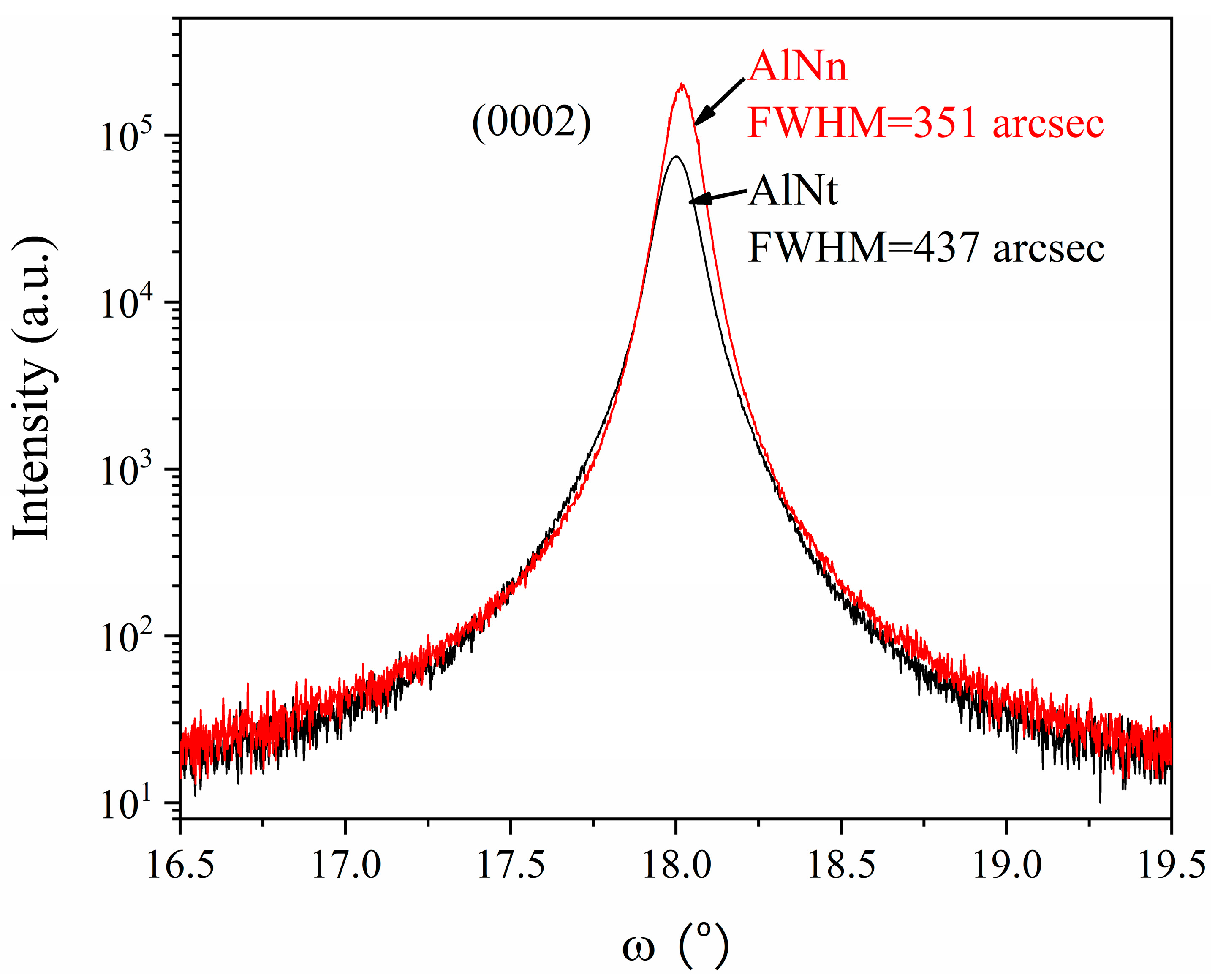
To analyze the structural characteristics of two AlN samples and compare their crystal quality, the X-ray rocking curves (XRC) of two samples were tested. As shown in
Figure 2, the crystal orientation (0002), (0004), and (0006) rocking curves of samples are measured, and the FWHM values are shown in
Table 1, which were obtained by Gaussian fitting.
The average grain size of the AlNt and AlNn can be estimated by the Debye–Sheller formula [
16,
31]:
where
D is the grain size (diameter),
β is the half-peak width of (0002) XRC,
k is the Scherrer constant (
k = 0.9),
λ is the X-ray diffraction wavelength (
λ = 0.15406 nm), and
θ is the diffraction angle.
The following Formula (2) can be used to calculate the microscopic strain (
ε) [
16,
31]:
where
θ is the diffraction angle and
β is the full width at half-maximum (FWHM).
In addition, the screw dislocation density of AlN can be evaluated by the following equation [
16,
31]:
where
β is the FWHM and
b is the length of the Burgers vector, which is 0.3110 nm.
Through the above calculation, the crystallite size, micro-strain, and screw dislocation density values of two samples are obtained, as shown in
Table 1. After comparison, the FWHM of AlNn is smaller than that of AlNt. The XRD symmetric (0002) linewidth was measured to be around 351 arcsec for AlNn and 437 arcsec for AlNt, respectively, indicating that the crystalline perfection of AlNn is better. Both AlN samples indicate low threading dislocation density. The thicker AlNn exhibits lower dislocations than another one; it is further proven that thick AlN epitaxial film can serve as a strain relief layer while significantly bending the dislocation and reducing total dislocation density. The reason can be explained below. With the increase of AlN thickness, the dislocation induced by the lattice mismatch between AlN epilayers and sapphire will gradually decrease and may even be annihilated, thus improving the crystal quality.
3.2. Optical Transmission Spectroscopy Analysis for AlN
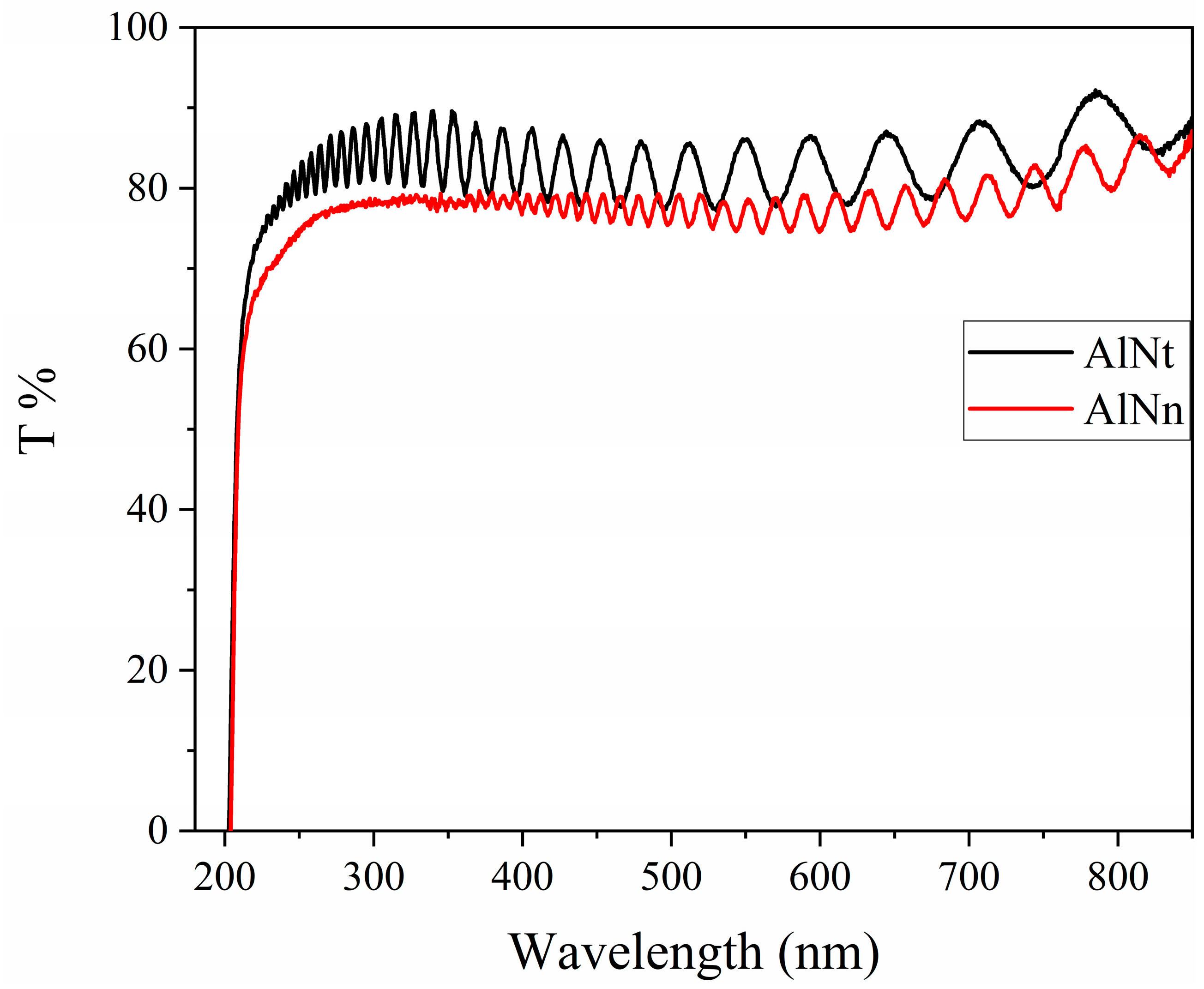
Figure 3 shows the optical transmission (OT) spectra of AlNt and AlNn samples, measured by a dual-beam ultraviolet-visible spectrophotometer. It can be observed that the absorption cut-off lines of both samples are very steep, indicating the advantage of thick film AlN. In the meantime, the spectra of the two samples show clear oscillations below the absorption edge, that is, the transparent region beyond 300 nm, indicating the advantages of this method of sample preparation, which can grow a film with a uniform distribution texture and excellent quality.
To better compare the two samples, AlNt and AlNn, the dependence of the absorption coefficient on photon energy can be used through the formula [
32]:
where
C is a constant,
is the bandgap of the semiconductor, and
is the photon energy.
The optical bandgap energy (
Eg) of AlN can be obtained by extrapolating the linear part of the proportional dependence of (
α)
2 vs. photon energy (
) by Formula (4), known as the Tauc plot [
32]. The values of
Eg can be calculated by linear fit close to the absorption edge (Dotted lines in green and purple), as shown in smaller image of
Figure 4. Where the smaller built-in image in
Figure 4 is the enlarged view of
Figure 4. Thus, the bandgap of the two samples can be seen in
Figure 4:
Eg (AlNt) = 6.08 ± 0.03 eV and
Eg (AlNn) = 6.05 ± 0.03 eV, as shown in
Table 2.
Figure 5 exhibits exponential absorption band tails below the band edge for both AlN samples, which may result from structural disorder accompanying electron–phonon coupling [
33,
34]. The Urbach’s binding energy (E
u), which is a band tail parameter, can be determined from the formula [
34]:
Figure 6 shows Urbach’s binding energy E
u compared with the FWHM of (0002) vs. the thickness of AlN. We obtain the E
u of AlNt and AlNn by OT as 117.56 meV and 99.97 meV, respectively. It shows that the obtained E
u (red solid squares in
Figure 6) is decreased with AlN epilayer thickness, which corresponds to the FWHM of HR-XRD results discussed before (black solid circles in
Figure 6), i.e., an improvement of structural quality. The high correlation between OT-derived E
u and HR-XRD FWHM predicates that the AlN crystalline quality can be demonstrated from the spectral properties in the vicinity of the band edge. The data for S1 (150 nm), S2 (300 nm), and S3 (400 nm) are from Ref. [
17] for comparison.
3.3. Cross-Sectional Morphologies of AlN
The thickness of the AlN film can also be determined by SEM on the AlN film cross-section. From
Figure 7, it can be obtained that the thicknesses of AlNt and AlNn samples are about 1.93 μm (AlNt) and 4.29 μm (AlNn), respectively. It can be seen that the AlN epitaxial layer in sample AlNn gradually becomes tightly packed, indicating that the crystal density of the AlN epitaxial layer is higher for a thick film, which corresponds to the XRD characterization.
3.4. Spectroscopic Ellipsometry Analysis of AlN
Spectroscopic ellipsometry (SE) measurements were performed for two AlN/sapphire samples, showing the changes in polarization states psi (Ψ) and delta (Δ) between the incidence and reflection of light on the sample. SE spectra of AlN samples are fitted using the J.A. Woollam Co. software to establish a four-phase physical model, including roughness/epitaxial AlN layer/AlN buffer layer/sapphire substrate. After fitting, the thickness, optical constants, surface roughness, and bandgap energy of the AlN epitaxial layer were derived. In the fitting model, a Bruggeman effective medium approximation was used to model the surface roughness. The optical constants of a sapphire substrate from Ref. [
35] were adopted and kept fixed in the fitting procedure. Two AlN layers are composed of a Gaussian oscillator, a PSemi-Tri oscillator, and a PSemi-MO oscillator. All parameters in AlN layers were adjusted to acquire the best-fitting SE data for two samples at room temperature (RT). The thicknesses of the AlN film, buffer layer, and surface roughness can be obtained within reasonable boundaries.
Figure 8a,b presents the experimental SE spectra and fitting curves of psi (Ψ) and delta (Δ) at 300 K with three incident angles of 60°, 65°, and 70° for two AlN samples. The experimental and fitting results are in good agreement. The interference oscillations below the bandgap edge correspond to the transparent region of the AlN sample. The final fitting results with parameters of the surface roughness, epilayer, and interlayer thicknesses for both AlN samples are listed in
Table 2. In the meantime, the optical constants of AlNt and AlNn samples, such as refractive index (n) and extinction coefficient (k), vs. the photon energy, are extracted by SE fitting at 300 K and shown in
Figure 9. The optical bandgap energy (
Eg) of AlN can be obtained by extrapolating the linear part of the proportional dependence of (
α)
2 vs. photon energy (
) by Formula (4), known as the Tauc plot [
32]. Thus, the bandgap of the two samples can be seen in
Figure 10:
Eg (AlNt) = 6.11 ± 0.01 eV and
Eg (AlNn) = 6.10 ± 0.02 eV, as shown in
Table 2.
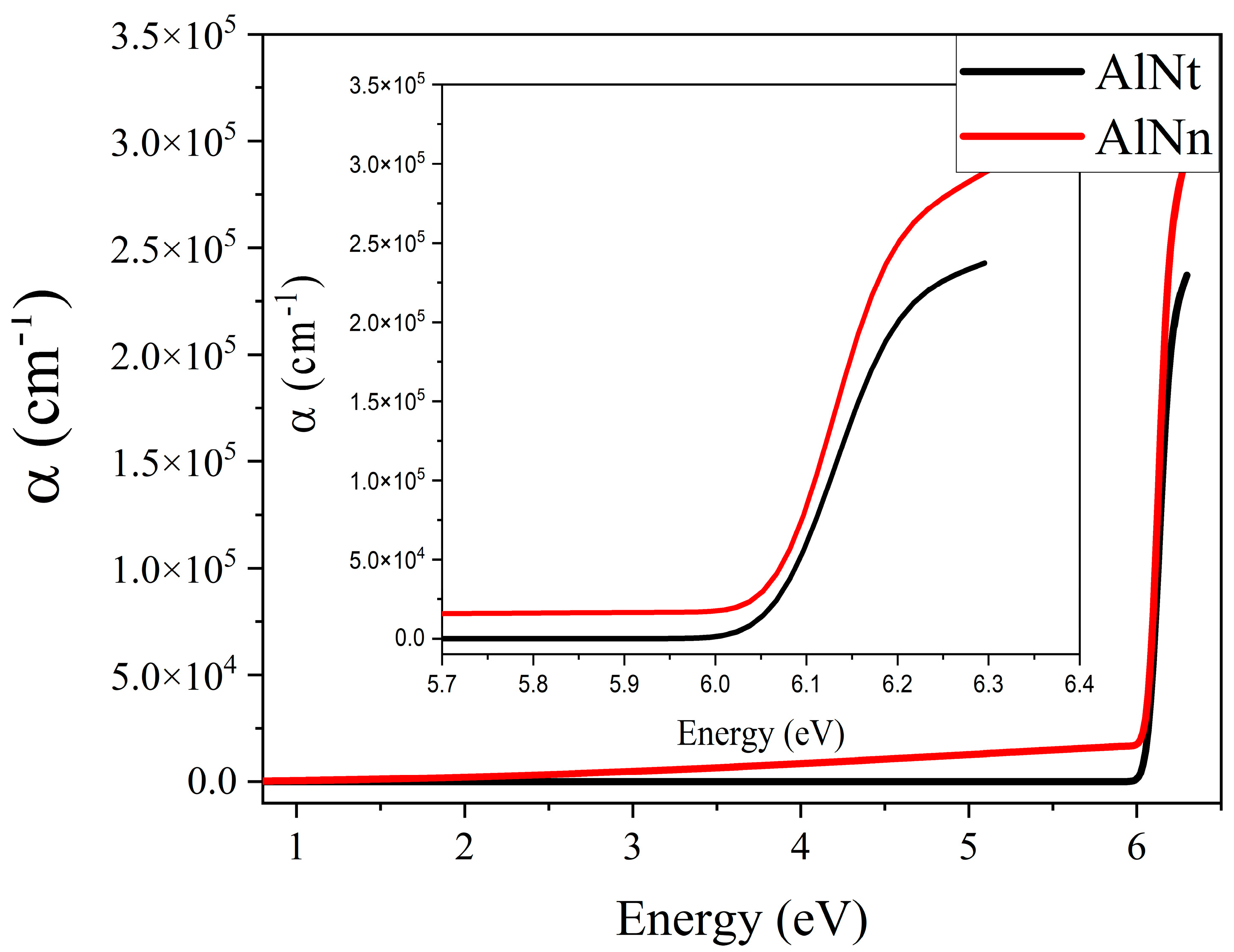
Figure 11 shows the absorption coefficient (
α) of epilayer vs. photon energy (
), according to
α = 4πk/
λ, where k is the extinction coefficient. From
Figure 11, below the band-edge, the absorption band tail is observed for two AlN samples, which could originate from the structural disorder accompanying electron–phonon coupling [
17]. The band tail parameters E
u of AlNt and AlNn can be obtained by Formula (5), which are 50.08 meV and 45.48 meV, respectively, as shown in
Figure 12 and
Table 2. Through comparison, it can be found that the changing trend of these two parameters from OT and SE is consistent with the results of XRD from
Figure 13, which proves the accuracy of SE characterization. Meanwhile, it is also observed that the result of E
u obtained by SE is much smaller than OT. The reason is that the data from the OT test is the combination of the entire AlN epitaxial layer and buffer layer, while the data taken from SE is directly from the epitaxial layer. The epitaxial layer usually has better quality and a lower density of defects than the interlayer, so the E
u value is smaller by SE than by OT. The bandgap of two samples can be acquired by Formula (4) as shown in
Figure 10:
Eg (AlNt) = 6.11 ± 0.01 eV and
Eg (AlNn) = 6.10 ± 0.02 eV, as indicated in
Table 2. The values of the bandgap obtained by SE are slightly larger than those measured by OT. The reason is that the bandgap obtained by the OT method is the bandgap including interlayer and epi-layer, while the bandgap obtained by the SE method is only the bandgap of epi-layer, and the bandgap is affected by the band edge, so the Urbach band tail characterized by SE is smaller, resulting in a larger bandgap characterized by SE. With the increase in epitaxial layer thickness, some of the dislocations will annihilate, and the quality of AlN films will tend to be better.
3.5. Temperature-Dependent SE Analysis of AlN
To understand the influence of temperature on the optical properties of AlN epi-films, a variable-temperature ellipsometry experiment was carried out. Based upon the accuracy of the SE dispersion model and fitting results, the room-temperature fitting parameters of the model were used as the initial values for subsequent high-temperature fitting. Then, the relevant parameters are adjusted, and the surface roughness, film, and interlayer thicknesses are further fitted to match the SE data of the high-temperature experiment. A special concern is the study of the changes in bandgap energy (
Eg), refractive index (n), and extinction coefficient (k) with temperature.
Figure 14a–h show the refractive index (n) and extinction coefficient (k) vs. photon energy at different temperatures, where
Figure 14b,d,f,h are enlarged views of
Figure 14a,c,e,g, respectively. It indicates that the n and k values shift from right to left as the temperature increases.
Figure 15a,b show (
)
2 vs. photon energy (
) of AlNt and AlNn at 12 temperature points between 300 K and 850 K. The optical bandgap energy (
Eg) of AlN can be obtained by extrapolating the linear part of the proportional dependence of (
α)
2 vs. photon energy (
) by Formula (4) [
32]. It is observed that with the temperature rising, the absorption edge shifts to the lower energy, together with the enlarged band tailing, i.e., the redshift of the bandgap.
Figure 16 depicts the dependence of the bandgap on temperature (
T) for the two AlN films. The bandgap energy of both samples exhibits an apparent redshift with the increase in temperature. These results are due to the dominant electron–phonon interactions being stronger than the weak contribution of thermal expansion [
36,
37].
The change of the bandgap with temperature can be fitted using Bose–Einstein’s analytical formula [
29],
where
θ is related to the average phonon temperature,
represents the strength of the average electron–phonon coupling. The fitting results are presented in
Figure 16 and
Table 3. It is seen that the fitting degree of accuracy is very high due to one of the values being extremely close to a value of 1 for Adj.R-Square. The solid lines in
Figure 16 show the trend of the bandgap with temperature.
Table 3 also lists the fitted values of
and
θ from Ref. [
17] for comparison. We can see that the reported data in Ref. [
17] are all larger than those obtained by our present work, indicating that the larger the thickness, the weaker the electron–phonon coupling and the following slower decline of
Eg. However, in this study, the
of the two samples was similar, and the declining value of
Eg was similar. This result may predict that when the thickness increases to a certain value (micrometer order), the thickness has little effect on the change of
Eg with temperature, which indicates the thermal stability of
Eg for thick AlN films. Combined with the changing trend of the Urbach band tail of five samples in
Figure 6, we can also find that the declining trend of the Urbach band tail E
u becomes smaller when the thickness of the sample reaches the micron level. The reason for these two kinds of similar phenomena may be that when the thickness reaches the micron level, all the islands in the growth of AlN coalesce together, and the dislocations induced by lattice mismatch diminish gradually, so the influence of thickness on thermal stability will become smaller.
4. Conclusions
In summary, the optical and structural characteristics of AlN films grown on sapphire substrates by MOCVD have been investigated by way of HRXRD, OT, SEM, and SE, especially focused on optical properties at high-temperatures by temperature-dependent SE. The thicker AlNn exhibits lower dislocations than the thinner ones; it is further proven that thick AlN epitaxial samples can serve as a strain relief layer, significantly bend the dislocation, and reduce total dislocation density. The reason is that, with the increase in AlN thickness, the dislocation arising from the lattice mismatch between AlN and sapphire will be gradually decreased and may even be annihilated, thus improving the sample’s crystalline quality. Urbach’s binding energy Eu and optical bandgap Eg by OT and SE depend on crystallite alignment, crystalline size, and film thickness, which are highly by XRD and SEM results. With the combination of SE, HRXRD, and OT analyses, we concluded that with the treatment of thickening film, the essence of crystal quality improved. However, the bandgap energies obtained from SE have larger values and higher accuracy than those extracted from OT. It has been proven that SE measurement is an efficient and useful method to characterize semiconductor thin films. The Bose–Einstein relation is used to demonstrate the temperature dependence of the bandgap. Our results reveal that the thermal stability of the AlN bandgap energy can be improved by increasing film thickness, which is caused by the corresponding weaker electron–phonon interactions. However, when the thickness increases to micrometer order, the thickness has little effect on the change of Eg with temperature. The AlN film with epilayer thicknesses of 1.776 and 3.666 µm has a small average electron–phonon coupling of about 390 meV. These results and analyses will provide good information for further penetrative research for AlN-based devices such as SAW sensors, LDs, LEDs, and other optoelectronic devices, especially those working at high temperatures.
Author Contributions
Conceptualization, Y.Y., L.W. (Lianshan Wang), W.S., Y.L. and Z.C.F.; methodology, Y.Y., Y.L. and Z.C.F.; software, Y.Y.; validation, S.Z., H.L., Y.P., W.W. and J.Y.; formal analysis, Y.Y.; investigation, Y.Y., S.Z., H.L., Y.P., W.W. and J.Y.; resources, L.W. (Lianshan Wang), L.W. (Lingyu Wan) and W.S.; data curation, Y.Y., Y.L. and Z.C.F.; writing—original draft preparation, Y.Y.; writing—review and editing, L.W. (Lianshan Wang), Y.L., Z.C.F., Y.Y., I.T.F., B.K. and W.S.; supervision, I.T.F., B.K., L.W. (Lingyu Wan), and Z.C.F., project administration, L.W. (LianshanWang), Y.L., Z.C.F. and W.S.; funding acquisition, L.W. (Lianshan Wang), Y.L. and W.S. All authors have read and agreed to the published version of the manuscript.
Funding
This work was partially supported by the National Key R&D Program of China (Grant Nos. 2022YFB3605100 and 2022YFB3605101), high luminous efficiency and long-life DUV LED technology (Grant No. AC22080003), Disinfection Robot Based on High Power AlGaN-based UVLEDs (Grant No. BB31200014), the Guangxi Science and Technology Program (Grant Nos. AD19245132 and A3120051010), the Guangxi Science and Technology Base and Talent Special Project (Grant No. AD20238093), and the Doctoral Research Start-up Foundation of Guangxi University (Grant No. XBZ2201513).
Institutional Review Board Statement
Not applicable.
Informed Consent Statement
Not applicable.
Data Availability Statement
The data presented in this study are available on request from the corresponding authors.
Conflicts of Interest
The authors declare no conflict of interest.
References
- Motamedi, P.; Cadien, K. Structural and optical characterization of low-temperature ALD crystalline AlN. J. Cryst. Growth 2015, 421, 45–52. [Google Scholar] [CrossRef]
- Taniyasu, Y.; Kasu, M.; Makimoto, T. An aluminum nitride light-emitting diode with a wavelength of 210 nanometers. Nature 2006, 441, 325–328. [Google Scholar] [CrossRef] [PubMed]
- Sun, X.; Li, D.; Chen, Y.; Song, H.; Jiang, H.; Jiang, Z.; Li, Z.; Miao, G.; Zhang, Z. In situ observation of two-step growth of AlN on sapphire using high-temperature metal-organic chemical vapor deposition. CrystEngComm 2013, 15, 6066–6073. [Google Scholar] [CrossRef]
- Liu, Z.Y.; Nong, M.T.; Lu, Y.; Cao, H.C.; Yuvaraja, S.; Xiao, N.; Alnakhli, Z.; Vázquez, R.R.A.; Li, X.H. Effect of the AlN strain compensation layer on InGaN quantum well red-light-emitting diodes beyond epitaxy. Opt. Lett. 2023, 47, 6229–6232. [Google Scholar] [CrossRef] [PubMed]
- Kim, N.; Yarali, M.; Moradnia, M.; Mehmood, M.A.; Liao, C.H.; AlQatari, F.; Nong, M.T.; Li, X.H.; Ryou, J.H. Piezoelectric Sensors Operating at Very High Temperatures and in Extreme Environments Made of Flexible Ultrawide-Bandgap Single-Crystalline AlN Thin Films. Adv. Funct. Mater. 2022, 33, 2212538. [Google Scholar] [CrossRef]
- Bersch, B.C.; Caminal Ros, T.; Tollefsen, V.; Johannessen, E.A.; Johannessen, A. Improved Crystallinity of Annealed 0002 AlN Films on Sapphire Substrate. Materials 2023, 16, 2319. [Google Scholar] [CrossRef] [PubMed]
- Kneissl, M.; Seong, T.; Han, J.; Amano, H. The emergence and prospects of deep-ultraviolet light-emitting diode technologies. Nat. Photonics 2019, 13, 233–244. [Google Scholar] [CrossRef]
- Jena, D.; Gossard, A.C.; Mishra, U.K. Dislocation scattering in a two-dimensional electron gas. Appl. Phys. Lett. 2000, 76, 1707–1709. [Google Scholar] [CrossRef]
- Mei, J.; Ponce, F.A.; Fareed, R.S.Q.; Yang, J.W.; Asif Khan, M. Dislocation generation at the coalescence of aluminum nitride lateral epitaxy on shallow-grooved sapphire substrates. Appl. Phys. Lett. 2007, 90, 221909. [Google Scholar] [CrossRef]
- Marino, F.A.; Faralli, N.; Palacios, T.; Ferry, D.K.; Goodnick, S.M.; Saraniti, M. Effects of threading dislocations on AlGaN/GaN high-electron mobility transistors. IEEE Trans. Electron Devices 2010, 57, 353–360. [Google Scholar] [CrossRef]
- Kaun, H.S.W.; Burke, P.G.; Hoi Wong, M.; Kyle, E.C.H.; Mishra, U.K.; Speck, J.S. Effect of dislocations on electron mobility in AlGaN/GaN and AlGaN/AlN/GaN heterostructures. Appl. Phys. Lett. 2012, 101, 262102. [Google Scholar] [CrossRef]
- Coltrin, M.E.; Creighton, J.R.; Mitchell, C.C. Modeling the parasitic chemical reactions of AlGaN organometallic vapor-phase epitaxy. J. Cryst. Growth 2006, 287, 566–571. [Google Scholar] [CrossRef]
- Imura, M.; Nakano, K.; Fujimoto, N.; Okada, N.; Balakrishnan, K.; Iwaya, M.; Kamiyama, S.; Amano, H.; Akasaki, I.; Noro, T. High-temperature metal-organic vapor phase epitaxial growth of AlN on sapphire by multi transition growth mode method varying V/III ratio. Jpn. J. Appl. Phys. 2006, 45, 8639–8643. [Google Scholar] [CrossRef]
- Imura, M.; Nakano, K.; Fujimoto, N.; Okada, N.; Balakrishnan, K.; Iwaya, M.; Kamiyama, S.; Amano, H.; Akasaki, I.; Noro, T. Dislocations in AlN epilayers grown on sapphire substrate by high-temperature metal-organic vapor phase epitaxy. Jpn. J. Appl. Phys. 2007, 46, 1458–1462. [Google Scholar] [CrossRef]
- Feng, Z.C.; Yang, H.; Yin, J.H.; Liu, Y.; Wu, F.; Dai, J.N.; Chen, C.Q.; He, K.Y.; Wan, L.Y.; Saravade, V.; et al. Crystalline and optical properties of AlN films with varying thicknesses (0.4-10 µm) grown on sapphire by metalorganic chemical vapor deposition. Thin Solid Films 2023, 780, 139939. [Google Scholar] [CrossRef]
- Yin, J.H.; Chen, D.H.; Yang, H.; Liu, Y.; Talwar, D.N.; He, T.L.; Ferguson, I.T.; He, K.Y.; Wan, L.Y.; Feng, Z.C. Comparative spectroscopic studies of MOCVD grown AlN films on Al2O3 and 6H-SiC. J. Alloy. Compd. 2021, 857, 157487. [Google Scholar] [CrossRef]
- Liu, Y.; Yang, Z.; Long, X.; Zhang, X.; Feng, Z.C. Effects of thickness and interlayer on optical properties of AlN films at room and high temperature. J. Vac. Sci. Technol. A 2021, 39, 043402. [Google Scholar] [CrossRef]
- Wei, W.W.; Peng, Y.; Wang, J.B.; Saleem, M.F.; Wang, W.; Li, L.; Wang, Y.K.; Sun, W.H. Temperature Dependence of Stress and Optical Properties in AlN Films Grown by MOCVD. Nanomaterials 2021, 11, 698. [Google Scholar] [CrossRef]
- Zhang, S.P.; Yang, H.; Wang, L.S.; Cheng, H.; Lu, H.X.; Yang, Y.L.; Wan, L.Y.; Xu, G.; Feng, Z.C.; Klein, B.; et al. Structural, Surface and Optical Studies of m- and c-Face AlN Crystals Grown by Physical Vapor Transport Method. Materials 2023, 16, 1925. [Google Scholar] [CrossRef]
- Nath, D.; Chakravarty, S.; Gupta, M.; Deshpande, U.P.; Abinash Bhuyan, C.; Chandra Shekar, N.V. Investigation of dilute ferromagnetism induced at room temperature in undoped crystalline AlN thin film after isothermal annealing in a controlled oxygen environment. J. Alloy. Compd. 2023, 967, 171727. [Google Scholar] [CrossRef]
- Chen, S.; Zhang, X.; Wang, S.C.; Fan, A.J.; He, J.Q.; Li, C.; Lu, L.; Rao, L.F.; Zhuang, Z.; Hu, G.H.; et al. High quality non-polar a-plane AlN template grown on semi-polar r-plane sapphire substrate by three-step pulsed flow growth method. J. Alloy. Compd. 2021, 872, 159706. [Google Scholar] [CrossRef]
- Wu, H.D.; Ning, J.; Zhang, J.C.; Zeng, Y.; Jia, Y.Q.; Zhao, J.L.; Bai, L.; Wang, Y.B.; Li, S.Y.; Wang, D.; et al. High quality AlN film assisted by graphene/sputtered AlN buffer layer for deep-ultraviolet-LED. Nanotechnology 2003, 34, 295202. [Google Scholar] [CrossRef]
- Namikawa, G.; Shojiki, K.; Yoshida, R.; Kusuda, R.; Uesugi, K.; Miyake, H.; Miyake, H. MOVPE growth of AlN and AlGaN films on N-polar annealed and sputtered AlN templates. J. Cryst. Growth 2023, 617, 127256. [Google Scholar] [CrossRef]
- Zhu, Y.M.; Zheng, W.; Zhu, S.Q.; Ding, Y.; Jia, L.M.; Huang, F. Laser tuning in AlN single crystals. Sci. China Mater. 2021, 64, 2877–2882. [Google Scholar] [CrossRef]
- Chen, L.; Lin, W.; Chen, H.Y.; Xu, H.Q.; Guo, C.Y.; Liu, Z.B.; Yan, J.C.; Sun, J.; Liu, H.; Wu, J.; et al. Annihilation and Regeneration of Defects in (112) Semipolar AlN via High-Temperature Annealing and MOVPE Regrowth. Cryst. Growth Des. 2021, 21, 2911−2919. [Google Scholar] [CrossRef]
- Luo, X.G.; Zhang, X.; Chen, B.; Shen, Y.; Tian, Y.; Fan, A.J.; Chen, S.; Qian, Y.D.; Zhuang, Z.; Hu, G.H. Improved surface morphology and crystalline quality of semi-polar (112) AlN epilayer with dual moderate-temperature-grown AlN interlayers. Mat. Sci. Semicon. Proc. 2022, 144, 106612. [Google Scholar] [CrossRef]
- Wang, J.M.; Xie, N.; Xu, F.J.; Zhang, L.S.; Lang, J.; Kang, X.N.; Qin, Z.X.; Yang, X.L.; Tang, N.; Wang, X.Q.; et al. Group-III nitride heteroepitaxial films approaching bulk-class quality. Nat. Mater. 2023, 22, 853–859. [Google Scholar] [CrossRef]
- Hasan, S.; Mamun, A.; Hussain, K.; Patel, D.; Gaevski, M.; Ahmad, I.; Khann, A. Investigation of MOCVD grown crack-free 4 μm thick aluminum nitride using nitrogen as a carrier gas. MRS Adv. 2021, 6, 456–460. [Google Scholar] [CrossRef]
- Nam, K.; Li, J.; Lin, J.; Jiang, H. Optical properties of AlN and GaN in elevated temperatures. Appl. Phys. Lett. 2004, 85, 3489–3491. [Google Scholar] [CrossRef]
- He, H.; Huang, L.; Zhang, Y.; Fu, Y.; Shen, X.; Zeng, J. Temperature dependence of the bandgap and Urbach’s tail in the transmittance spectra of wurtzite AlN film. Vacuum 2014, 100, 33–35. [Google Scholar] [CrossRef]
- Khedmi, N.; Ben Rabeh, M.; Kanzari, M. Structural morphological and optical properties of SnSb2S4 thin films grown by vacuum evaporation method. J. Mater. Sci. Technol. 2014, 30, 1006–1011. [Google Scholar] [CrossRef]
- Ahmad, A.A.; Alsaad, A.M.; Albiss, B.A.; Al-Akhras, M.A.; El-Nasser, H.M.; Qattan, I.A. Optical and structural properties of sputter deposited ZnO thin films in relevance to post-annealing and substrate temperatures. Thin Solid Films 2016, 606, 133–142. [Google Scholar] [CrossRef]
- Jiang, L.F.; Shen, W.Z.; Ogawa, H.; Guo, Q.X. Temperature dependence of the optical properties in hexagonal AlN. J. Appl. Phys. 2003, 94, 5704–5709. [Google Scholar] [CrossRef]
- Ahmad, A.A.; Alsaad, A.M.; Albiss, B.A.; Al-Akhras, M.A.; El-Nasser, H.M.; Qattan, I.A. The effect of substrate temperature on structural and optical properties of D.C. sputtered ZnO thin films. Physica B 2015, 21, 470–471. [Google Scholar] [CrossRef]
- Palik, E.D. Handbook of Optical Constants of Solids; Elsevier: London, UK, 1997. [Google Scholar]
- Sohal, S.; Feng, W.; Pandikunta, M.; Kuryatkov, V.V.; Nikishin, S.A.; Holtz, M. Influence of phonons on the temperature dependence of the band gap of AlN and AlxGa1-xN alloys with high AlN mole fraction. J. Appl. Phys. 2013, 113, 043501. [Google Scholar] [CrossRef]
- Tisch, U.; Meyler, B.; Katz, O.; Finkman, E.; Salzman, J. Dependence of the refractive index of AlxGa1-xN on temperature and composition at elevated temperatures. J. Appl. Phys. 2001, 89, 2676–2685. [Google Scholar] [CrossRef]
Figure 1.
XRD-wide scans of AlNt and AlNn, showing AlN (0002), (0004), and (0006).
Figure 1.
XRD-wide scans of AlNt and AlNn, showing AlN (0002), (0004), and (0006).
Figure 2.
(0002) XRC of AlNt and AlNn by HR-XRD.
Figure 2.
(0002) XRC of AlNt and AlNn by HR-XRD.
Figure 3.
Optical transmission spectra of AlNt and AlNn.
Figure 3.
Optical transmission spectra of AlNt and AlNn.
Figure 4.
Calculated ()2 vs. photon energy () for two AlN epi-films by OT.
Figure 4.
Calculated ()2 vs. photon energy () for two AlN epi-films by OT.
Figure 5.
The relation between ln and photon energy () by OT.
Figure 5.
The relation between ln and photon energy () by OT.
Figure 6.
Comparison between FWHM (0002) by HR-XRD and Urbach’s binding energy (E
u) as a function of AlN epi-film thickness by OT. The data for S1 (150 nm), S2 (300 nm), and S3 (400 nm) are from Ref. [
17] for comparison.
Figure 6.
Comparison between FWHM (0002) by HR-XRD and Urbach’s binding energy (E
u) as a function of AlN epi-film thickness by OT. The data for S1 (150 nm), S2 (300 nm), and S3 (400 nm) are from Ref. [
17] for comparison.
Figure 7.
Cross-sectional SEM micrographs of AlNt and AlNn.
Figure 7.
Cross-sectional SEM micrographs of AlNt and AlNn.
Figure 8.
(a) Polarization states Ψ (λ) and Δ (λ) spectra of AlNt at room temperature, where the color dotted line and black solid line represent experimental measured data and model fitted data, respectively. (b) Polarization states Ψ (λ) and Δ (λ) spectra of AlNn at room temperature, where the color dotted line and black solid line represent experimental measured data and model fitted data, respectively.
Figure 9.
Fitted optical constants (refractive index n and extinction coefficient k) of two AlN samples at room temperature by SE.
Figure 9.
Fitted optical constants (refractive index n and extinction coefficient k) of two AlN samples at room temperature by SE.
Figure 10.
Calculated ()2 vs. photon energy () for two AlN epi-films by SE.
Figure 10.
Calculated ()2 vs. photon energy () for two AlN epi-films by SE.
Figure 11.
The absorption coefficient of two AlN samples at room temperature by SE.
Figure 11.
The absorption coefficient of two AlN samples at room temperature by SE.
Figure 12.
The relation between ln () and photon energy () by SE.
Figure 12.
The relation between ln () and photon energy () by SE.
Figure 13.
Comparison between FWHM (0002) by HR-XRD and Urbach’s binding energy (Eu) as a function of AlN epi-film thickness by SE.
Figure 13.
Comparison between FWHM (0002) by HR-XRD and Urbach’s binding energy (Eu) as a function of AlN epi-film thickness by SE.
Figure 14.
(a–h) n and k of AlNt and AlNn by VT-SE, where (b,d,f,h) are enlarged views of (a,c,e,g), respectively.
Figure 14.
(a–h) n and k of AlNt and AlNn by VT-SE, where (b,d,f,h) are enlarged views of (a,c,e,g), respectively.
Figure 15.
Relationship of ()2 vs. photon energy () for AlNt (a) and AlNn (b) epi-films by SE at a temperature range of 300–850 K.
Figure 15.
Relationship of ()2 vs. photon energy () for AlNt (a) and AlNn (b) epi-films by SE at a temperature range of 300–850 K.
Figure 16.
Temperature dependence of the bandgap energies from 300 K to 850 K for two AlN samples.
Figure 16.
Temperature dependence of the bandgap energies from 300 K to 850 K for two AlN samples.
Table 1.
(0002), (0004), and (0006) ω FWHM, calculation results of crystallite size, micro-strain, and dislocation density of two AlN epi-films.
Table 1.
(0002), (0004), and (0006) ω FWHM, calculation results of crystallite size, micro-strain, and dislocation density of two AlN epi-films.
| | | AlNt | AlNn |
|---|
| FWHM(0002)ω | (arcsec) | 438 ± 4 | 351 ± 5 |
| FWHM(0004)ω | (arcsec) | 434 ± 5 | 355 ± 6 |
| FWHM(0006)ω | (arcsec) | 531 ± 8 | 456 ± 8 |
| Crystallite size | (nm) | 68.72 ± 0.02 | 85.62 ± 0.03 |
| Micro-strain | (×10−3) | 0.50 ± 0.04 | 0.41 ± 0.05 |
| Screw dislocation density | (×10−5) (nm−2) | 1.07 ± 0.05 | 0.69 ± 0.06 |
Table 2.
A list of SE fitting results and OT results of AlN samples.
Table 2.
A list of SE fitting results and OT results of AlN samples.
| Sample Name | AlNt | AlNn |
|---|
| Surface roughness by SE (nm) | 3.07 ± 0.03 | 3.58 ± 0.05 |
| Thickness of epilayer by SE (nm) | 1776.35 ± 0.04 | 3666.17 ± 0.05 |
| Thickness of the buffer layer by SE (nm) | 21.27 ± 0.06 | 51.89 ± 0.06 |
| Thickness of AlN by SEM (μm) | 1.93 ± 0.05 | 4.29 ± 0.05 |
| Bandgap by SE (eV) | 6.11 ± 0.01 | 6.10 ± 0.02 |
| Bandgap by OT (eV) | 6.08 ± 0.03 | 6.05 ± 0.03 |
| Eu by SE (meV) | 50.08 ± 0.02 | 45.48 ± 0.02 |
| Eu by OT (meV) | 117.56 ± 0.03 | 99.97 ± 0.04 |
Table 3.
A list of fitting parameters for and from AlN samples.
Table 3.
A list of fitting parameters for and from AlN samples.
| Sample Name | Thickness | | | Adj.R-Square | Reference |
|---|
| (nm) | (meV) | (K) |
|---|
| AlNt | 1776.35 | 389 ± 100 | 800 ± 154 | 0.99645 | This work |
| AlNn | 3666.17 | 390 ± 102 | 795 ± 155 | 0.99639 | This work |
| S1 | 136.42 | 687 ± 72 | 1233 ± 73 | | Ref. [17] |
| S2 | 307.85 | 554 ± 54 | 1111 ± 64 | | Ref. [17] |
| S3 | 412.90 | 407 ± 36 | 977 ± 58 | | Ref. [17] |
| Disclaimer/Publisher’s Note: The statements, opinions and data contained in all publications are solely those of the individual author(s) and contributor(s) and not of MDPI and/or the editor(s). MDPI and/or the editor(s) disclaim responsibility for any injury to people or property resulting from any ideas, methods, instructions or products referred to in the content. |
© 2023 by the authors. Licensee MDPI, Basel, Switzerland. This article is an open access article distributed under the terms and conditions of the Creative Commons Attribution (CC BY) license (https://creativecommons.org/licenses/by/4.0/).

 ,
, 


