
Structural and Optical Characterizations of Cadmium Chalcogenide Layers on Polyamide Formed Using Monotelluropentathionic Acid


Abstract
:
1. Introduction
2. Materials and Methods
2.1. Materials
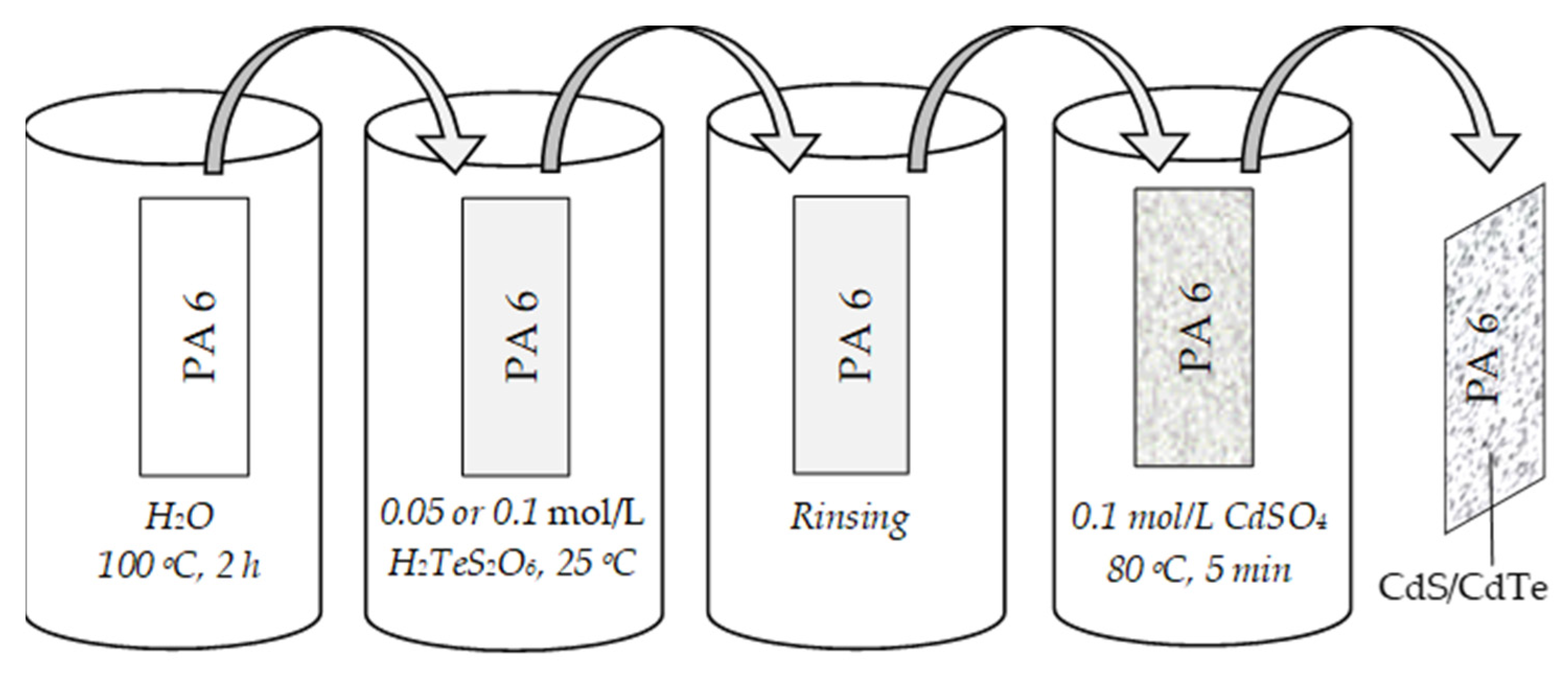
2.2. Cadmium Chalcogenides Layer Formation Materials
2.3. Instrumental Analysis
2.4. Modeling the Kinetics of Sorption
2.5. Optical Property Measurements
3. Results and Discussions
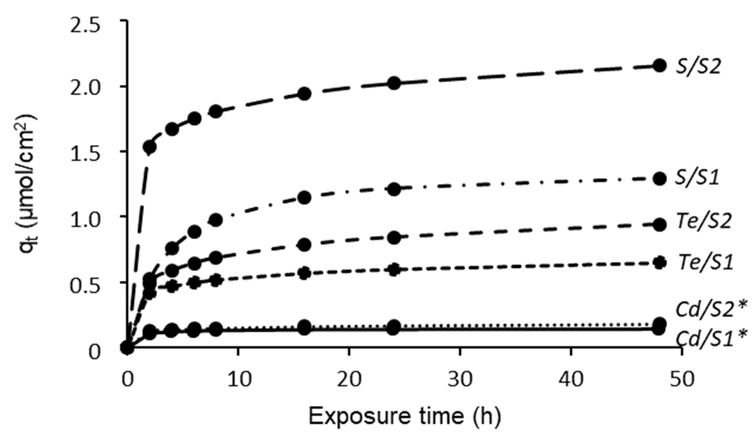
3.1. Chalcogens’ and Cadmium Adsorbtions Kinetics
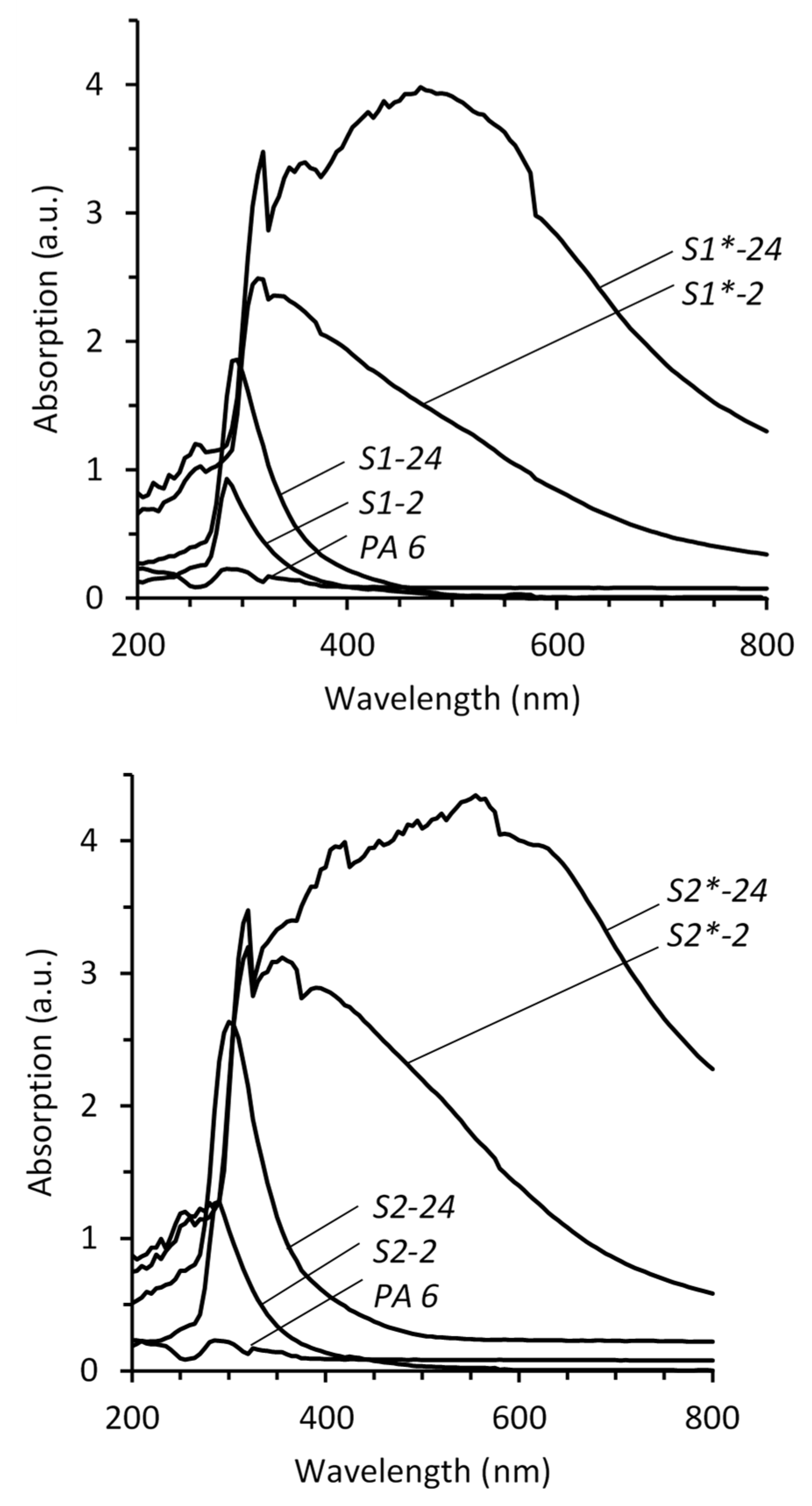
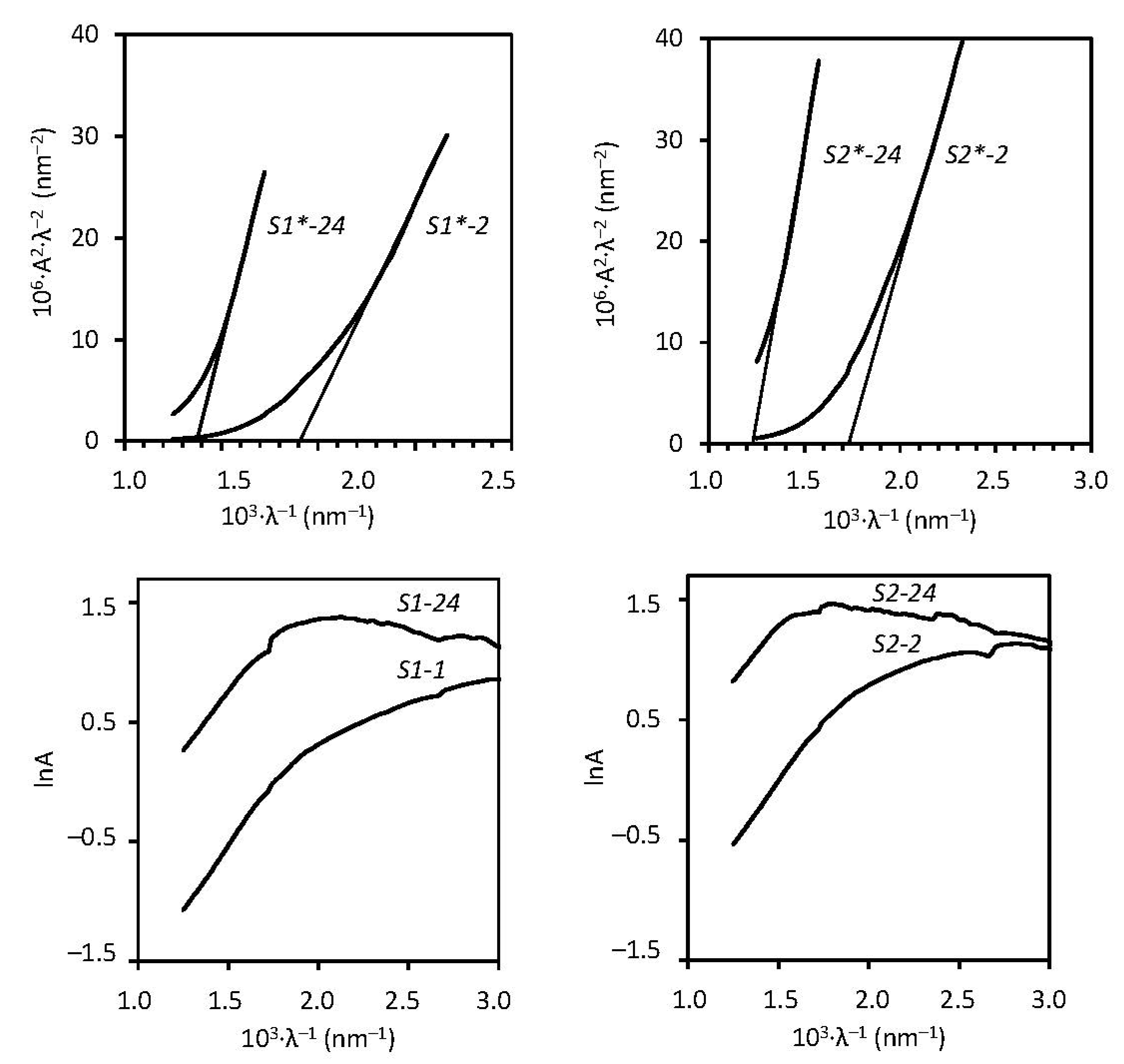
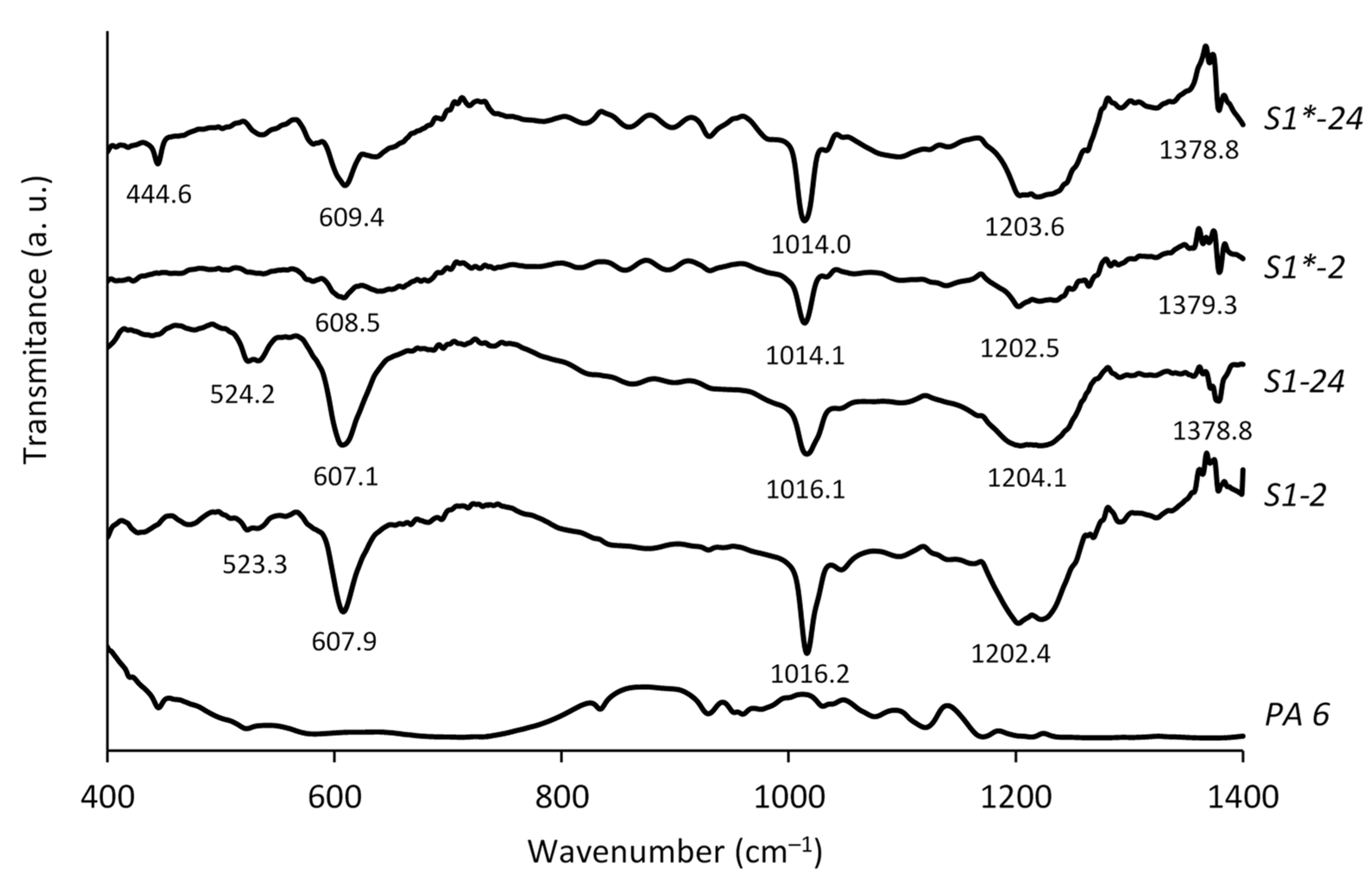
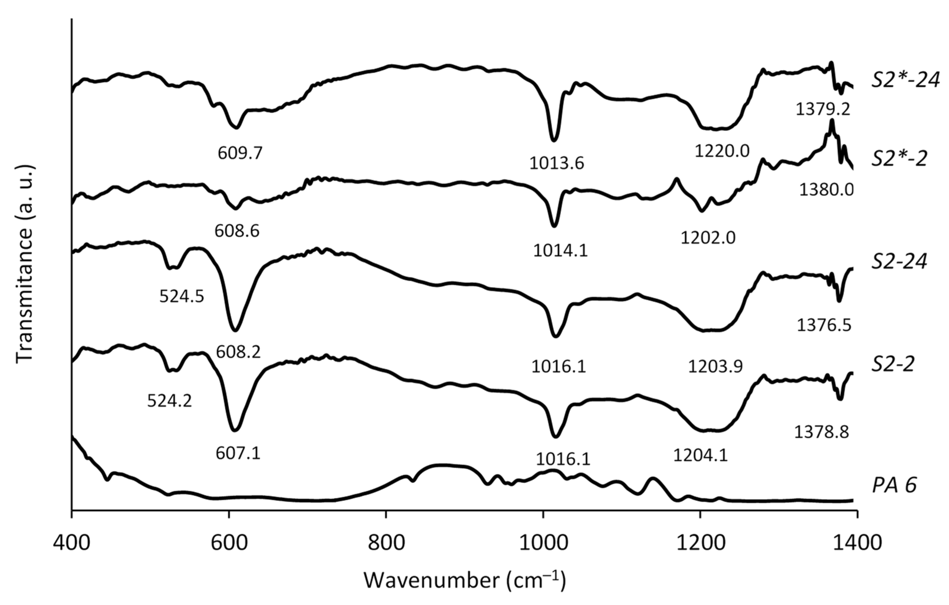
3.2. UV-Vis and FTIR Spectroscopies
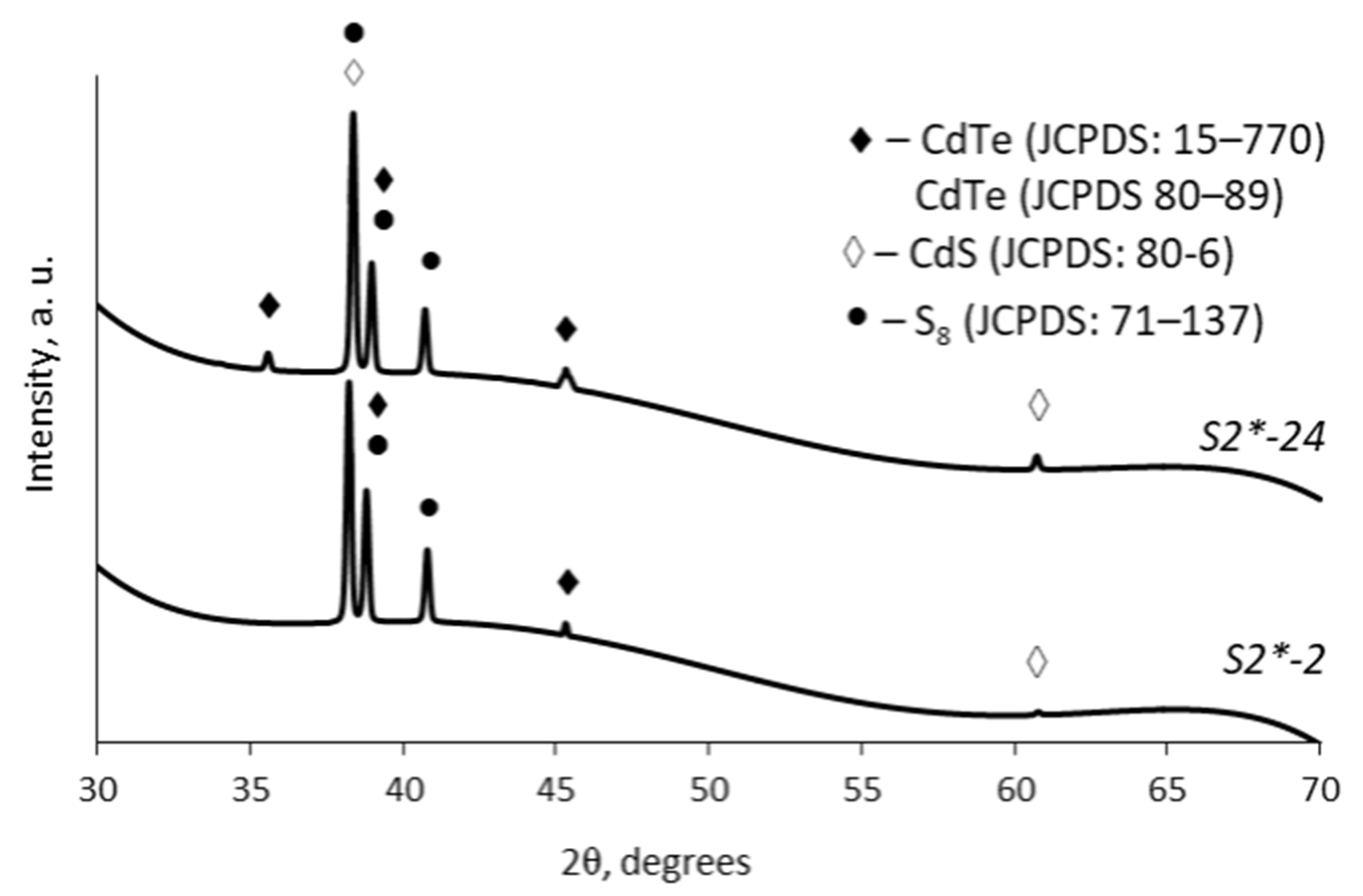
3.3. XRD Characterization and the Mechanism of Cadmium Chalcogenides Layers Formation on the Substrate of Polyamide 6 Film
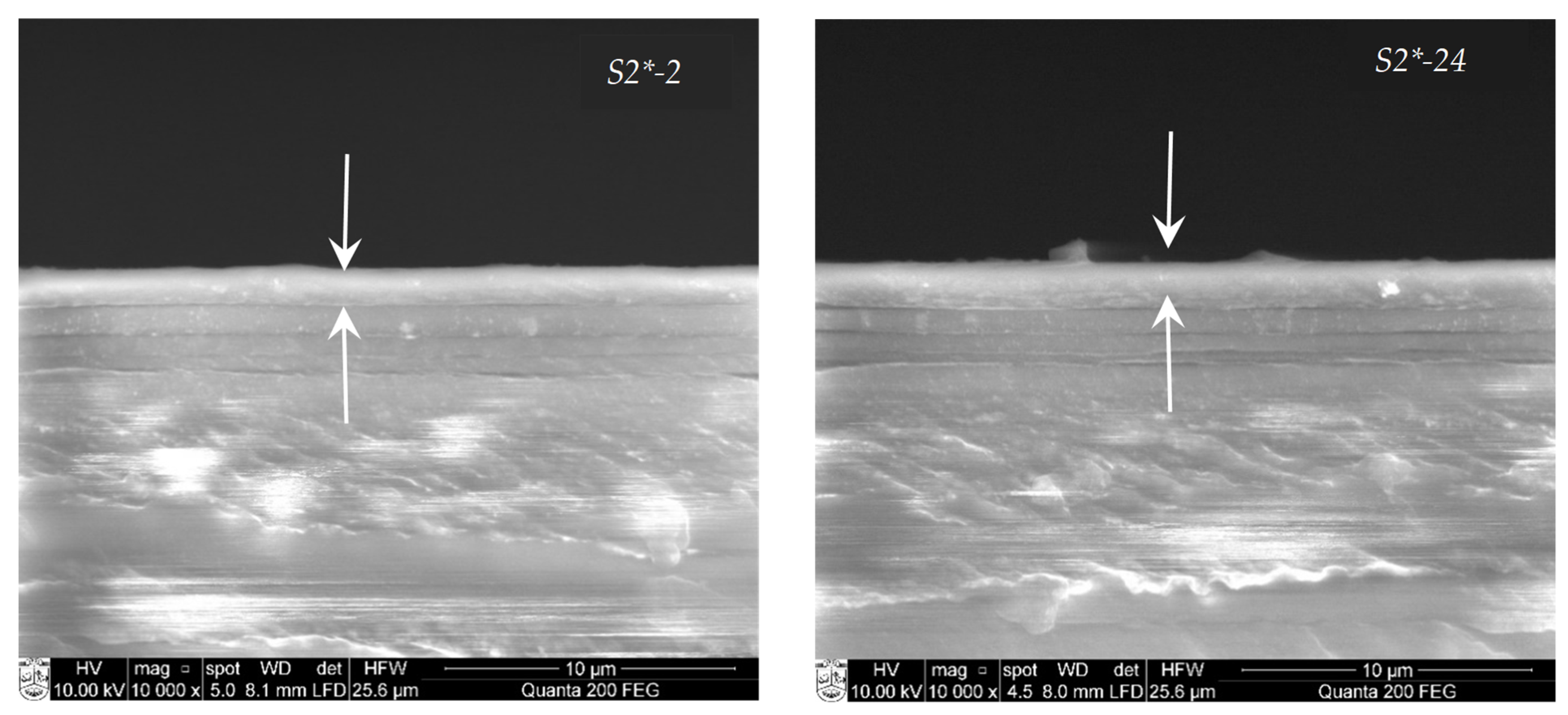
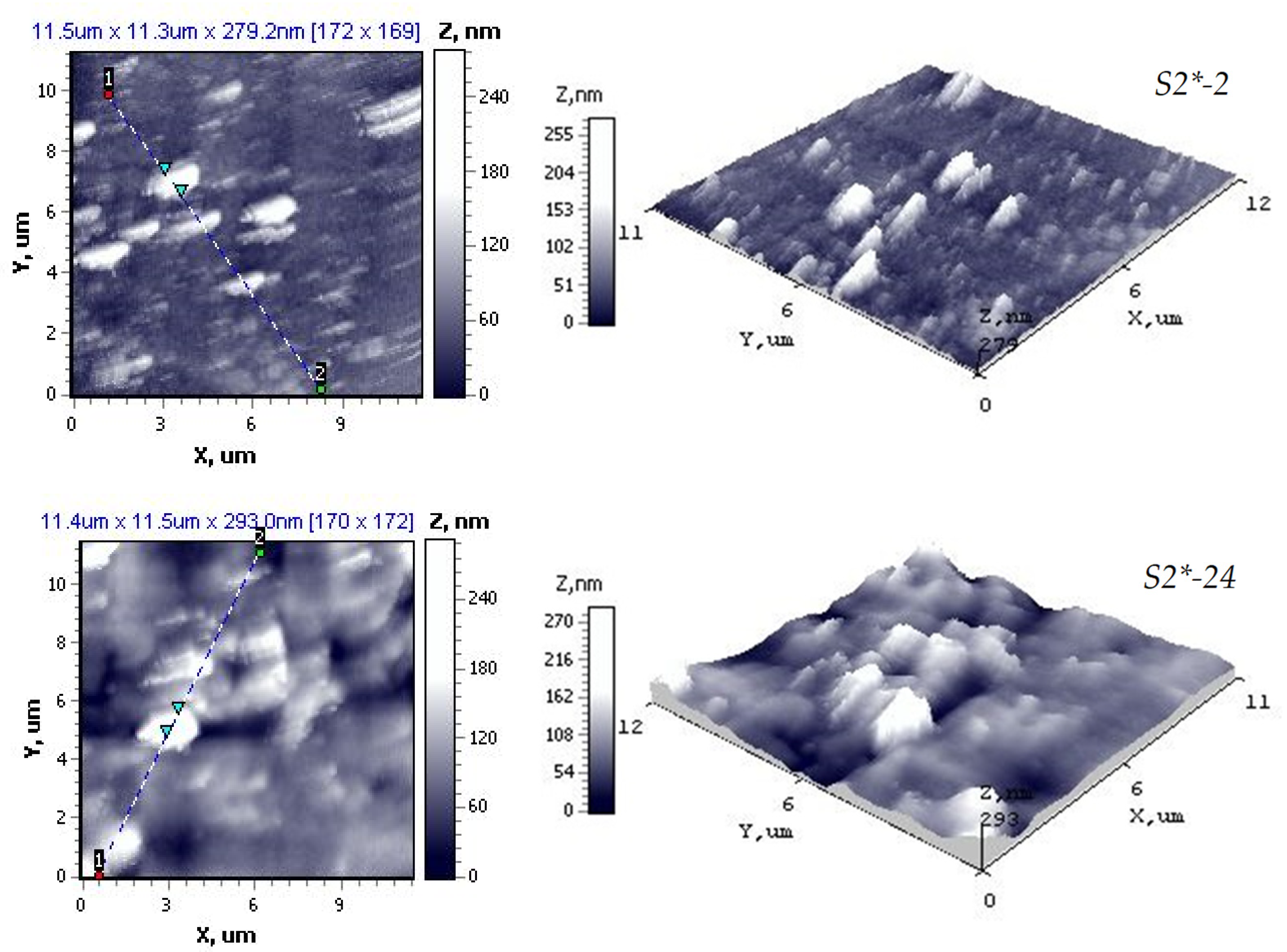
3.4. Morphological Characterization of Cadmium Chalcogenide Layers
4. Conclusions
Author Contributions
Funding
Institutional Review Board Statement
Informed Consent Statement
Data Availability Statement
Conflicts of Interest
References
- Zhang, X.; Wu, D.; Geng, H. Heterojunctions based on II-VI compound semiconductor one-dimensional nanostructures and their optoelectronic applications. Crystals 2017, 7, 307. [Google Scholar] [CrossRef] [Green Version]
- Ríos-González, J.A.; Mis-Fernández, R.; Camacho-Espinosa, E.; Riech, I.; Menéndez-Proupin, E.; Flores, M.A.; Orellana, W.; Peña, J.L. Inducing a level inside of CdTe bandgap doping with Sn using a co-sublimation technique by CSS. Mater. Sci. Semicond. Process. 2020, 107, 104836. [Google Scholar] [CrossRef]
- Halal, A.; Rahman, K.S.; Abdullah, S.F.; Sopian, K.; Amin, N. An investigation on CdS1-xTex interface compound in CdS/CdTe hetero-junction solar cells by density functional theory (DFT). Superlattices Microstruct. 2021, 151, 106805. [Google Scholar] [CrossRef]
- Supekar, A.; Kapadnis, R.; Bansode, S.; Bhujbal, P.; Kale, S.; Jadkar, S.; Pathan, H. Cadmium telluride/cadmium sulfide thin films solar cells: A review. ES Energy Environ. 2020, 10, 3–12. [Google Scholar] [CrossRef]
- Moreno-Regino, V.D.; Castañeda-de-la-Hoya, F.M.; Torres-Castanedo, C.G.; Márquez-Marín, J.; Castanedo-Pérez, R.; Torres-Delgado, G.; Zelaya-Ángel, O. Structural, optical, electrical and morphological properties of CdS films deposited by CBD varying the complexing agent concentration. Results Phys. 2019, 13, 102238. [Google Scholar] [CrossRef]
- Bosio, A.; Pasini, S.; Romeo, N. The history of photovoltaics with emphasis on CdTe solar cells and modules. Coatings 2020, 10, 344. [Google Scholar] [CrossRef] [Green Version]
- Nagaura, T.; Phan, H.P.; Malgras, V.; Pham, T.A.; Lim, H.; Ashok, A.; Kim, J.; You, J.; Nguyen, N.T.; Na, J.; et al. Universal electrochemical synthesis of mesoporous chalcogenide semiconductors: Mesoporous CdSe and CdTe thin films for optoelectronic applications. Angew. Chem. Int. Ed. 2021, 60, 9660–9665. [Google Scholar] [CrossRef]
- Maghouli, M.; Eshghi, H. Studying the effect of deposition time on physical properties of CdTe thin films; Influence of CdTe electrical properties on CdS/CdTe heterojunction rectifying behavior. Optik 2020, 218, 165132. [Google Scholar] [CrossRef]
- Wang, D.; Yang, Y.; Guo, T.; Xiong, X.; Xie, Y.; Li, K.; Li, B.; Ghali, M. Effect of pulse bias voltages on performance of CdTe thin film solar cells prepared by pulsed laser deposition. Sol. Energy 2021, 213, 118–125. [Google Scholar] [CrossRef]
- Saha, S.; Johnson, M.; Altayaran, F.; Wang, Y.; Wang, D.; Zhang, Q. Electrodeposition fabrication of chalcogenide thin films for photovoltaic applications. Electrochem 2020, 1, 19. [Google Scholar] [CrossRef]
- Maistruk, E.V.; Koziarskyi, I.P.; Koziarskyi, D.P.; Andrushchak, G.O. Optical properties of thin films cadmium chalcogenide obtained by the RF magnetron sputtering. Thirteen. Int. Conf. Correl. Opt. 2018, 10612, 277–284. [Google Scholar] [CrossRef]
- Carlos, V.-A. Self-powered cadmium chalcogenide photodetectors by pressurized air blast spraying. Opt. Mater. Express 2021, 11, 1104–1118. [Google Scholar] [CrossRef]
- Moger, S.N. Colour tunable co-evaporated CdSxSe1-x (0 ≤ x ≤ 1) ternary chalcogenide thin films for photodetector applications. Mater. Sci. Semicond. Process. 2020, 120, 105288. [Google Scholar] [CrossRef]
- Carcione, R.; Limosani, F.; Antolini, F. Cadmium telluride nanocomposite films formation from thermal decomposition of cadmium carboxylate precursor and their photoluminescence shift from green to red. Crystals 2021, 11, 253. [Google Scholar] [CrossRef]
- Yavorskyi, R.; Nykyruy, L.; Wisz, G.; Potera, P.; Adamiak, S.; Górny, S. Structural and optical properties of cadmium telluride obtained by physical vapor deposition technique. Appl. Nanosci. 2018, 9, 715–724. [Google Scholar] [CrossRef]
- Punitha, K.; Sivakumar, R.; Sanjeeviraja, C.; Sathe, V.; Ganesan, V. Physical properties of electron beam evaporated CdTe and CdTe:Cu thin films. J. Appl. Phys. 2014, 116, 213502. [Google Scholar] [CrossRef]
- Ivanauskas, R.; Milasiene, D. Fabrication of polyamide-Ag2Se composite films with controllable properties by an adsorption–diffusion method. J. Phys. Chem. Solids 2020, 145, 109533. [Google Scholar] [CrossRef]
- Ivanauskas, R.; Samardokas, L.; Mikolajunas, M.; Virzonis, D.; Baltrusaitis, J. Polyamide-thallium selenide composite materials via temperature and pH controlled adsorption-diffusion method. Appl. Surf. Sci. 2014, 317, 818–827. [Google Scholar] [CrossRef]
- Ancutiene, I.; Janickis, V.; Ivanauskas, R. Formation and characterization of conductive thin layers of copper sulfide (CuxS) on the surface of polyethylene and polyamide by the use of higher polythionic acids. Appl. Surf. Sci. 2006, 252, 4218–4225. [Google Scholar] [CrossRef]
- Šukytė, J.; Ivanauskas, R. Formation and properties of copper chalcogenides thin films on polymers formed using sodium telluropentathionate. Cent. Eur. J. Chem. 2013, 11, 1163–1171. [Google Scholar] [CrossRef] [Green Version]
- Ivanauskas, R.; Baltrusaitis, J. Synthesis and surface properties of polyamide-CuxSe composite thin films. Appl. Surf. Sci. 2013, 283, 360–366. [Google Scholar] [CrossRef]
- Phasook, N.; Kamoldirok, S.; Yindeesuk, W. Optical properties of Mn-doped CdS thin films grown by the SILAR method. J. Phys. Conf. Ser. 2018, 1144, 012009. [Google Scholar] [CrossRef]
- Chaudhari, K.B.; Gosavi, N.M.; Deshpande, N.G.; Gosavi, S.R. Chemical synthesis and characterization of CdSe thin films deposited by SILAR technique for optoelectronic applications. J. Sci. Adv. Mater. Devices 2016, 1, 476–481. [Google Scholar] [CrossRef]
- Hamid, Z.A.; Hassan, H.B.; Hassan, M.A.; Mourad, M.H.; Anwar, S. Deposition, characterization, performance of cadmium sulfide quantum dots thin films using SILAR technique for quantum dot sensitized solar cell applications. Key Eng. Mater. 2020, 835, 374–383. [Google Scholar] [CrossRef]
- Šukyte, V.J.; Ivanauskas, R.; Janickis, V. Preparation and some properties of Cu-Te-S thin films on the polyamide (PA) surface. Pol. J. Chem. 2005, 79, 759–771. [Google Scholar]
- Zalenkiene, S.; Sukyte, J.; Ivanauskas, R.; Janickis, V. Selenopentathionic and telluropentathionic acids as precursors for formation of semiconducting layers on the surface of polyamide. Int. J. Photoenergy 2007, 2007, 2660–2666. [Google Scholar] [CrossRef] [Green Version]
- Gregg, S.J.; Sing, K.S.W. Adsorption, Surface Area, and Porosity; Academic Press: London, UK, 1982; ISBN 0123009561. [Google Scholar]
- Olav Foss Salts of Monotelluropentathionic Acid. Available online: http://actachemscand.org/pdf/acta_vol_03_p0708-0716.pdf (accessed on 18 June 2021).
- Jeffery, G.H.; Passett, J.; Mendham, J.; Denney, R.C. Vogel’s Textbook of Quantitative Chemical Analysis. Available online: https://gtu.ge/Agro-Lib/Vogels_TEXTBOOK_OF_QUANTITATIVE_CHEMICAL_ANALYSIS_5th_ed__-_G_H_Jeffery.MsuCity.pdf (accessed on 18 June 2021).
- Ho, Y.S. Citation review of Lagergren kinetic rate equation on adsorption reactions. Scientometrics 2004, 59, 171–177. [Google Scholar]
- Ho, Y.S.; McKay, G. Pseudo-second order model for sorption processes. Process. Biochem. 1999, 34, 451–465. [Google Scholar] [CrossRef]
- Purwanto, P.; Riska, R. Kinetics and equilibrium studies of electro adsorption of remazol red on modified stainless steel electrode. J. Phys. Conf. Ser. 2019, 1295, 012045. [Google Scholar] [CrossRef] [Green Version]
- Wu, F.C.; Tseng, R.L.; Juang, R.S. Characteristics of Elovich equation used for the analysis of adsorption kinetics in dye-chitosan systems. Chem. Eng. J. 2009, 150, 366–373. [Google Scholar] [CrossRef]
- Boyd, G.E.; Adamson, A.W.; Myers, L.S. The exchange adsorption of ions from aqueous solutions by organic zeolites. II. Kinetics. J. Am. Chem. Soc. 1947, 69, 2836–2848. [Google Scholar] [CrossRef]
- Alkan, M.; Demirbaş, Ö.; Doǧan, M. Adsorption kinetics and thermodynamics of an anionic dye onto sepiolite. Microporous Mesoporous Mater. 2007, 101, 388–396. [Google Scholar] [CrossRef]
- El Fawal, G.F.; Khalifa, R.E.; Rahman, S.A.; Eldin, M.S.M. Poly (Methacrylic acid) grafted regenerated cellulose ions exchangers membranes for Cu(II) ion adsorption: Kinetic, isotherm, and thermodynamic studies. Desalination Water Treat. 2020, 178, 182–192. [Google Scholar] [CrossRef]
- Hamdaoui, O.; Naffrechoux, E. Modeling of adsorption isotherms of phenol and chlorophenols onto granular activated carbon. Part I. Two-parameter models and equations allowing determination of thermodynamic parameters. J. Hazard. Mater. 2007, 147, 381–394. [Google Scholar] [CrossRef] [PubMed]
- Hassanien, A.S.; Akl, A.A. Effect of Se addition on optical and electrical properties of chalcogenide CdSSe thin films. Superlattices Microstruct. 2016, 89, 153–169. [Google Scholar] [CrossRef]
- Ghobadi, N. Band gap determination using absorption spectrum fitting procedure. Int. Nano Lett. 2013, 3, 1–4. [Google Scholar] [CrossRef] [Green Version]
- Strehlow, W.H.; Cook, E.L. Compilation of energy band gaps in elemental and binary compound semiconductors and insulators. J. Phys. Chem. Ref. Data 1973, 2, 163–200. [Google Scholar] [CrossRef] [Green Version]
- Foss, O. Structure of compounds containing chains of sulfur atoms. In Advances in Inorganic Chemistry and Radiochemistry; Emeleus, H.J., Sharpe, A.G., Eds.; Academic Press Inc.: New York, NY, USA, 1960; pp. 237–278. [Google Scholar]
- Nakamoto, K. Infrared and raman spectra of inorganic and coordination compounds. In Handbook of Vibrational Spectroscopy; John Wiley & Sons, Ltd.: Hoboken, NJ, USA, 2006. [Google Scholar]
- Zhang, W.; Wong, P.K.J.; Chua, R.; Wee, A.T.S. Growth and properties of magnetic two-dimensional transition-metal chalcogenides. In Spintronic 2D Materials: Fundamentals and Applications; Elsevier: Amsterdam, The Netherlands, 2019; pp. 227–251. ISBN 9780081021545. [Google Scholar]
- Jing, Y.; Liu, B.; Zhu, X.; Ouyang, F.; Sun, J.; Zhou, Y. Tunable electronic structure of two-dimensional transition metal chalcogenides for optoelectronic applications. Nanophotonics 2020, 9, 1675–1694. [Google Scholar] [CrossRef]
- Keane, P.M.; Frazen, H.F. Chalcogenides: Solid State Chemistry; King, R.B., Ed.; John Wiley, Sons: Chichester, UK; New York, NY, USA; Brisbane, Australia; Toronto, ON, Canada; Singapore, 1994; Volume 7. [Google Scholar]
- Nelmes, R.J.; McMahon, M.I.; Wright, N.G.; Allan, D.R. Observation of a high-pressure cinnabar phase in CdTe. Phys. Rev. B 1993, 48, 1314–1317. [Google Scholar] [CrossRef]
- Templeton, L.K.; Templeton, D.H.; Zalkin, A. Crystal structure of monoclinic sulfur. Inorg. Chem. 1976, 15, 1999–2001. [Google Scholar] [CrossRef] [Green Version]
- Swanson, H.E.; Morris, M.C.; Evans, E.; Ulmer, L. Cadmium telluride, CdTe (cubic). In Standard X-ray Diffraction Powder Patterns; National Bureau of Standards: Washington, DC, USA, 1964; Volume 25, p. 72. [Google Scholar]
- Yeh, C.Y.; Lu, Z.W.; Froyen, S.; Zunger, A. Zinc-blendewurtzite polytypism in semiconductors. Phys. Rev. B 1992, 46, 10086–10097. [Google Scholar] [CrossRef] [PubMed] [Green Version]
- Zheng, C.; Wu, Q.; Hu, X.; Wang, Y.; Chen, Y.; Zhang, S.; Zheng, H. Adsorption behavior of heavy metal ions on a polymer-immobilized amphoteric biosorbent: Surface interaction assessment. J. Hazard. Mater. 2021, 403, 123801. [Google Scholar] [CrossRef]
- Mohammed, Y.A.; Ma, F.; Liu, L.; Zhang, C.; Dong, H.; Wang, Q.; Xu, X.; Al-Wahbi, A.A. Preparation of electrospun polyvinylidene fluoride/amidoximized polyacrylonitrile nanofibers for trace metal ions removal from contaminated water. J. Porous Mater. 2021, 28, 383–392. [Google Scholar] [CrossRef]
- Hestekin, J.A.; Bachas, L.G.; Bhattacharyya, D. Poly(amino acid)-functionalized cellulosic membranes: Metal sorption mechanisms and results. Ind. Eng. Chem. Res. 2001, 40, 2668–2678. [Google Scholar] [CrossRef]


| Property | Dry/Moist | Unit |
|---|---|---|
| Tensile strength at yield | 85/60 | MPa |
| Elongation at yield | 4 | % |
| Elongation at break | 70/200 | % |
| Hardness | 160/70 | N/mm2 |
| Glass transition temperature | 60/5 | °C |
| Thermal conductivity (23 °C) | 0.23 | W/(K·m) |
| Density | 1.13 | g/cm3 |
| Moisture absorption (23 °C) | 3 | % |
| Water absorption to equilibrium | 9.5 | % |
| Duration, h | Concentration of H2TeS4O6, mol/L | |
|---|---|---|
| 0.05 | 0.1 | |
| Sample No | ||
| 2 | S1-2 | S2-2 |
| 4 | S1-4 | S2-4 |
| 6 | S1-6 | S2-6 |
| 8 | S1-8 | S2-8 |
| 16 | S1-16 | S2-16 |
| 24 | S1-24 | S2-24 |
| 48 | S1-48 | S2-48 |
| Model | Parameters | Tellurium | Sulfur | Cadmium | |||
|---|---|---|---|---|---|---|---|
| H2TeS4O6 (mol/L) | |||||||
| 0.05 | 0.10 | 0.05 | 0.10 | 0.05 | 0.10 | ||
| Lagergren | r2 | 0.7786 | 0.9026 | 0.9265 | 0.9044 | 0.9843 | 0.8635 |
| qe (μmol/cm2) | 0.087 | ||||||
| k1 (h−1) | 0.261 | ||||||
| APE (%) | 46.7 | ||||||
| Ho | r2 | 0.9961 | 0.9989 | 0.9996 | 0.9998 | 0.9999 | 0.9999 |
| qe (μmol/cm2) | 0.691 | 0.993 | 1.382 | 2.148 | 0.143 | 0.182 | |
| k2 (cm2·μmol−1·h−1) | 0.618 | 0.290 | 0.218 | 0.406 | 8.602 | 3.312 | |
| ARE (%) | 8.1 | 3.1 | 1.7 | 2.6 | 1.6 | 1.7 | |
| Elovich | r2 | 0.9825 | 0.997 | 0.9622 | 0.9651 | 0.853 | 0.9798 |
| a (μmol·cm−2·h−1) | 11.601 | 2.247 | 1.491 | 263.53 | 9.967 | ||
| b (cm2·μmol−1) | 13.850 | 7.057 | 4.198 | 5.133 | 57.471 | ||
| APE (%) | 2.1 | 0.9 | 4.9 | 1.9 | 1.3 | ||
| Boyd | r2 | 0.3757 | 0.762 | 0.6927 | 0.7381 | 0.9595 | 0.7536 |
| R (h−1) | 0.289 | ||||||
| APE (%) | 11.6 | ||||||
| Weber–Morris | r2 | 0.3537 | 0.6051 | 0.621 | 0.1671 | 0.122 | 0.4035 |
| kint (μmol·cm−2·h−1/2) | |||||||
| APE (%) | |||||||
| Dumwald–Wagner | r2 | 0.7128 | 0.9458 | 0.9641 | 0.9045 | 0.9954 | 0.8996 |
| K (h−1) | 0.084 | 0.250 | |||||
| APE (%) | 4.8 | 3.1 | |||||
| Compound | CdS | CdTe | |
|---|---|---|---|
| Bandgap, eV | 2.41–2.425 | 1.517 | 1.58 |
| Temperature, K | 300 | 300 | 300 |
| method of determination | photoconduction | electroreflection | thermal activation |
| type of sample | single crystalline | single crystalline | single crystalline |
| transition | direct allowed | direct | direct allowed |
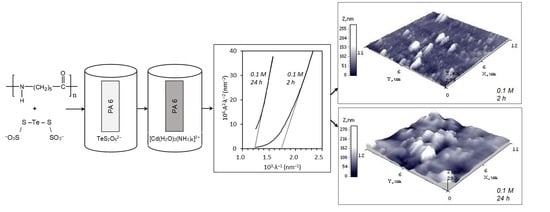
| Sample No | Molar Ratio Cd:Te:S | Direct bandgap Eg (eV) | R2 | Urbach Energy (eV) | R2 |
|---|---|---|---|---|---|
| S1*–2 | 1:4.3:5.4 | 2.36 | 0.9973 | 0.56 | 0.9993 |
| S1*–24 | 1:4.3:8.6 | 1.70 | 0.9995 | 0.62 | 0.9998 |
| S2*–2 | 1:5.2:13.0 | 2.15 | 0.9993 | 0.58 | 0.9997 |
| S2*–24 | 1:5.1:12.2 | 1.52 | 0.9946 | 0.66 | 0.9994 |
| Sample No | CdTe | CdS (JCPDS 80–6) | S8 (JCPDS 71–137) | ||||||||
|---|---|---|---|---|---|---|---|---|---|---|---|
| S2*-2 | S2*-24 | (JCPDS 80–89) | (JCPDS 15–770) | ||||||||
| 2θ | d (Å) | 2θ | d (Å) | d (Å) | h k l | d (Å) | h k l | d (Å) | h k l | d (Å) | h k l |
| 35.618 | 2.519 | 2.524 | 1 0 3 | ||||||||
| 38.444 | 2.340 | 38.444 | 2.340 | 2.439 | 1 0 2 | 2.341 | 1 4 2 | ||||
| 39.093 | 2.302 | 39.093 | 2.302 | 2.29 | 2 2 0 | 2.304 | 1 2 4 | ||||
| 40.789 | 2.210 | 40.789 | 2.210 | 2.213 | 3 2 3 | ||||||
| 45.331 | 1.999 | 45.331 | 1.999 | 1.991 | 1 1 2 | 1.954 | 3 1 1 | ||||
| 60.752 | 1.523 | 60.752 | 1.523 | 1.513 | 1 0 4 | ||||||
| Sample No | Max. Height, A (nm) | Average Height, Zmean (nm) | Average Roughness, Ra (nm) | RMS Roughness, Rq (nm) | Skewness, Rsk (nm) |
|---|---|---|---|---|---|
| Crude sample | 67.4 | 27.76 | 3.45 | 4.59 | 0.82 |
| S2*-2 | 279.2 | 62.04 | 20.09 | 29.97 | 1.26 |
| S2*-24 | 293.0 | 92.72 | 25.87 | 35.21 | 0.92 |
Publisher’s Note: MDPI stays neutral with regard to jurisdictional claims in published maps and institutional affiliations. |
© 2022 by the authors. Licensee MDPI, Basel, Switzerland. This article is an open access article distributed under the terms and conditions of the Creative Commons Attribution (CC BY) license (https://creativecommons.org/licenses/by/4.0/).
Share and Cite
Ivanauskas, R.; Samardokas, L.; Sukyte, J.; Zalenkiene, S.; Ancutiene, I. Structural and Optical Characterizations of Cadmium Chalcogenide Layers on Polyamide Formed Using Monotelluropentathionic Acid. Materials 2022, 15, 787. https://doi.org/10.3390/ma15030787
Ivanauskas R, Samardokas L, Sukyte J, Zalenkiene S, Ancutiene I. Structural and Optical Characterizations of Cadmium Chalcogenide Layers on Polyamide Formed Using Monotelluropentathionic Acid. Materials. 2022; 15(3):787. https://doi.org/10.3390/ma15030787
Chicago/Turabian StyleIvanauskas, Remigijus, Linas Samardokas, Judita Sukyte, Skirma Zalenkiene, and Ingrida Ancutiene. 2022. "Structural and Optical Characterizations of Cadmium Chalcogenide Layers on Polyamide Formed Using Monotelluropentathionic Acid" Materials 15, no. 3: 787. https://doi.org/10.3390/ma15030787