Article

Remarkable Reduction in IG with an Explicit Investigation of the Leakage Conduction Mechanisms in a Dual Surface-Modified Al2O3/SiO2 Stack Layer AlGaN/GaN MOS-HEMT

1
Department of Electrical Engineering, Institute of Microelectronics, National Cheng-Kung University, Tainan 701, Taiwan
2
Department of Electronic Engineering, I-Shou University, Kaohsiung 840, Taiwan
*
Author to whom correspondence should be addressed.
Materials 2022, 15(24), 9067; https://doi.org/10.3390/ma15249067
Submission received: 25 October 2022 / Revised: 25 November 2022 / Accepted: 14 December 2022 / Published: 19 December 2022
(This article belongs to the Special Issue Opto/Electronics Materials and Devices Applied for Telecommunications)

Abstract

:
We demonstrated the performance of an Al2O3/SiO2 stack layer AlGaN/GaN metal–oxide semiconductor (MOS) high-electron-mobility transistor (HEMT) combined with a dual surface treatment that used tetramethylammonium hydroxide (TMAH) and hydrochloric acid (HCl) with post-gate annealing (PGA) modulation at 400 °C for 10 min. A remarkable reduction in the reverse gate leakage current (IG) up to 1.5 × 10 12   A / mm (@ VG = −12 V) was observed in the stack layer MOS-HEMT due to the combined treatment. The performance of the dual surface-treated MOS–HEMT was significantly improved, particularly in terms of hysteresis, gate leakage, and subthreshold characteristics, with optimized gate annealing treatment. In addition, an organized gate leakage conduction mechanism in the AlGaN/GaN MOS–HEMT with the Al2O3/SiO2 stack gate dielectric layer was investigated before and after gate annealing treatment and compared with the conventional Schottky gate. The conduction mechanism in the reverse gate bias was Poole–Frankel emission for the Schottky-gate HEMT and the MOS–HEMT before annealing. The dominant conduction mechanism was ohmic/Poole-Frankel at low/medium forward bias. Meanwhile, gate leakage was governed by the hopping conduction mechanism in the MOS–HEMT without gate annealing modulation at a higher forward bias. After post-gate annealing (PGA) treatment, however, the leakage conduction mechanism was dominated by trap-assisted tunneling at the low to medium forward bias region and by Fowler–Nordheim tunneling at the higher forward bias region. Moreover, a decent product of maximum oscillation frequency and gate length (fmax × LG) was found to reach 27.16 GHz∙µm for the stack layer MOS–HEMT with PGA modulation. The dual surface-treated Al2O3/SiO2 stack layer MOS–HEMT with PGA modulation exhibited decent performance with an IDMAX of 720 mA/mm, a peak extrinsic transconductance (GMMAX) of 120 mS/mm, a threshold voltage (VTH) of −4.8 V, a higher ION/IOFF ratio of approximately 1.2 × 10 9 , a subthreshold swing of 82 mV/dec, and a cutoff frequency(ft)/maximum frequency of (fmax) of 7.5/13.58 GHz.

1. Introduction

Considering the unique features of III-nitride, e.g., high carrier density (~1013/cm3), large band gap (~3.4 eV), high saturation velocity (~ 2 × 10 7 cm/s), and large breakdown field (>3 MV/cm), extensive research has been conducted on AlGaN/GaN high-electron-mobility transistors (HEMTs) for high-power and high-frequency applications [1,2,3]. The high-density and high-mobility two-dimensional electron gas (2DEG) generated at the AlGaN/GaN interface enables us to understand how a power-switching transistor with low ON resistance is relevant to next-generation power conversion systems [4]. However, the performance of this type of transistor is inherently limited by high gate leakage current (IG) due to the strong polarization-induced electric field and Schottky gate contact [5]. The high gate leakage leads to a limited gate voltage swing (GVS), reduced radio frequency (RF) performance, and breakdown voltage (VBR).
Moreover, Cl2-based inductive coupled plasma (ICP) dry etching has been extensively used to isolate devices. This process correspondingly induces trap states in a device, leading to severe gate leakage current [6]. Lee et al. reported that surface conditions, e.g., the native oxide layer on the GaN surface or ICP etching damage, also severely affect device performance [7]. Thus, the native oxide layer or ICP etching damage must be removed from the surface to improve device performance. Numerous wet chemical solutions, including sulfuric acid (H2SO4), hydrogen fluoride (HF), hydrochloric acid (HCl), potassium hydroxide (KOH), and tetramethylammonium hydroxide (TMAH), have been used to improve the surface condition of devices [8,9,10,11,12,13,14,15]. Previous reports have suggested that TMAH surface treatment prior to gate oxide deposition can effectively enhance the performance of GaN HEMT devices to a considerable extent [7].
In addition to wet surface treatment, inserting a dielectric layer or stack structure under the metal gate can effectively suppress IG, improve current collapse, and provide better linearity [16]. Various dielectric materials, e.g., AlN [17], SiO2 [18], MgCaO [19], HfO2 [20], Al2O3 [21], HfAlOX [22], ZrO2 [23], and TiO2 [24], have been extensively investigated. Among these materials, Al2O3 is a potential candidate for fabricating a metal-oxide semiconductor (MOS)–HEMT due to its comparatively high dielectric constant (~9 eV), large bandgap (~6.5 eV) with a significant conduction band offset (~1.91 eV), and good interface with AlGaN [25,26]. However, to reduce the gate leakage current further and improve the conduction band offset, a thin layer of SiO2 with a larger bandgap (~9 eV) can be inserted under the Al2O3 layer [18]. Nevertheless, the interface traps between the stack gate dielectric (Al2O3/SiO2) and the (Al)GaN layer affect the performance of the MOS–HEMT. A previous report suggested that post-gate annealing (PGA) is an effective method for reducing the oxide defect charge, interface-trapped charge, and oxide-trapped charge [27].
To reduce IG further, and thus, improve device reliability and increase GVS, the gate leakage mechanism in AlGaN/GaN-based MOS–HEMTs before and after gate annealing should be investigated. Previous reports have indicated that Poole–Frankel emission (PFE), trap-assisted tunneling (TAT), and Fowler–Nordheim tunneling (FNT) are the dominant leakage mechanisms in the atomic layer deposition (ALD) of Al2O3/AlGaN/GaN and the low-power chemical vapor deposition (CVD) of the SiNx/AlGaN/GaN MOS–HEMT [28,29]. However, they have only investigated forward bias gate leakage characteristics. Although the forward and reverse leakage mechanisms of a SiNX MOS–HEMT were investigated previously in detail, the changes in the conduction mechanism after annealing were not considered [5]. To date, no report is available on the explicit investigation of the gate leakage conduction mechanism in a dual surface-treated Al2O3/SiO2 stack layer MOS–HEMT before and after gate annealing modulation.
With this objective, this work demonstrated the improved device performance with a remarkable reduction in the gate leakage current of a dual surface-treated Al2O3/SiO2 stack layer MOS–HEMT with PGA modulation. A detailed investigation of the conduction mechanism of gate leakage current in forward and reverse biases was performed on a MOS–HEMT before and after gate annealing treatment, and the results demonstrated how the dominant conduction mechanism was changed after PGA treatment. The dual surface-treated Al2O3/SiO2 stack layer MOS–HEMT with PGA modulation exhibited decent performance with a maximum drain current (IDMAX) of 720 mA/mm, a peak extrinsic transconductance (GMMAX)of 120 mS/mm, a threshold voltage (VTH) of −4.8 V, a higher ION/IOFF ratio of approximately 1.2 × 10 9 , a subthreshold swing (SS) of 82 mV/dec, and a cutoff frequency (ft)/maximum frequency (fmax) of 7.5/13.58 GHz, with the lowest gate leakage current of 1.5 × 10 12   A / mm and a decent (fmax × LG) of 27.16 GHz∙µm.

2. Materials and Methods

The AlGaN/GaN epitaxy was grown using a low-pressure metal-organic chemical vapour deposition (MOCVD) system on a p-type low-resistive (111) Si substrate. The epilayers consisted 3.9 µm GaN buffer layer, a 300 nm undoped GaN layer, a 20 nm Al0.25Ga0.75N barrier layer, and a 2 nm GaN cap layer. The measured sheet carrier concentration and Hall mobility were 6.15   ×   10 12 / cm 2 and 2338 cm 2 / V · s , respectively.
Device processing started with mesa isolation by using an ICP reactive ion etching system with a Cl2/BCl3 gas mixture. Then, the sample was immersed into 5% TMAH solution at 85 °C for 1 min to remove native oxide and ICP etching damage. Thereafter, the source and the drain regions were defined via ultraviolet (UV) photolithography. Then, Ti/Al/Ni/Au (25/150/30/120 nm) metal contacts were deposited using an electron beam (e-beam) evaporator system, followed by rapid thermal annealing at 875 °C for 30 s under N2 ambient atmosphere to ensure good ohmic contact. Subsequently, HCl wet treatment was performed for 3 min prior to gate metal deposition for conventional HEMT and gate oxide deposition for MOS-HEMT. Then, a stack gate dielectric layer composed of a 5 nm SiO2 followed by a 10 nm Al2O3 layer, was deposited using an ALD system (Picosun) at 250 °C. Finally, the gate region was defined via UV photolithography, and a Ni/Au (80/100 nm) gate stack was deposited using an e-beam evaporator followed by a liftoff process. To improve device performance further, PGA was performed at 400 °C for 10 min. Sheet resistance was 434 Ω/□. For reference, a MOS–HEMT with 5 nm SiO2 gate dielectric and a conventional HEMT were also fabricated. The gate width (WG) and gate length (LG) were 100 µm and 2 µm for all devices, and LGD and LSG were both 2 µm. To understand the gate annealing treatment on the MOS–HEMT and the conventional HEMT, all devices were fabricated following the same processing conditions without PGA treatment. Figure 1a,b shows the typical schematic of a MOS–HEMT and a planar HEMT. UV photolithography was performed using an MJB3 Karl Suss mask aligner system. DC I–V and RF performance were measured with a B1500A semiconductor characterization system and an Agilent N5245A network analyzer with an HP 4142B DC monitor, respectively. To understand the gate dielectric thickness we used transmission electron microscopy (TEM) (JEOL JEM-2100F) system. After the focused ion beam, we used carbon lacey grid for better resolution of the TEM image. To understand the quantitative analysis of the surface composition and material elemental composition we did X-ray photoelectron spectroscopy (XPS) (JEOL). To analyze the effect of TMAH wet surface treatment on the performance of the stack layer MOS–HEMT device, XPS was conducted using a k-alpha X-ray photoelectron spectrometer. To stick the sample on the holder for XPS a copper foil conductive has been used. A monochromatic Al Kα X-ray source with 90° taken off-angle was used. The sputtering depth was approximately 30–50 nm.

3. Results

Figure 1c,d shows the TEM image of the Al2O3/SiO2 MOS–HEMT before and after gate annealing treatment. Clear layers of the 5 nm SiO2 and 10 nm Al2O3 were found without intermixing before PGA treatment. Owing to the diffusion of atoms, a less layered structure was observed after gate annealing treatment. Typical atomic force microscopy (AFM) images are shown in Figure 2a–e under different conditions. As shown in Figure 2a,b, side wall surface morphology was improved with TMAH surface treatment. After dual surface treatment with PGA modification, the root-mean-square roughness was significantly improved from 0.70 nm to 0.24 nm, subsequently enhancing device performance.
Figure 3 illustrates the change in the atomic composition of the Ga 3 core levels before and after surface treatment, with both spectra deconvoluted into two peaks of Ga-N and Ga-O. The Ga 3d5/2 and Ga2O3 (Ga3+) peaks were de-convoluted by considering spin-orbital splitting [30]. Figure 3 clearly shows that the intensity of Ga-O is considerably lower after TMAH surface treatment. The peak intensity ratio of Ga-O/Ga-N significantly decreased to 6.6% from 63%. The removal of native oxide at the GaN surface via wet surface treatment reduced the intensity of the Ga-O bond, subsequently improving device performance as previously reported [31,32,33,34].
The typical drain current versus voltage (ID–VD) characteristics of the conventional HEMT and the Al2O3/SiO2 stack layer MOS–HEMT are shown in Figure 4. The IDMAX of the dual surface-treated stack layer (SiO2) MOS–HEMT and the conventional HEMT was 720 mA/mm (650 mA/mm) (@ VG = 3 V) and 520 mA/mm (@ VG = 1 V), respectively, with PGA modulation, as shown in Figure 4. Better pinch-off behavior in the stack layer MOS–HEMT suggested better gate controllability than in the SiO2 MOS–HEMT. The conventional HEMT was not biased with higher VG due to the large late leakage current. The reduction of IDMAX in the conventional HEMT was attributed to the large IG [35]. Moreover, IDMAX was 650 mA/mm (500 mA/mm) for the MOS–HEMT (HEMT) without annealing modulation. In addition, the ON resistance (RON) was significantly reduced from 6.3 Ω.mm to 4.9 Ω.mm in the MOS–HEMT due to dual surface treatment with the application of a stack dielectric layer.
The transfer characteristics of the stack layer MOS–HEMT and the conventional HEMT before and after gate annealing treatment (@ VD = 4 V) are shown in Figure 5. The Al2O3/SiO2 stack layer MOS–HEMT exhibited a VTH of −4.8 V (−4.4 V) with (without) gate annealing modulation. For the conventional HEMT and the SiO2 MOS–HEMT, VTH was −2.7 V and −3.6 V, respectively. The threshold voltage is defined as the gate bias intercept point of the linear extrapolation of the drain current at GMMAX [22]. The VTH difference between HEMT and MOS–HEMT can be expressed as [5]:
V TH , MOS HEMT     V TH , HEMT   = ( Q i n t ε o x ) · t o x ( q n o x 2 ε o x ) · t o x 2 ,
where Qint is the total interface charge, tox is the thickness of the dielectric layer, ε o x is the effective dielectric constant of the stack dielectric layer, and nox is the oxide bulk charge. In accordance with Equation (1), the negative shift of VTH is attributable to the increment of the interface fixed charge at the interface and oxide layers and the increase in the 2DEG concentration after passivation [36,37,38]. Moreover, the increase in separation between the gate and the channel layer may be another reason for the negative shifting of VTH. The shift of VTH to the reverse direction with gate annealing treatment was confirmed in Figure 5b.
An improvement in peak extrinsic transconductance (GMMAX) was observed in the dual surface-treated Al2O3/SiO2 stack layer MOS–HEMT after gate annealing modulation compared with the SiO2 MOS–HEMT or the conventional HEMT shown in Figure 5. The GMMAX values were 120 mS/mm (102 mS/mm) and 123 mS/mm (110 mS/mm) in the stack layer MOS–HEMT and the conventional HEMT with annealing (without annealing) modulation. The insertion of the two gate dielectrics increased the distance between the gate and the 2DEG channel, reducing gate controllability and decreasing GMMAX in MOS–HEMT. In addition, GVS, defined as the 10% drop in maximum transconductance, was calculated for both devices to understand the linearity behavior of the device [20]. GVS improved from 1.10 V to 1.92 V in the dual surface-treated stack layer MOS–HEMT after gate annealing treatment. Thus, low phase noise, device linearity, and wide dynamic range were improved after dual surface treatment and PGA modulation in the stack layer MOS–HEMT [39]. Moreover, GMMAX was 91 mS/mm in the SiO2 MOS–HEMT.
Figure 6 shows the subthreshold characteristics as a function of gate voltage (@ VD = 4 V) for all devices. In this figure, the subthreshold drain leakage current was decreased by more than three orders of magnitude in the Al2O3/SiO2 MOS–HEMT after gate annealing modulation compared with that of the conventional HEMT. The subthreshold drain leakage current was influenced by the reverse bias gate leakage current in the pinch-off region [39]. Given that IG was suppressed by the combined effects of the stack layer gate dielectric and dual surface treatment with PGA modulation in MOS–HEMT, as discussed later, the subthreshold drain leakage current was decreased to a considerable extent. Subthreshold swing (SS) also depends on IG. The SS values of different devices were extracted from Figure 6. The SS values were improved from 130 mV/dec to 82 mV/dec in the stack layer MOS–HEMT after gate annealing treatment. Meanwhile, for the conventional HEMT (SiO2 MOS–HEMT), the SS value was 178 mV/dec (91 mV/dec). The current ON/OFF (ION/IOFF) ratios were 1.2 × 10 9 and 5.8 × 10 7 for the stack layer MOS–HEMT with and without PGA treatment. By contrast, no significant improvement in the current ratio was found in the planar HEMT after gate annealing treatment.
The reverse and forward gate leakage current (IG–VG) characteristics of the dual surface-treated stack layer MOS–HEMT before and after gate annealing treatment and the Schottky gate HEMT without PGA were measured, and the results are presented in Figure 7. The reverse gate leakage current (@ VG = −12 V) of the Al2O3/SiO2 MOS–HEMT was 2.3 × 10 8   A / mm before gate annealing treatment. Evidently, IG was significantly reduced by four orders of magnitude to 1.5 × 10 12   A / mm after annealing treatment with dual surface modification. The insertion of large bandgap materials as gate dielectric combined with dual surface treatment and PGA modulation reduced IG to a considerable extent.
To explore the charge of transportation mechanisms responsible for the gate leakage phenomenon, IG–VG characteristics were divided into five regions as indicated in Figure 7. Leakage characteristics were analyzed in different regions to determine the dominant leakage mechanism for each particular region. The multiple conduction mechanism was studied to justify the appropriate charge transport phenomenon in the stack layer MOS–HEMT before and after gate annealing treatment and conventional HEMT. The conduction band edge diagram of the MOS–HEMT before and after PGA treatment and HEMT under different operating regions that illustrated the conduction mechanisms is shown in Figure 8.

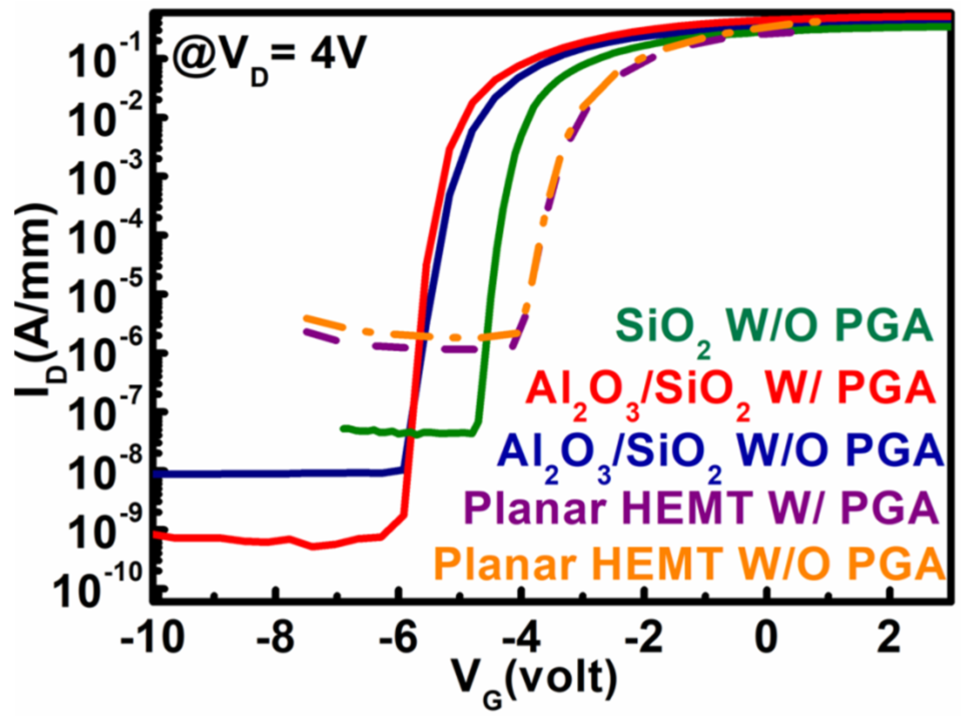
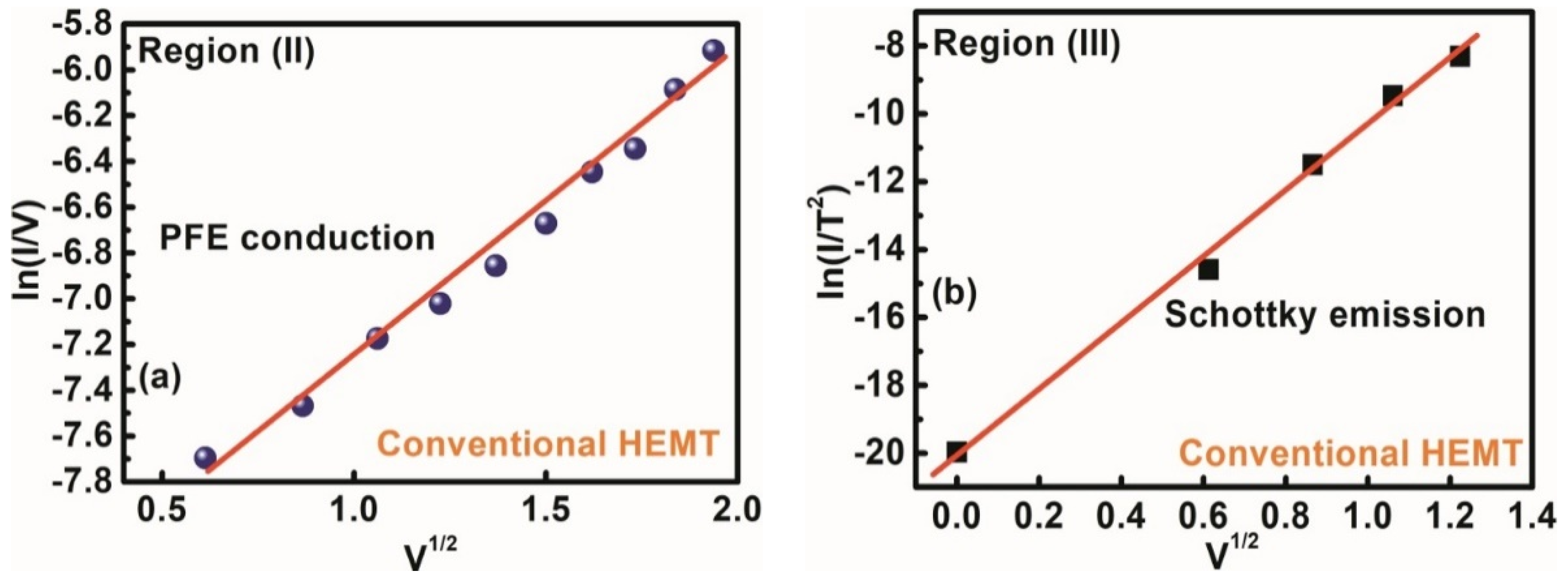
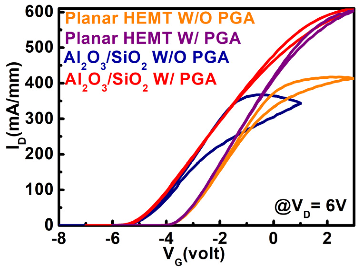
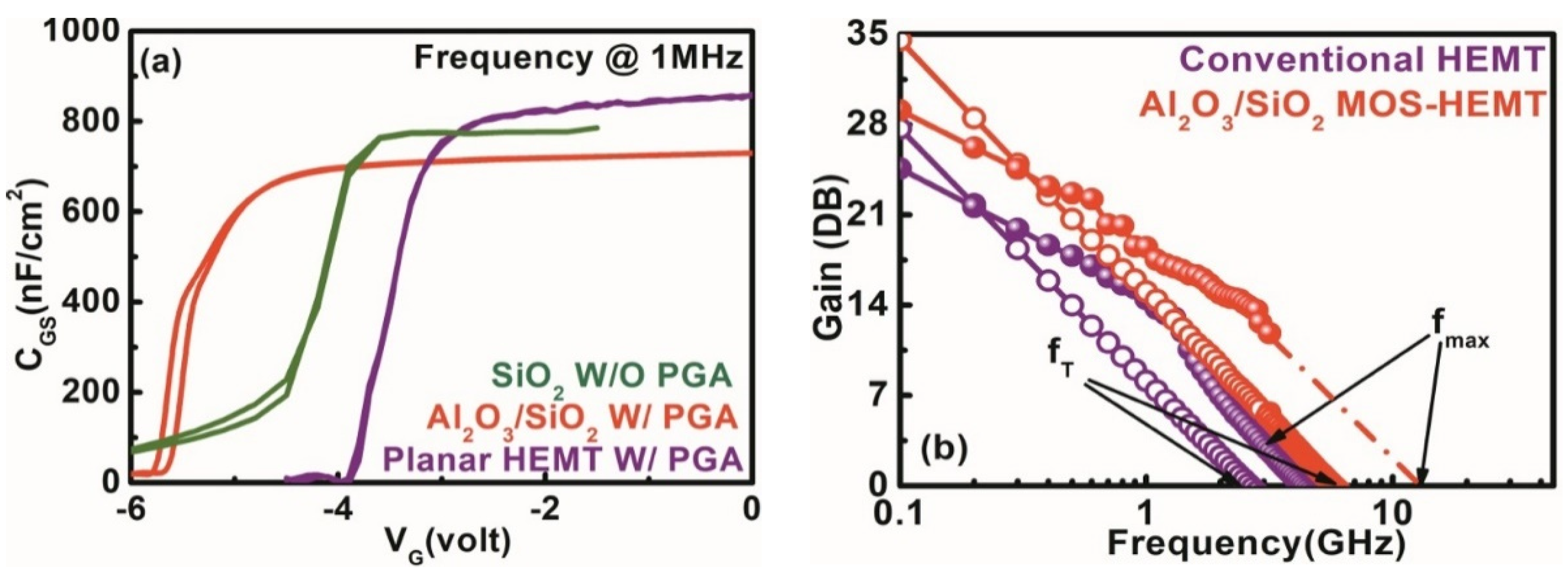
3.1. Gate Leakage Mechanisms in the AlGaN/GaN MOS–HEMT before Gate Annealing

For the stack layer MOS–HEMT before annealing treatment, as indicated in Region (I) for VG   VTH, the leakage current was saturated due to the saturation of the vertical electrical fields across the gate dielectric and the barrier layer [5]. However, the IG–VG characteristics in Region (II) exhibited dependency on the applied electric field, and the PFE mechanism clearly dominated this region, as suggested in the fitted curve of [ln (I/V) vs V1/2] in Figure 9a. A comparatively high electric field supported the PFE conduction depicted in the fitted Figure 9a, and the charge transferred through a trap shown in the band edge diagram in Figure 8a in this region exhibited the following relation [5,40]:
  ln ( J P F E E D i ) = m E D i + c
m = q k T q π ε D i
where ε D i is the permittivity of the dielectric materials, kB is the Boltzmann’s constant, T is the temperature, and q is the electronic charge. The effective dielectric constant (ɛDi) was extracted to 7.2 from the ln (I/V) vs V1/2 characteristics, which was sufficiently close to the calculated effective dielectric constant of the Al2O3/SiO2 layer [41].
The dominant leakage conduction mechanism in Region (III) was ohmic due to the linear relationship of ln (I) vs. ln (V), with a slope value close to 1, as shown in Figure 9b. The leakage mechanism was assumed to be PFE at a comparatively higher voltage region. The linear fitting in Figure 9c further confirmed PFE conduction because electrons can be de-trapped with an increased electric field as shown in the band edge diagram in Figure 8b. In addition, the dominant conduction mechanism in a high field region (VG 3 V) was satisfied with hopping conduction from the fitted curve of ln (I) vs. V, as shown in Figure 9d. Hopping distance ( λ ) can be extracted from the fitted curve by considering the following equation [40,42]:
J = q n λ   e x p ( q λ E E a k T )
where n is the electron concentration, f is the thermal vibration frequency of the trapping sites, E is the corresponding electric field, and Ea is the activation energy. The hopping distance was calibrated to 0.47 nm by using Equation (4). The electrons can overcome the hopping distance ( λ ) in the higher field region, as shown in Figure 8c, due to the higher energy.

3.2. Gate Leakage Mechanisms in the AlGaN/GaN MOS–HEMT after Gate Annealing

The leakage mechanism of the Al2O3/SiO2 MOS–HEMT after gate annealing modulation was also investigated as shown in Figure 10. After gate annealing modulation, shallow traps were reduced [39] and IG was independent of gate voltage at VG 2 V due to the saturation of the electric field [5]. The conduction band diagram in Region (IV) for the stack layer MOS–HEMT after annealing treatment is shown in Figure 8d. In this region, leakage transportation was estimated from the fitting curve of [ln (I) vs. 1/V], as shown in Figure 10a, to a two-step TAT mechanism. The electric field dependence of the TAT current (JTAT) is given by the following equation [43]:
  J T A T = A e x p ( 8 π 2 q m T 3 3 h E )
where T is the trapped energy of electron traps with respect to the conduction band edge, A is a constant, and h is Planck’s constant. Shallow traps were reduced through the creation of deep traps via PGA modulation, causing the conduction mechanism to shift toward TAT from PFE after gate annealing treatment as indicated in the band diagram of TAT in Figure 8d [44].
Consequently, the leakage mechanism in the high forward bias region was dominated by FNT across the Al2O3/SiO2 gate dielectric layer, as shown in Figure 10b. FNT current density (JFNT) can be related to the electric field across the dielectric (EDi) by [45]:
ln ( J F N T E D i 2 ) = l n   ( A ) B | E D i |
where A is a constant, B = 8 π (2 mn*(q e f f )3)1/2/(3qh), mn* is the effective mass of the electron in the gate dielectric, e f f is the effective barrier height of the electrons for FNT, and h is Planck’s constant. The linear relationship of the ln ( I V 2 )   vs .   1 / V graph in Figure 10b verified the FNT conduction mechanism in Region (V) for the MOS–HEMT after gate annealing modulation. The band edge diagram of FNT is shown in Figure 8e.

3.3. Gate Leakage Mechanisms in the AlGaN/GaN HEMT

We also investigated the conduction mechanism of leakage current in the conventional HEMT without PGA by dividing the IG–VG characteristics into different regions, as shown in Figure 7. From Figure 7, IG (@ VG −4 V) was clearly saturated due to the saturation of the vertical electrical fields as mentioned previously. The conduction mechanism in Region (II) was confirmed as PFE conduction from the ln (I/V) vs. V1/2 graph by following Equation (2), similar to the stack layer MOS–HEMT before PGA treatment, as shown in Figure 11a. In addition, Schottky emission (SE) dominated Region (III) with increasing electric fields at VG > 0 from the linear slope of ln (I/T2) vs. V1/2, as shown in Figure 11b, in accordance with the following relation [7]:
I G = A T 2 e x p ( B k T ) e x p ( S S E V k T d )
S S E = 1 2 ( q 3 π ε 0 ε r ) 1 2
where S S E is the SE lowering coefficients, and B is the Schottky barrier height as depicted in the conduction band edge of Region (III) in Figure 8f. In general, SE leads to conduction through the contact interface rather than from bulk material. By contrast, PFE is closely related to the tunneling of carriers and associated with the wide distribution of traps in the band gap of dielectric materials, which originates from impurities and/or structural defects.
To understand the interface quality of the devices, the hysteresis characteristics of the Al2O3/SiO2 stack layer MOS–HEMT and the conventional MOS–HEMT were measured (@ VG = 6 V) before and after gate annealing treatment, as shown in Figure 12. Hysteresis behavior was significantly improved after gate annealing modulation in both devices. After gate annealing modulation, the MOS–HEMT exhibited nearly low hysteresis of 0.1 V due to the affective neutralization of the surface caused by the combined effects of TMAH/HCl surface treatment with gate annealing modulation [7]. In addition, a counterclockwise hysteresis was observed in both devices. No surface states were available to capture electrons at a high gate voltage due to the presence of acceptor-like surface states, and electron density in the 2DEG channel was increased to raise the channel current, resulting in counterclockwise hysteresis [7,46].
To understand the reduction of trap states after dual surface treatment and PGA modulation with the stack layer gate dielectric in the MOS–HEMT compared with that in the conventional HEMT, capacitance-voltage (C–V) measurements were performed at 1 MHz for both devices as shown in Figure 13a. The high-frequency performance of the stack layer MOS–HEMT and the conventional HEMT without PGA, and short-circuit current gain ( | H 21 | ), maximum stable gain/maximum available gain (MSG/MAG) were measured as shown in Figure 13b. The measured cut-off frequency (ft) and maximum oscillation frequency (fmax) of the MOS–HEMT were 7.5 GHz and 13.5 GHz, while those for the conventional HEMT were only 2.7 GHz and 5 GHz, respectively. The comparatively higher (fmax × LG) was recorded in the MOS–HEMT after PGA modification in contrast with previous reports as indicated in Table 1. The interface state density (Dit) for the dual surface-treated MOS–HEMT can be extracted from a previously reported formula [47] to be 1.61 × 10 12   eV 1 cm 2 , which is significantly improved from that of the conventional HEMT ( 1.1 × 10 13   eV 1 cm 2 ) . For the SiO2 MOS–HEMT, Dit was 3.8 × 10 12   eV 1 cm 2 . Given the combined effects of dual surface treatment and the stack dielectric layer with gate annealing modulation, Dit was significantly reduced up to one order of magnitude lower in the MOS–HEMT compared with that in the conventional HEMT. Table 1 presents the DC performance and high-frequency comparison of the different gate structure MOS–HEMTs, including the PGA modulated dual surface-treated Al2O3/SiO2 stack layer MOS–HEMT [17,19,31,48,49,50,51].

4. Conclusions

In summary, we successfully demonstrated the performance of an Al2O3/SiO2 stack layer MOS–HEMT that used TMAH and HCl dual surface treatment prior to gate oxide deposition with PGA modulation. The off-state gate leakage current was remarkably reduced to 1.5 × 10 12   A / mm , which was seven orders of magnitude lower (~10−5 A/mm) than that of the conventional HEMT. A significant reduction in IG was observed in MOS–HEMT due to the combined effects of dual surface treatment and the stack gate dielectric layer with gate annealing modulation at 400 °C. In addition, a systematic investigation of the gate leakage conduction mechanism of the conventional HEMT and the MOS–HEMT before and after PGA modulation was conducted. At reverse bias, the PFE conduction mechanism dominated both devices. At low and medium forward bias, the dominant conduction mechanisms were ohmic and PFE, and at higher forward bias, gate leakage was governed by the hopping conduction mechanism for the MOS–HEMT before PGA. By contrast, after the gate annealing treatment of MOS–HEMT, the dominant leakage conduction mechanism was TAT at the low to medium forward bias region and FNT at the higher forward bias region due to the reduction of shallow traps.

Author Contributions

S.M. was responsible for the device preparation, characterization, modeling discussion and writing the draft. P.P. was responsible for the characterization and modeling discussion; K.-W.L. was responsible for the data analysis and editing of the manuscript; Y.-H.W. was the advisor who supervised the progress and paper editing. All authors have read and agreed to the published version of the manuscript.

Funding

This research was funded by the Ministry of Science and Technology, Taiwan, grant numbers MOST 106-2221-E-006-219-MY3 and MOST 109-2221-E-06-075-MY2; Transcom Inc., Taiwan, grant number 109S0172; and Materials Analysis Technology Inc. under Contract No. 2021-T-01.

Institutional Review Board Statement

Not applicable.

Informed Consent Statement

Not applicable.

Data Availability Statement

The data presented in this study are available on request from the corresponding author.

Acknowledgments

The authors acknowledge the use of the TEM, EDS, and ALD systems belonging to the core facility center of National Cheng-Kung University, Tainan, Taiwan. Taiwan Semiconductor Research Institute of National Applied Research Laboratories, Taiwan for the support of high-frequency measurements and device characterization are also highly appreciated.

Conflicts of Interest

The authors declare no conflict of interest.

References

  1. Borga, M.; Meneghini, M.; Benazzi, D.; Canato, E.; Püsche, R.; Derluyn, J.; Abid, I.; Medjdoub, F.; Meneghesso, G.; Zanoni, E. Buffer breakdown in GaN-on-Si HEMTs: A comprehensive study based on a sequential growth experiment. Microelectron. Reliab. 2019, 100–101, 113461. [Google Scholar] [CrossRef]
  2. Ardaravĭcius, L.; Matulionis, A.; Liberis, J.; Kiprijanovic, O.; Ramonas, M.; Eastman, L.F.; Shealy, J.R.; Vertiatchikh, A. Electron drift velocity in AlGaN/GaN channel at high electric fields. Appl. Phys. Lett. 2003, 83, 4038–4040. [Google Scholar] [CrossRef]
  3. Mazumder, S.; Wang, Y.H. Investigation of HfSiOX passivation effect on AlGaN/GaN HEMT. In Proceedings of the 2020 International Symposium on Devices, Circuits and Systems, ISDCS, Howrah, India, 4–6 March 2020; pp. 1–4. [Google Scholar]
  4. Hori, Y.; Yatabe, Z.; Hashizume, T. Characterization of interface states in Al2O3/AlGaN/GaN structures for improved performance of high-electron-mobility transistors. J. Appl. Phys. 2013, 114, 244503. [Google Scholar] [CrossRef] [Green Version]
  5. Dutta, G.; DasGupta, N.; DasGupta, A. Gate Leakage Mechanisms in AlInN/GaN and AlGaN/GaN MIS-HEMTs and Its Modelling. IEEE Trans. Electron Devices 2017, 64, 3609–3615. [Google Scholar] [CrossRef]
  6. Jun, L.; Lei, Z.S.; Han, M.M.; Bin, H.; Lei, Y.X.; Cheng, Z.J.; Hua, M.X.; Yue, H. Trap states induced by reactive ion etching in AlGaN/GaN high-electron-mobility transistors. Chin. Phys. B 2015, 24, 117305. [Google Scholar]
  7. Reddy, M.S.P.; Park, W.S.; Im, K.S.; Lee, J.H. Dual-surface modification of AlGaN/GaN HEMTs using TMAH and piranha solutions for enhancing current and 1/f-Noise Characteristics. IEEE J. Electron Devices Soc. 2018, 6, 791–796. [Google Scholar] [CrossRef]
  8. Eller, B.S.; Yang, J.; Nemanich, R.J. Electronic surface and dielectric interface states on GaN and AlGaN. J. Vac. Sci. Technol. A 2013, 31, 050807. [Google Scholar] [CrossRef]
  9. Koyama, Y.; Hashizume, T.; Hasegawa, H. Formation processes and properties of Schottky and ohmic contacts on n-type GaN for field effect transistor applications. Solid State Electron. 1999, 43, 1483–1488. [Google Scholar] [CrossRef]
  10. Rickert, K.A.; Ellis, A.B.; Himpsel, F.J.; Sun, J.; Kuech, T.F. n-GaN surface treatments for metal contacts studied via X-ray photoemission spectroscopy. Appl. Phys. Lett. 2002, 80, 204–206. [Google Scholar] [CrossRef] [Green Version]
  11. Hashizume, T.; Ootomo, S.; Oyama, S.; Konishi, M.; Hasegawa, H. Chemistry and electrical properties of surfaces of GaN and GaN/AlGaN heterostructures. J. Vac. Sci. Technol. B 2001, 19, 1675–1681. [Google Scholar] [CrossRef] [Green Version]
  12. Nepal, N.; Garces, N.Y.; Meyer, D.J.; Hite, J.K.; Mastro, M.A.; Eddy, C.R., Jr. Assessment of GaN surface pre-treatment for atomic layer deposited high-k dielectrics. Appl. Phys. Exp. 2011, 4, 055802. [Google Scholar] [CrossRef]
  13. Ganguly, S.; Verma, J.; Hu, Z.; Xing, H.; Jena, D. Performance enhancement of InAlN/GaN HEMTs by KOH surface treatment. Appl. Phys. Exp. 2014, 7, 034102. [Google Scholar] [CrossRef]
  14. Zhuang, D.; Edgar, J.H. Wet etching of GaN, AlN, and SiC: A review. Mater. Sci. Eng. R Rep. 2005, 48, 1–46. [Google Scholar] [CrossRef]
  15. Son, D.H.; Jo, Y.W.; Won, C.H.; Lee, J.H.; Seo, J.H.; Lee, S.H.; Lim, J.W.; Kim, J.H.; Kang, I.M.; Cristoloveanu, S.; et al. Normally-off AlGaN/GaN-based MOS-HEMT with self-terminating TMAH wet recess etching. Solid State Electron. 2018, 141, 7–12. [Google Scholar] [CrossRef]
  16. Lee, K.W.; Chou, D.W.; Wu, H.R.; Huang, J.J.; Wang, Y.H.; Houng, M.P.; Chang, S.J.; Su, Y.K. GaN MOSFET with liquid phase deposited oxide gate. Electron. Lett. 2002, 38, 829–830. [Google Scholar] [CrossRef]
  17. Tsurumi, N.; Ueno, H.; Murata, T.; Ishida, H.; Uemoto, Y.; Ueda, T.; Inoue, K.; Tanaka, T. AlN passivation over AlGaN/GaN HFETs for surface heat spreading. IEEE Trans. Electron Devices 2010, 57, 980–985. [Google Scholar] [CrossRef]
  18. Mazumder, S.; Li, S.H.; Wu, Z.G.; Wang, Y.H. Combined Implications of UV/O3 Interface Modulation with HfSiOX Surface Passivation on AlGaN/AlN/GaN MOS-HEMT. Crystals 2021, 11, 136. [Google Scholar] [CrossRef]
  19. Zhou, H.; Lou, X.; Sutherlin, K.; Summers, J.; Kim, S.B.; Chabak, K.D.; Gordon, R.G.; Ye, P.D. DC and RF Performance of AlGaN/GaN/SiC MOSHEMTs With Deep Sub-Micron T-Gates and Atomic Layer Epitaxy MgCaO as Gate Dielectric. IEEE Electron Device Lett. 2017, 38, 1409–1412. [Google Scholar] [CrossRef]
  20. Yue, Y.; Hao, Y. AlGaN/GaN MOS-HEMT with HfO2 Dielectric and Al2O3 Interfacial Passivation Layer Grown by Atomic Layer Deposition. IEEE Electron Device Lett. 2008, 29, 838–840. [Google Scholar] [CrossRef]
  21. Dutta, G.; DasGupta, N.; DasGupta, A. Effect of Sputtered-Al2O3 Layer Thickness on the Threshold Voltage of III-Nitride MIS-HEMTs. IEEE Trans. Electron Devices 2016, 63, 1450–1458. [Google Scholar] [CrossRef]
  22. Yang, S.K.; Mazumder, S.; Wu, Z.G.; Wang, Y.H. Performance enhancement in N2 plasma modified AlGaN/AlN/GaN MOS-HEMT using HfAlOX gate dielectric with Γ-shaped gate engineering. Materials 2021, 14, 1534. [Google Scholar] [CrossRef] [PubMed]
  23. Byun, Y.C.; Lee, J.G.; Meng, X.; Lee, J.S.; Lucero, A.T.; Kim, S.J.; Young, C.D.; Kim, M.J.; Kim, J. Low temperature (100 °C) atomic layer deposited-ZrO2 for recessed gate GaN HEMTs on Si. Appl. phys. Lett. 2017, 111, 082905. [Google Scholar] [CrossRef]
  24. Wu, T.Y.; Lin, S.K.; Sze, P.W.; Huang, J.J.; Chien, W.C.; Hu, C.C.; Tsai, M.J.; Wang, Y.H. AlGaN/GaN MOSHEMTs with liquid-phase deposited TiO2 as gate dielectric. IEEE Trans. Electron Devices 2009, 56, 2911–2916. [Google Scholar] [CrossRef]
  25. Hashizume, T.; Ootomo, S.; Hasegawa, H. Suppression of current collapse in insulated gate AlGaN/GaN heterostructure field-effect transistors using ultrathin Al2O3 dielectric. Appl. Phys. Lett. 2003, 83, 2952–2954. [Google Scholar] [CrossRef] [Green Version]
  26. Rawat, A.; Meer, M.; Surana, V.K.; Bhardwaj, N.; Pendem, V.; Garigapati, N.S.; Yadav, Y.; Ganguly, S.; Saha, D. Thermally Grown TiO2 and Al2O3 for GaN-Based MOS-HEMTs. IEEE Trans. Electron Devices 2018, 65, 3725–3731. [Google Scholar] [CrossRef]
  27. Liu, H.Y.; Ou, W.C.; Hsu, W.C. Investigation of post oxidation annealing effect on H2O2-Grown Al2O3/AlGaN/GaN MOS-HEMTs. IEEE J. Electron Devices Soc. 2016, 4, 358–364. [Google Scholar] [CrossRef]
  28. Liu, Z.H.; Ng, G.I.; Arulkumaran, S.; Maung, Y.K.T.; Zhou, H. Temperature-dependent forward gate current transport in atomic layer-deposited Al2O3/AlGaN/GaN metal-insulator-semiconductor high electron mobility transistor. Appl. Phys. Lett. 2011, 98, 163501-1–163501-3. [Google Scholar] [CrossRef]
  29. Hua, M.; Liu, C.; Yang, S.; Liu, S.; Fu, K.; Dong, Z.; Cai, Y.; Zhang, B.; Chen, K.J. Characterization of leakage and reliability of SiNXgate dielectric by low-pressure chemical vapor deposition for GaN based MIS-HEMTs. IEEE Trans. Electron Devices 2015, 62, 3215–3222. [Google Scholar] [CrossRef]
  30. Mazumder, S.; Pal, P.; Tsai, T.J.; Lin, P.C.; Wang, Y.H. A low program voltage enabled flash like AlGaN/GaN stack layered MIS-HEMTs using trap assisted technique. ECS J. Solid State Sci. Technol. 2021, 10, 055019. [Google Scholar] [CrossRef]
  31. Wang, C.; Chen, Y.C.; Hsu, H.T.; Tsao, Y.F.; Lin, Y.C.; Dee, C.F.; Chang, E.Y. Adoption of the Wet Surface Treatment Technique for the Improvement of Device Performance of Enhancement-Mode AlGaN/GaN MOS-HEMTs for Millimeter-Wave Applications. Materials 2021, 14, 6558. [Google Scholar] [CrossRef]
  32. Do, J.W.; Jung, H.W.; Shin, M.J.; Ahn, H.K.; Kim, H.; Kim, R.H.; Cho, K.J.; Chang, S.J.; Min, B.G.; Yoon, H.S.; et al. The effects of tetramethylammonium hydroxide treatment on the performance of recessed-gate AlGaN/GaN high electron mobility transistors. Thin Solid Film. 2017, 628, 31–35. [Google Scholar] [CrossRef]
  33. Sharma, P.; Sundaram, M.M.; Singh, D.; Ahuja, R. Highly Energetic and Stable Gadolinium/Bismuth Molybdate with a Fast Reactive Species, Redox Mechanism of Aqueous Electrolyte. ACS Appl. Energy Mater. 2020, 3, 12385–12399. [Google Scholar] [CrossRef]
  34. Manickam, M.; Singh, P.; Issa, T.B.; Thurgate, S.; Marco, R.D. Lithium insertion into manganese dioxide electrode in MnO2/Zn aqueous battery: Part I. A preliminary study. J. Power Source 2004, 130, 254–259. [Google Scholar] [CrossRef]
  35. Zheng, Y.Y.; Yue, H.; Cheng, Z.J.; Qian, F.; Yu, N.J.; Hua, M.X. A study on Al2O3 passivation in GaN MOS- HEMT by pulsed stress. Chin. Phys. B 2008, 17, 1405–1409. [Google Scholar] [CrossRef]
  36. Vetury, R.; Zhang, N.Q.; Keller, S.; Mishra, U.K. The impact of surface states on the DC and RF characteristics of AlGaN/GaN HFETs. IEEE Trans. Electron Devices 2001, 48, 560–566. [Google Scholar] [CrossRef]
  37. Liu, C.; Chor, E.F.; Tan, L.S. Improved DC performance of AlGaN/GaN high electron mobility transistors using hafnium oxide for surface passivation. Thin Solid Film. 2007, 515, 4369–4372. [Google Scholar] [CrossRef]
  38. Ozaki, S.; Makiyama, K.; Ohki, T.; Okamoto, N.; Kumazaki, Y.; Kotani, J.; Kaneki, S.; Nishiguchi, K.; Nakamura, N.; Hara, N.; et al. Improved DC performance and current stability of ultrathin-Al2O3/InAlN/GaN MOSHEMTs with post-metallization-annealing process. Semicond. Sci. Technol. 2020, 35, 035027. [Google Scholar] [CrossRef]
  39. Mazumder, S.; Wu, Z.G.; Pan, P.C.; Li, S.H.; Wang, Y.H. DC performance improvement of nanochannel AlGaN/AlN/GaN HEMTs with reduced OFF-state leakage current by post-gate annealing modulation. Semicond. Sci. Technol. 2021, 36, 095003. [Google Scholar] [CrossRef]
  40. Sze, S.M.; Ng, K.K. Physics of Semiconductor Devices, 3rd ed.; Springer Science & Business Media: Berlin, Germany, 2006. [Google Scholar]
  41. Sareni, B.; Krahenbuhl, L.; Beroual, A.; Brosseau, C. Effective dielectric constant of random composite materials. J. Appl. Phys. 1997, 81, 2375–2383. [Google Scholar] [CrossRef] [Green Version]
  42. Pal, P.; Mazumder, S.; Huang, C.W.; Lu, D.D.; Wang, Y.H. Impact of Barrier Layer on High Thermal and Mechanical Stability of a Flexible Resistive Memory in Neural Network Application. ACS Appl. Electron. Mater. 2021, 4, 1072–1081. [Google Scholar] [CrossRef]
  43. Wang, Q.; Periasamy, K.; Fu, Y.; Chan, Y.T.; Tan, C.M.; Bajalovic, N.; Wang, J.C.; Loke, D.K. Analytical modeling electrical conduction in resistive-switching memory through current-limiting-friendly combination frame works. AIP Adv. 2020, 10, 085117. [Google Scholar] [CrossRef]
  44. Kim, H.; Lee, J.; Liu, D.; Lu, W. Gate current leakage and breakdown mechanism in unpassivated AlGaN/GaN high electron mobility transistors by post-gate annealing. Appl. Phys. Lett. 2005, 86, 143505. [Google Scholar] [CrossRef]
  45. Turuvekere, S.; Karumuri, N.; Rahman, A.A.; Bhattacharya, A.; Dasgupta, A.; DasGupta, N. Gate leakage mechanisms in AlGaN/GaN and AlInN/GaN HEMTs: Comparison and modeling. IEEE Trans. Electron Devices 2013, 60, 3157–3165. [Google Scholar] [CrossRef]
  46. Chikhaoui, W.; Bluet, J.M.; Bru-Chevallier, C.; Dua, C.; Aubry, R. Deep traps analysis in AlGaN/GaN heterostructure transistor. Phys. Status Solidi C 2010, 7, 92–95. [Google Scholar] [CrossRef]
  47. Mazumder, S.; Wu, Z.G.; Wang, Y.H. Positive Shifting of Vth with Enhanced DC Performance in AlGaN/GaN Schottky-Gate HEMT through Optimized UV/O3 Treated Gate Interface and Thermal Engineering. ECS J. Solid State Electron. 2022, 11, 065002. [Google Scholar] [CrossRef]
  48. Shi, Y.T.; Xu, W.Z.; Zeng, C.K.; Ren, F.F.; Ye, J.D.; Zhou, D.; Chen, D.J.; Zhang, R.; Zheng, Y.; Lu, H. High-k HfO2-Based AlGaN/GaN MIS-HEMTs With Y2O3 Interfacial Layer for High Gate Controllability and Interface Quality. IEEE J. Electron Devices Soc. 2019, 8, 15–19. [Google Scholar] [CrossRef]
  49. Chou, B.Y.; Hsu, W.C.; Liu, H.Y.; Lee, C.S.; Wu, Y.S.; Sun, W.C.; Wei, S.Y.; Yu, S.M.; Chiang, M.H. Investigations of AlGaN/GaN MOS-HEMT with Al2O3 deposition by ultrasonic spray pyrolysis method. Semicond. Sci. Technol. 2015, 30, 015009. [Google Scholar] [CrossRef]
  50. Meng, D.; Lin, S.; Wen, C.P.; Wang, M.; Wang, J.; Hao, Y.; Zhang, Y.; Lau, K.M.; Wu, W. Low leakage current and high-cut off frequency AlGaN/GaN MOSHEMT using submicrometer-footprint thermal oxidized TiO2/NiO as gate dielectric. IEEE Electron Device Lett. 2013, 34, 738–740. [Google Scholar] [CrossRef]
  51. Huang, C.Y.; Mazumder, S.; Lin, P.C.; Lee, K.W.; Wang, Y.H. Improved electrical characteristics of AlGaN/GaN high-electron-mobility transistor with Al2O3/ZrO2 stacked gate dielectrics. Materials 2022, 15, 6895. [Google Scholar] [CrossRef]
Figure 1. Schematic of (a) Al2O3/SiO2 MOS–HEMT and (b) conventional HEMT. TEM images of the MOS–HEMT (c) without gate annealing and (d) with gate annealing treatment.
Materials 15 09067 g001
Figure 2. AFM profile of AlGaN/GaN device after ICP mesa etching (a) without and (b) with TMAH treatment. The 3D AFM images of the device (c) without, (d) with dual surface treatment and gate annealing modulation.
Materials 15 09067 g002
Figure 3. XPS of the AlGaN/GaN device (a) without and (b) with dual surface treatment.
Materials 15 09067 g003
Figure 4. ID–VD characteristics of (a) conventional HEMT with and without gate annealing and (b) Al2O3/SiO2 MOS–HEMT with and without gate annealing treatment and SiO2 MOS–HEMT without PGA treatment.
Materials 15 09067 g004
Figure 5. ID–VG characteristics of (a) conventional HEMT with and without gate annealing and (b) Al2O3/SiO2 MOS–HEMT with and without gate annealing treatment, and SiO2 MOS–HEMT without PGA treatment.
Materials 15 09067 g005
Figure 6. Subthreshold characteristics of conventional HEMT and Al2O3/SiO2 MOS–HEMT with and without gate annealing treatment and SiO2 MOS–HEMT without PGA treatment.
Materials 15 09067 g006
Figure 7. Gate leakage characteristics of the Al2O3/SiO2 MOS–HEMT with and without PGA treatment and conventional HEMT without PGA treatment.
Materials 15 09067 g007
Figure 8. Conduction band edge diagram of Al2O3/SiO2 MOS–HEMT (ac) before and (d), (e) after PGA treatment, and (f) conventional HEMT under different operating regions and showing the dominant conduction mechanism at each region.
Materials 15 09067 g008
Figure 9. Gate leakage conduction mechanism of the Al2O3/SiO2 MOS–HEMT before gate annealing treatment (a) region II, (b) region III, (c) region IV, (d) region V.
Materials 15 09067 g009
Figure 10. Gate leakage conduction mechanism of the Al2O3/SiO2 MOS–HEMT after gate annealing treatment (a) region IV, (b) region V.
Materials 15 09067 g010
Figure 11. Gate leakage conduction mechanism of the conventional HEMT (a) region II, (b) region III.
Materials 15 09067 g011
Figure 12. Hysteresis characteristics of the conventional HEMT and Al2O3/SiO2 MOS–HEMT with and without PGA treatment.
Materials 15 09067 g012
Figure 13. (a) Capacitance voltage characteristics of the conventional HEMT and the Al2O3/SiO2 MOS–HEMT with gate annealing treatment and SiO2 MOS–HEMT without PGA treatment. (b) High-frequency characteristics of stack layer MOS–HEMT and conventional HEMT.
Materials 15 09067 g013
Table 1. Comparison of DC/RF performances for different gate structure AlGaN/GaN MOS-HEMTs with dual surface treated Al2O3/SiO2 stack layer MOS-HEMT.
ReferenceLG (µm)Gate Dielectric (Thickness)IDMAX
(mA/mm)
GMMAX
(mS/mm)
SS
(mV/dec)
ION/
IOFF
Gate Leakage (A/mm)fMAX (GHz)fMAX × LG
(GHz·µm)
[19]0.09
(T-gate)
Mg0.25Ca0.75O
(4 nm)
1250345
(@ VD = 9 V)
104~108~10−7
(@VG = −7 V)
16014.4
[27]1 (rectangular gate)Al2O3 (12 nm)853.3159
(@ VD = 7 V)
90.3~107~10−8
(@ VG = −100 V)
23.423.4
[48]1 (rectangular gate)HfO2/Y2O3 (12/1 nm)6004.5
(@ VD = 0.05 V)
70109~10−10
(@ VG = −9 V)
--
[31]0.15
(T-gate)
Al2O3 (7 nm)859484
(@ VD = 5 V)
--~10−8
(@ VG = −4 V)
10015
[49]1 (rectangular gate)Al2O3
(20 nm)
855140.6
(@ VD = 7 V)
--~10−9
(@ VG = −50 V)
19.119.1
[50]0.4
(T-gate)
TiO2/NiO
(>35 nm)
709149
(@ VD = 10 V)
--~10−9
(@ VG = −10 V)
4016
[51]1 (rectangular gate)ZrO2/Al2O3 (12/1 nm)847181
(@ VD = 4 V)
95~107-9.19.1
This work2 (rectangular gate)Al2O3/SiO2 (10/5 nm)720120
(@ VD = 4 V)
8210910−12
(@ VG = −12 V)
13.5827.16
Publisher’s Note: MDPI stays neutral with regard to jurisdictional claims in published maps and institutional affiliations.

